


NSC COP8SER720M8-XE, COP8SER720M8-RE, COP8SEC520M8, COP8SEC520M7, COP8SEC516M8CJB Datasheet
...July 1999
COP8SE Family
8-Bit CMOS ROM Based and OTP Microcontrollers with 4k Memory and 128 Bytes EERAM
General Description
The COP8SEx5 Family ROM based microcontrollers are highly integrated COP8™ Feature core devices with 4k memory and advanced features including EERAM. COP8SER7 devices are pin and software compatible (different VCC range), 32k OTP (One Time Programmable) versions for engineering development use with a range of COP8 software and hardware development tools.
Family features include an 8-bit memory mapped architecture, 10 MHz CKI with 1µs instruction cycle, 128 bytes of EE-
RAM, one multi-function 16-bit timer/counter, idle timer with MIWU, MICROWIRE/PLUS™ , serial I/O, crystal or R/C oscillator, two power saving HALT/IDLE modes, Schmitt trigger inputs, software selectable I/O options, WATCHDOG™ timer and Clock Monitor, Low EMI 2.7V to 5.5V operation, and 16/20 pin packages.
Devices included in this data sheet are:
Device |
OSC |
Memory (bytes) |
RAM (bytes) |
EERAM |
I/O Pins |
Package |
Temperature |
COP8SEC5 |
|
4k ROM |
128 |
128 bytes |
12/16 |
16/20 SOIC |
-40 to +85ÊC, -40 to +135ÊC |
COP8SER7-XE |
xtal |
32k OTP EPROM |
128 |
128 bytes |
16 |
20 SOIC |
-40 to +85ÊC, Engineering |
COP8SER7-RE |
R/C |
32k OTP EPROM |
128 |
128 bytes |
16 |
20 SOIC |
-use only |
|
|
|
|
|
|
|
|
Key Features
n256 bytes data memory
Ð128 bytes RAM
Ð128 bytes EERAM
nOTP with security feature (SER7)
nQuiet Design (low radiated emissions)
nMulti-Input Wakeup pins with optional interrupts (8 pins)
nUser selectable clock options:
ÐR/C oscillator
ÐCrystal oscillator
Other Features
nFully static CMOS, with low current drain
nAvailable with Crystal (-XE) or RC (-RE) oscillator
nTwo power saving modes: HALT and IDLE
n1 µs instruction cycle time
n4k bytes on-board masked ROM or 32k bytes OTP
nSingle supply operation: 2.7V Ð 5.5V
nMICROWIRE/PLUS Serial Peripheral Interface Compatible
nNine multi-source vectored interrupts servicing
ÐEERAM write complete
ÐExternal interrupt
ÐIdle Timer T0
ÐOne Timer (with 2 Interrupts)
ÐMICROWIRE/PLUS Serial Interface
ÐMulti-Input Wake Up
ÐSoftware Trap
ÐDefault VIS
nIdle Timer with programmable interrupt interval
nOne 16 bit timer with two 16-bit registers supporting:
ÐProcessor Independent PWM mode
ÐExternal Event counter mode
ÐInput Capture mode
n8-bit Stack Pointer SP (stack in RAM)
nTwo 8-bit Register Indirect Data Memory Pointers
nVersatile instruction set
nTrue bit manipulation
nMemory mapped I/O
nBCD arithmetic instructions
nWATCHDOG and Clock Monitor logic
nSoftware selectable I/O options:
ÐTRI-STATE ® Output:
ÐPush-Pull Output
ÐWeak Pull Up Input
ÐHigh Impedance Input
nSchmitt trigger inputs on ports G and L
nTemperature ranges:
Ð−40ÊC to +85ÊC
Ð−40ÊC to +135ÊC (SEC5 only)
nPackaging: 16, and 20 SO (SEC5); 20 SO (SER7)
nReal time emulation and full program debug offered by MetaLink Development System
TRI-STATE® is a registered trademark of National Semiconductor Corporation.
MICROWIRE/PLUS™ , COP8™ , MICROWIRE™ and WATCHDOG™ are trademarks of National Semiconductor Corporation. is a trademark of MetaLink Corporation.
PC® is a registered trademark of International Business Machines Corporation.
128 and Memory 4k with Microcontrollers OTP and Based ROM CMOS Bit-8 Family, COP8SE
EERAM Bytes
© 1999 National Semiconductor Corporation |
DS100973 |
www.national.com |

Block Diagram
DS100973-44
FIGURE 1. Block Diagram
1.0Device Description
1.1ARCHITECTURE
The COP8 family is based on a modified Harvard architecture, which allows data tables to be accessed directly from program memory. This is very important with modern microcontroller-based applications, since program memory is usually ROM or EPROM, while data memory is usually RAM. Consequently data tables need to be contained in non-volatile memory, so they are not lost when the microcontroller is powered down. Non-memory for the storage of data variables is provided by the EERAM in the COP8SEC5 and COP8SER7. In a Harvard architecture, instruction fetch and memory data transfers can be overlapped with a two stage pipeline, which allows the next instruction to be fetched from program memory while the current instruction is being executed using data memory. This is not possible with a Von Neumann single-address bus architecture.
The COP8 family supports a software stack scheme that allows the user to incorporate many subroutine calls. This capability is important when using High Level Languages. With a hardware stack, the user is limited to a small fixed number of stack levels.
1.2 INSTRUCTION SET
In today's 8-bit microcontroller application arena cost/ performance, flexibility and time to market are several of the key issues that system designers face in attempting to build well-engineered products that compete in the marketplace. Many of these issues can be addressed through the manner in which a microcontroller's instruction set handles processing tasks. And that's why the COP8 family offers a unique and code-efficient instruction set Ð one that provides the flexibility, functionality, reduced costs and faster time to market that today's microcontroller based products require.
Code efficiency is important because it enables designers to pack more on-chip functionality into less program memory
space (ROM/OTP). Selecting a microcontroller with less program memory size translates into lower system costs, and the added security of knowing that more code can be packed into the available program memory space.
1.2.1 Key Instruction Set Features
The COP8 family incorporates a unique combination of instruction set features, which provide designers with optimum code efficiency and program memory utilization.
Single Byte/Single Cycle Code Execution
The efficiency is due to the fact that the majority of instructions are of the single byte variety, resulting in minimum program space. Because compact code does not occupy a substantial amount of program memory space, designers can integrate additional features and functionality into the microcontroller program memory space. Also, the majority instructions executed by the device are single cycle, resulting in minimum program execution time. In fact, 77% of the instructions are single byte single cycle, providing greater code and I/O efficiency, and faster code execution.
1.2.2 Many Single-Byte, Multifunction Instructions
The COP8 instruction set utilizes many single-byte, multifunction instructions. This enables a single instruction to accomplish multiple functions, such as DRSZ, DCOR, JID, LD (Load) and X (Exchange) instructions with post-incrementing and post-decrementing, to name just a few examples. In many cases, the instruction set can simultaneously execute as many as three functions with the same single-byte instruction.
JID: (Jump Indirect); Single byte instruction; decodes external events and jumps to corresponding service routines (analogous to ªDO CASEº statements in higher level languages).
LAID: (Load Accumulator-Indirect); Single byte look up table instruction provides efficient data path from the program
www.national.com |
2 |

1.0 Device Description (Continued)
memory to the CPU. This instruction can be used for table lookup and to read the entire program memory for checksum calculations.
RETSK: (Return Skip); Single byte instruction allows return from subroutine and skips next instruction. Decision to branch can be made in the subroutine itself, saving code.
AUTOINC/DEC: (Auto-Increment/Auto-Decrement); These instructions use the two memory pointers B and X to efficiently process a block of data (analogous to ªFOR NEXTº in higher level languages).
1.2.3 Bit-Level Control
Bit-level control over many of the microcontroller's I/O ports provides a flexible means to ease layout concerns and save board space. All members of the COP8 family provide the ability to set, reset and test any individual bit in the data memory address space, including memory-mapped I/O ports and associated registers.
1.2.4 Register Set
Three memory-mapped pointers handle register indirect addressing and software stack pointer functions. The memory data pointers allow the option of post-incrementing or postdecrementing with the data movement instructions (LOAD/ EXCHANGE). And 15 memory-maped registers allow designers to optimize the precise implementation of certain specific instructions.
1.3 PACKAGING/PIN EFFICIENCY
Real estate and board configuration considerations demand maximum space and pin efficiency, particularly given today's high integration and small product form factors. Microcontroller users try to avoid using large packages to get the I/O needed. Large packages take valuable board space and increase device cost, two trade-offs that microcontroller designs can ill afford.
The COP8 family offers a wide range of packages and does not waste pins: up to 90.9% (or 40 pins in the 44-pin package, these packages are not available on all COP8 devices) are devoted to useful I/O.
Connection Diagrams
DS100973-6
Top View
Order Number COP8SEC516M
See NS Package Number M16B
DS100973-43
Top View
Order Number COP8SEC520M or COP8SER720M See NS Package Number M20B
FIGURE 2. Connection Diagrams
3 |
www.national.com |
Connection Diagrams (Continued)
Pinouts for 16-, and 20-Pin Packages
|
Port |
Type |
Alt. Fun |
20-Pin SO |
16-Pin SO |
|
|
|
|
|
|
|
|
|
L0 |
I/O |
MIWU |
7 |
7 |
|
|
L1 |
I/O |
MIWU |
8 |
8 |
|
|
L2 |
I/O |
MIWU |
9 |
9 |
|
|
L3 |
I/O |
MIWU |
10 |
10 |
|
|
L4 |
I/O |
MIWU |
11 |
|
|
|
L5 |
I/O |
MIWU |
12 |
|
|
|
L6 |
I/O |
MIWU |
13 |
|
|
|
L7 |
I/O |
MIWU |
14 |
|
|
|
|
|
|
|
|
|
|
G0 |
I/O |
INT |
17 |
13 |
|
|
G1 |
I/O |
WDOUT* |
18 |
14 |
|
|
G2 |
I/O |
T1B |
19 |
15 |
|
|
G3 |
I/O |
T1A |
20 |
16 |
|
|
G4 |
I/O |
SO |
1 |
1 |
|
|
G5 |
I/O |
SK |
2 |
2 |
|
|
G6 |
I |
SI |
3 |
3 |
|
|
G7 |
I |
CKO |
4 |
4 |
|
|
|
|
|
|
|
|
|
D0 |
O |
|
|
|
|
|
D1 |
O |
|
|
|
|
|
D2 |
O |
|
|
|
|
|
D3 |
O |
|
|
|
|
|
|
|
|
|
|
|
|
F0 |
I/O |
|
|
|
|
|
F1 |
I/O |
|
|
|
|
|
F2 |
I/O |
|
|
|
|
|
F3 |
I/O |
|
|
|
|
|
|
|
|
|
|
|
|
VCC |
|
|
6 |
6 |
|
|
GND |
|
|
15 |
11 |
|
|
CKI |
I |
|
5 |
5 |
|
|
I |
|
16 |
12 |
||
|
RESET |
|
|
|||
* G1 operation as WDOUT is controlled by Mask Option.
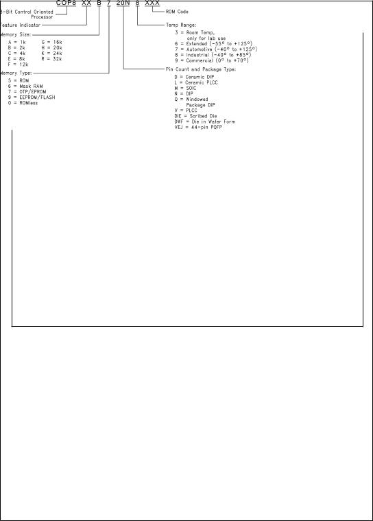
2.1 Ordering Information
DS100973-8
FIGURE 3. Part Numbering Scheme
www.national.com |
4 |

3.0 Electrical Characteristics
Absolute Maximum Ratings (Note 1)
If Military/Aerospace specified devices are required, please contact the National Semiconductor Sales Office/ Distributors for availability and specifications.
Supply Voltage (VCC) |
7V |
Voltage at Any Pin |
−0.3V to V CC +0.3V |
Total Current into VCC |
80 mA |
Pin (Source) |
|
Total Current out of |
|
GND Pin (Sink) |
100 mA |
Storage Temperature |
|
Range |
−65ÊC to +150ÊC |
ESD Protection Level |
2 kV(Human Body Model) |
ESD Protection Level |
|
(CKI pin) |
150 V(Machine Model) |
Note 1: Absolute maximum ratings indicate limits beyond which damage to the device may occur. DC and AC electrical specifications are not ensured when operating the device at absolute maximum ratings.
Note 2: The COP8SER7 is for Engineering Development purpose only and is not recommended for production or pre-production use.
DC Electrical Characteristics
−40ÊC ≤ TA ≤ +85ÊC unless otherwise specified.
|
|
Parameter |
Conditions |
Min |
Typ |
Max |
Units |
|
|
|
|
|
|
|
|
|
Operating Voltage |
|
2.7 |
|
5.5 |
V |
|
|
Power Supply Rise Time |
|
10 |
|
50 x 106 |
ns |
|
Power Supply Ripple (Note 4) |
Peak-to-Peak |
|
|
0.1 Vcc |
V |
||
Supply Current (Note 5) |
VCC = 5.5V, tC = 1 µs |
|
|
|
|
||
|
CKI = 10 MHz |
(SEC5) |
|
|
6 |
mA |
|
|
|
|
(SER7)(Note 13) |
|
|
10 |
mA |
|
|
|
|
|
|
|
|
HALT Current (Note 6) |
VCC = 5.5V, CKI = 0 MHz |
|
|
|
|
||
|
|
|
(SEC5) |
|
8 |
20 |
µA |
|
|
|
(SER7) |
|
|
22 |
µA |
|
|
|
|
|
|
|
|
IDLE Current (Note 5) |
VCC = 5.5V, tC = 1 µs |
|
|
|
|
||
|
CKI = 10 MHz |
(SEC5) |
|
|
1.5 |
mA |
|
|
|
|
(SER7) |
|
|
1.5 |
mA |
|
|
|
|
|
|
|
|
Input Levels (VIH, VIL) |
|
|
|
|
|
||
|
|
|
|
|
|
|
|
|
RESET |
|
|
|
|
|
|
|
Logic High |
|
0.8 Vcc |
|
|
V |
|
|
Logic Low |
|
|
|
0.2 Vcc |
V |
|
CKI, All Other Inputs |
|
|
|
|
|
||
|
Logic High |
|
0.7 Vcc |
|
|
V |
|
|
Logic Low |
|
|
|
0.2 Vcc |
V |
|
Hi-Z Input Leakage |
VCC = 5.5V |
−2 |
|
+2 |
µA |
||
Input Pullup Current |
VCC = 5.5V, VIN = 0V |
−40 |
|
−250 |
µA |
||
G and L Port Input Hysteresis |
VCC = 5.5V |
0.25 Vcc |
|
|
V |
||
|
|
|
VCC = 2.7V |
0.31 Vcc |
|
|
V |
5 |
www.national.com |

DC Electrical Characteristics (Continued)
−40ÊC £ TA £ +85ÊC unless otherwise specified.
Parameter |
Conditions |
Min |
Typ |
Max |
Units |
Output Current Levels |
|
|
|
|
|
Source (Weak Pull-Up Mode) |
VCC = 4.5V, VOH = 2.7V |
−10 |
|
−110 |
µA |
|
VCC = 2.7V, VOH = 1.8V |
−2.5 |
|
−33 |
µA |
Source (Push-Pull Mode) |
VCC = 4.5V, VOH = 3.3V |
−0.4 |
|
|
mA |
|
VCC = 2.7V, VOH = 1.8V |
−0.2 |
|
|
mA |
Sink (Push-Pull Mode) |
VCC = 4.5V, VOL = 0.4V |
1.6 |
|
|
mA |
|
VCC = 2.7V, VOL = 0.4V |
0.7 |
|
|
mA |
TRI-STATE Leakage |
VCC = 5.5V |
−2 |
|
+2 |
µA |
Allowable Sink Current per Pin |
(Note 9) |
|
|
3 |
mA |
|
|
|
|
|
|
Maximum Input Current without Latchup |
Room Temp. |
|
|
±200 |
mA |
(Note 7) |
|
|
|
|
|
|
|
|
|
|
|
RAM Retention Voltage, Vr |
(Note 9) |
2 |
|
|
V |
VCC Rise Time from a VCC ³ 2.0V |
|
6 |
|
|
µs |
Input Capacitance |
(Note 9) |
|
|
7 |
pF |
|
|
|
|
|
|
EERAM Number of Write Cycles |
(Note 9) |
|
105 |
|
cycles |
EERAM Data Retention |
(Note 9) |
10 |
|
|
years |
|
|
|
|
|
|
www.national.com |
6 |

AC Electrical Characteristics
−40ÊC ≤ TA ≤ +85ÊC unless otherwise specified.
Parameter |
|
Conditions |
Min |
Typ |
Max |
Units |
|
|
|
|
|
|
|
Instruction Cycle Time (tC) |
|
|
|
|
|
|
Crystal/Resonator |
4.5V |
≤ VCC ≤ 5.5V |
1 |
|
DC |
µs |
|
2.7V |
≤ VCC < 4.5V |
2 |
|
DC |
µs |
R/C Oscillator |
4.5V |
≤ VCC ≤ 5.5V |
3 |
|
DC |
µs |
|
2.7V |
≤ VCC < 4.5V |
6 |
|
DC |
µs |
Frequency Variation (Note 9), (Note 10) |
4.5V |
≤ VCC ≤ 5.5V |
|
|
±15 |
% |
CKI Clock Duty Cycle (Note 9) |
fr = Max |
45 |
|
55 |
% |
|
Rise Time (Note 9) |
fr = 10 MHz Ext Clock |
|
|
12 |
ns |
|
Fall Time (Note 9) |
fr = 10 MHz Ext Clock |
|
|
8 |
ns |
|
|
|
|
|
|
|
|
EERAM Write Cycle |
|
|
|
7 |
15 |
ms |
|
|
|
|
|
|
|
Delay from Power-Up to first EERAM Write |
|
|
|
|
65 |
µs |
Cycle |
|
|
|
|
|
|
|
|
|
|
|
|
|
Output Propagation Delay (Note 8) |
|
|
|
|
|
|
tPD1, tPD0 |
RL = 2.2k, CL = 100 |
|
|
|
|
|
|
pF |
|
|
|
|
|
SO, SK |
4.5V |
≤ VCC ≤ 5.5V |
|
|
0.7 |
µs |
|
2.7V |
≤ VCC < 4.5V |
|
|
1.75 |
µs |
All Others |
4.5V |
≤ VCC ≤ 5.5V |
|
|
1 |
µs |
|
2.7V |
≤ VCC < 4.5V |
|
|
2.5 |
µs |
MICROWIRE Setup Time (tUWS) (Note 12) |
|
|
20 |
|
|
ns |
MICROWIRE Hold Time (tUWH) (Note 12) |
|
|
56 |
|
|
ns |
MICROWIRE Output Propagation Delay |
|
|
|
|
220 |
ns |
(tUPD)(Note 12) |
|
|
|
|
|
|
Input Pulse Width (Note 9) |
|
|
|
|
|
|
Interrupt Input High Time |
|
|
1 |
|
|
tC |
Interrupt Input Low Time |
|
|
1 |
|
|
tC |
Timer 1 Input High Time |
|
|
1 |
|
|
tC |
Timer 1 Input Low Time |
|
|
1 |
|
|
tC |
Reset Pulse Width |
|
|
1 |
|
|
µs |
Note 3: tC = Instruction cycle time.
Note 4: Maximum rate of voltage change must be < 0.5 V/ms.
Note 5: Supply and IDLE currents are measured with CKI driven with a square wave Oscillator, CKO driven 180Ê out of phase with CKI, inputs connected to VCC and outputs driven low but not connected to a load.
Note 6: The HALT mode will stop CKI from oscillating in the R/C and the Crystal configurations. In the R/C configuration, CKI is forced high internally. In the crystal configuration, CKI is TRI-STATE. Measurement of IDD HALT is done with device neither sourcing nor sinking current; with L, G0, and G2±G5 programmed as low outputs and not driving a load; all outputs programmed low and not driving a load; all inputs tied to VCC; WATCHDOG and clock monitor disabled. Parameter refers to HALT mode entered via setting bit 7 of the G Port data register.
Note 7: Pins G6 and RESET are designed with a high voltage input network. These pins allow input voltages > VCC and the pins will have sink current to VCC when biased at voltages > VCC (the pins do not have source current when biased at a voltage below VCC). The effective resistance to VCC is 750Ω (typical). These two pins will not latch up. The voltage at the pins must be limited to < 14V. WARNING: Voltages in excess of 14V will cause damage to the pins. This warning excludes ESD transients.
Note 8: The output propagation delay is referenced to the end of the instruction cycle where the output change occurs.
Note 9: Parameter characterized but not tested.
Note 10: Rise times faster than the minimum specification may trigger an internal power-on-reset.
Note 11: Exclusive of R and C variation.
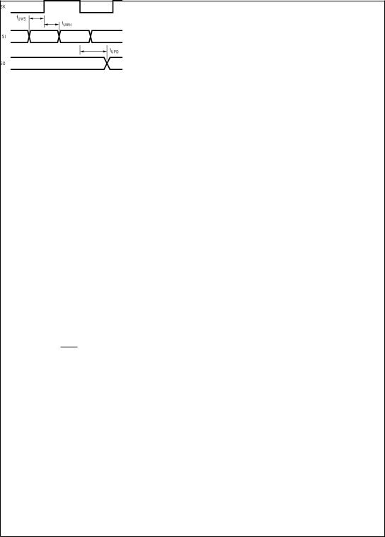
Note 12: MICROWIRE Setup and Hold Times and Propagation Delays are referenced to the appropriate edge of the MICROWIRE clock. See Figure 4 and the MICROWIRE operation description.
Note 13: COP7SER7 Supply Current during Reset will be somewhat higher.
7 |
www.national.com |

Absolute Maximum Ratings (Note 14)
If Military/Aerospace specified devices are required, please contact the National Semiconductor Sales Office/ Distributors for availability and specifications.
Supply Voltage (VCC) |
7V |
Voltage at Any Pin |
−0.3V to V CC +0.3V |
Total Current into VCC Pin |
80 mA |
(Source) |
|
Total Current out of GND Pin |
|
(Sink) |
100 mA |
Storage Temperature Range |
−65ÊC to +150ÊC |
ESD Protection Level |
2kV (Human Body |
|
Model) |
ESD Protection Level (CKI |
150 V (Machine |
pin) |
Model) |
Note 14: Absolute maximum ratings indicate limits beyond which damage to the device may occur. DC and AC electrical specifications are not ensured when operating the device at absolute maximum ratings.
Note 15: The COP8SER7 is for Engineering Development purpose only and is not recommended for production or pre-production use.
DC Electrical Characteristics (SEC5 only)
−40ÊC £ TA £ +135ÊC unless otherwise specified.
|
|
Parameter |
Conditions |
Min |
Typ |
Max |
Units |
|
|
|
|
|
|
|
|
|
Operating Voltage |
|
4.5 |
|
5.5 |
V |
|
|
Power Supply Rise Time |
|
10 |
|
50 x 106 |
ns |
|
Power Supply Ripple (Note 17) |
Peak-to-Peak |
|
|
0.1 Vcc |
V |
||
Supply Current (Note 18) |
|
|
|
|
|
||
|
CKI = 10 MHz |
VCC = 5.5V, tC = 1 µs |
|
|
8 |
mA |
|
HALT Current (Note 19) |
VCC = 5.5V, CKI = 0 MHz |
|
15 |
50 |
µA |
||
IDLE Current (Note 18) |
|
|
|
|
|
||
|
CKI = 10 MHz |
VCC = 5.5V, tC = 1 µs |
|
|
2 |
mA |
|
Input Levels (VIH, VIL) |
|
|
|
|
|
||
|
|
|
|
|
|
|
|
|
RESET |
|
|
|
|
|
|
|
Logic High |
|
0.8 Vcc |
|
|
V |
|
|
Logic Low |
|
|
|
0.2 Vcc |
V |
|
CKI, All Other Inputs |
|
|
|
|
|
||
|
Logic High |
|
0.7 Vcc |
|
|
V |
|
|
Logic Low |
|
|
|
0.2 Vcc |
V |
|
Hi-Z Input Leakage |
VCC = 5.5V |
−5 |
|
+5 |
µA |
||
Input Pullup Current |
VCC = 5.5V, VIN = 0V |
−35 |
|
−400 |
µA |
||
G and L Port Input Hysteresis |
VCC = 5.5V |
0.25 |
|
|
V |
||
|
|
|
|
Vcc |
|
|
|
Output Current Levels |
|
|
|
|
|
||
|
Source (Weak Pull-Up Mode) |
VCC = 4.5V, VOH = 2.7V |
−9.0 |
|
−140 |
µA |
|
|
Source (Push-Pull Mode) |
VCC = 4.5V, VOH = 3.3V |
−0.4 |
|
|
mA |
|
|
Sink (Push-Pull Mode) |
VCC = 4.5V, VOL = 0.4V |
1.6 |
|
|
mA |
|
TRI-STATE Leakage |
VCC = 5.5V |
−5 |
|
+5 |
µA |
||
Allowable Sink Current per Pin (Note 22) |
|
|
|
|
|
||
|
|
|
|
|
|
|
|
Maximum Input Current without Latchup (Note |
Room Temp. |
|
|
±200 |
mA |
||
20) |
|
|
|
|
|||
|
|
|
|
|
|
||
|
|
|
|
|
|
|
|
RAM Retention Voltage, Vr |
|
2.0 |
|
|
V |
||
VCC Rise Time from a VCC ³ 2.0V |
(Note 23) |
6 |
|
|
µs |
||
Input Capacitance |
(Note 22) |
|
|
7 |
pF |
||
|
|
|
|
|
|
|
|
EERAM Number of Write Cycles |
(Note 22) |
|
105 |
|
cycles |
||
EERAM Data Retention |
(Note 22) |
10 |
|
|
years |
||
www.national.com |
8 |
AC Electrical Characteristics
−40ÊC ≤ TA ≤ +135ÊC unless otherwise specified.
Parameter |
Conditions |
Min |
Typ |
Max |
Units |
|
|
|
|
|
|
Instruction Cycle Time (tC) |
|
|
|
|
|
Crystal/Resonator, External |
4.5V ≤ VCC ≤ 5.5V |
1 |
|
DC |
µs |
R/C Oscillator (Internal) |
4.5V ≤ VCC ≤ 5.5V |
3 |
|
DC |
µs |
Frequency Variation (Note 22), (Note 21) |
4.5V ≤ VCC ≤ 5.5V |
|
|
±20 |
% |
CKI Clock Duty Cycle (Note 22) |
fr = Max |
45 |
|
55 |
% |
Rise Time (Note 22) |
fr = 10 MHz Ext Clock |
|
|
12 |
ns |
Fall Time (Note 22) |
fr = 10 MHz Ext Clock |
|
|
8 |
ns |
|
|
|
|
|
|
EERAM Write Cycle |
|
|
7 |
15 |
ms |
|
|
|
|
|
|
Delay from Power-up to first EERAM Write |
|
|
|
65 |
µs |
Cycle |
|
|
|
|
|
|
|
|
|
|
|
Output Propagation Delay (Note 21) |
RL = 2.2k, CL = 100 |
|
|
|
|
|
pF |
|
|
|
|
tPD1, tPD0 |
|
|
|
|
|
SO, SK |
4.5V ≤ VCC ≤ 5.5V |
|
|
0.7 |
µs |
All Others |
4.5V ≤ VCC ≤ 5.5V |
|
|
1.0 |
µs |
MICROWIRE Setup Time (tUWS) (Note 25) |
|
20 |
|
|
ns |
MICROWIRE Hold Time (tUWH) (Note 25) |
|
56 |
|
|
ns |
MICROWIRE Output Propagation Delay |
|
|
|
220 |
ns |
(tUPD) (Note 25) |
|
|
|
|
|
Input Pulse Width (Note 22) |
|
|
|
|
|
Interrupt Input High Time |
|
1 |
|
|
tC |
Interrupt Input Low Time |
|
1 |
|
|
tC |
Timer 1 Input High Time |
|
1 |
|
|
tC |
Timer 1 Input Low Time |
|
1 |
|
|
tC |
Reset Pulse Width |
|
1 |
|
|
µs |
|
|
|
|
|
|
Note 16: tC = Instruction cycle time.
Note 17: Maximum rate of voltage change must be < 0.5 V/ms.
Note 18: Supply and IDLE currents are measured with CKI driven with a square wave Oscillator, CKO driven 180Ê out of phase with CKI, inputs connected to VCC and outputs driven low but not connected to a load.
Note 19: The HALT mode will stop CKI from oscillating in the R/C and the Crystal configurations. In the R/C configuration, CKI is forced high internally. In the crystal configuration, CKI is TRI-STATE. Measurement of IDD HALT is done with device neither sourcing nor sinking current; with L, G0, and G2±G5 programmed as low outputs and not driving a load; all outputs programmed low and not driving a load; all inputs tied to VCC; clock monitor disabled. Parameter refers to HALT mode entered via setting bit 7 of the G Port data register.
Note 20: Pins G6 and RESET are designed with a high voltage input network. These pins allow input voltages > VCC and the pins will have sink current to VCC when biased at voltages > VCC (the pins do not have source current when biased at a voltage below VCC). The effective resistance to VCC is 750Ω (typical). These two pins will not latch up. The voltage at the pins must be limited to < 14V. WARNING: Voltages in excess of 14V will cause damage to the pins. This warning excludes ESD transients.
Note 21: The output propagation delay is referenced to the end of the instruction cycle where the output change occurs.
Note 22: Parameter characterized but not tested.
Note 23: Rise times faster than the minimum specification may trigger an internal power-on-reset.
Note 24: Exclusive of R and C variation.
Note 25: MICROWIRE Setup and Hold Times and Propagation Delays are referenced to the appropriate edge of the MICROWIRE clock. See Figure 4 and the MICROWIRE operation description.
DS100973-9
FIGURE 4. MICROWIRE/PLUS Timing
9 |
www.national.com |
4.0 Pin Descriptions
The device I/O structure enables designers to reconfigure the microcontroller's I/O functions with a single instruction. Each individual I/O pin can be independently configured as output pin low, output high, input with high impedance or input with weak pull-up device. A typical example is the use of I/O pins as the keyboard matrix input lines. The input lines can be programmed with internal weak pull-ups so that the input lines read logic high when the keys are all open. With a key closure, the corresponding input line will read a logic zero since the weak pull-up can easily be overdriven. When the key is released, the internal weak pull-up will pull the input line back to logic high. This eliminates the need for external pull-up resistors. The high current options are available for driving LEDs, motors and speakers. This flexibility helps to ensure a cleaner design, with fewer external components and lower costs. Below is the general description of all available pins.
VCC and GND are the power supply pins. All VCC and GND pins must be connected.
CKI is the clock input. This can come from the Internal R/C oscillator, or a crystal oscillator (in conjunction with CKO). See Oscillator Description section.
RESET is the master reset input. See Reset description section.
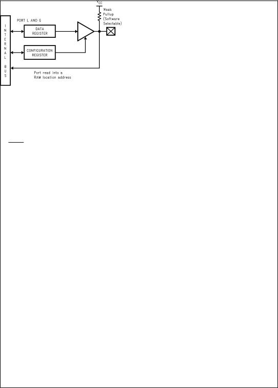
Each device contains two bidirectional 8-bit I/O ports (G and L) and one bidirectional 4-I/O port (F), where each individual bit may be independently configured as an input (Schmitt trigger inputs on ports L and G), output or TRI-STATE under program control. Three data memory address locations are allocated for each of these I/O ports. Each I/O port has two associated 8-bit memory mapped registers, the CONFIGURATION register and the output DATA register. A memory mapped address is also reserved for the input pins of each I/O port. (See the memory map for the various addresses associated with the I/O ports.) Figure 5 shows the I/O port configurations. The DATA and CONFIGURATION registers allow for each port bit to be individually configured under software control as shown below:
CONFIGURATION |
DATA |
Port Set-Up |
|
Register |
Register |
||
|
|||
|
|
|
|
0 |
0 |
Hi-Z Input |
|
|
|
(TRI-STATE Output) |
|
|
|
|
|
0 |
1 |
Input with Weak Pull-Up |
|
|
|
|
|
1 |
0 |
Push-Pull Zero Output |
|
|
|
|
|
1 |
1 |
Push-Pull One Output |
|
|
|
|
Port L is an 8-bit I/O port. All L-pins have Schmitt triggers on the inputs.
Port L supports the Multi-Input Wake Up feature on all eight pins.
Port G is an 8-bit port. Pin G0, G2±G5 are bi-directional I/O ports. Pin G6 is always a general purpose Hi-Z input. All pins have Schmitt Triggers on their inputs. Pin G1 serves as the dedicated WATCHDOG output with weak pullup, if WATCHDOG feature is selected by the mask option. The pin is a general purpose I/O, if WATCHDOG feature is not selected. If WATCHDOG feature is selected, bit 1 of the Port G configuration and data register does not have any effect on Pin G1 setup. Pin G7 is either input or output depending on the oscillator option selected. With the crystal oscillator option selected, G7 serves as the dedicated output pin for the CKO clock output. With the R/C oscillator option selected, G7 serves as a general purpose Hi-Z input pin and is also used to bring the device out of HALT mode with a low to high transition on G7.
Since G6 is an input only pin and G7 is the dedicated CKO clock output pin (crystal clock option) or general purpose input (R/C or clock option), the associated bits in the data and configuration registers for G6 and G7 are used for special purpose functions as outlined below. Reading the G6 and G7 data bits will return zeroes.
Each device will be placed in the HALT mode by writing a ª1º to bit 7 of the Port G Data Register. Similarly the device will be placed in the IDLE mode by writing a ª1º to bit 6 of the Port G Data Register.
Writing a ª1º to bit 6 of the Port G Configuration Register enables the MICROWIRE/PLUS to operate with the alternate phase of the SK clock. The G7 configuration bit, if set high, enables the clock start up delay after HALT when the R/C clock configuration is used.
|
Config. Reg. |
Data Reg. |
|
|
|
G7 |
CLKDLY |
HALT |
|
|
|
G6 |
Alternate SK |
IDLE |
|
|
|
Port G has the following alternate features:
G7 CKO Oscillator dedicated output or general purpose input
G6 SI (MICROWIRE Serial Data Input)
G5 SK (MICROWIRE Serial Clock)
G4 SO (MICROWIRE Serial Data Output)
G3 T1A (Timer T1 I/O)
G2 T1B (Timer T1 Capture Input)
G1 WDOUT WATCHDOG and/or CLock Monitor if WATCHDOG enabled, otherwise it is a general purpose I/O (General purpose I/O is not available on COP8SER7)
G0 INTR (External Interrupt Input)
DS100973-10
FIGURE 5. I/O Port Configurations
www.national.com |
10 |
4.0 Pin Descriptions (Continued)
DS100973-12
FIGURE 6. I/O Port Configurations Ð Output Mode
DS100973-11
FIGURE 7. I/O Port Configurations Ð Input Mode
5.0 Functional Description
The architecture of the devices is a modified Harvard architecture. With the Harvard architecture, the program memory ROM or EPROM is separated from the data store memory (RAM). Program Memory will be referred to as ROM. Both ROM and RAM have their own separate addressing space with separate address buses. The architecture, though based on the Harvard architecture, permits transfer of data from ROM to RAM.
5.1 CPU REGISTERS
The CPU can do an 8-bit addition, subtraction, logical or shift operation in one instruction (tC) cycle time.
There are six CPU registers:
A is the 8-bit Accumulator Register
PC is the 15-bit Program Counter Register
PU is the upper 7 bits of the program counter (PC)
PL is the lower 8 bits of the program counter (PC)
B is an 8-bit RAM address pointer, which can be optionally post auto incremented or decremented.
X is an 8-bit alternate RAM address pointer, which can be optionally post auto incremented or decremented.
S is the 8-bit Segment Address Register used to extend the lower half of the address range (00 to 7F) into 256 data segments of 128 bytes each.
SP is the 8-bit stack pointer, which points to the subroutine/ interrupt stack (in RAM). With reset the SP is initialized to RAM address 02F Hex (devices with 64 bytes of RAM), or initialized to RAM address 06F Hex (devices with 128 bytes of RAM).
All the CPU registers are memory mapped with the exception of the Accumulator (A) and the Program Counter (PC).
5.2 PROGRAM MEMORY
The program memory consists of 4096 Bytes of ROM or 32,768 bytes of OTP EPROM. These bytes may hold program instructions or constant data (data tables for the LAID instruction, jump vectors for the JID instruction, and interrupt vectors for the VIS instruction). The program memory is addressed by the 15-bit program counter (PC). All interrupts in the device vector to program memory location 0FF Hex. The contents of the program memory read 00 Hex in the erased state. Program execution starts at location 0 after RESET.
5.3 DATA MEMORY
The data memory address space includes the on-chip RAM and data registers, the I/O registers (Configuration, Data and Pin), the control registers, the MICROWIRE/PLUS SIO shift register, and the various registers, and counters associated with the timers (with the exception of the IDLE timer). Data memory is addressed directly by the instruction or indirectly by the B, X and SP pointers.
The data memory consists of 256 bytes of combined EERAM and RAM. Sixteen bytes of RAM are mapped as ªregistersº at addresses 0F0 to 0FE Hex. These registers can be loaded immediately, and also decremented and tested with the DRSZ (decrement register and skip if zero) instruction. The memory pointer registers X, SP and B are memory mapped into this space at address locations 0FC to 0FE Hex respectively, with the other registers (except 0FF) being available for general usage.
The instruction set permits any bit in memory to be set, reset or tested. All I/O and registers (except A and PC) are memory mapped; therefore, I/O bits and register bits can be directly and individually set, reset and tested. The accumulator (A) bits can also be directly and individually tested.
Note: RAM contents are undefined upon power-up.
5.4 EERAM / NON-VOLATILE MEMORY
The devices provide 128 bytes of EERAM in segment 1 for nonvolatile data memory. The data EERAM can be read and written in exactly the same way as the RAM. All instructions that perform read and write operations on the RAM work similarly upon the data EERAM. EERAM write cycles take much more time than reads. During this time, processing continues, but all EERAM accesses are inhibited. The data EERAM contains all 00s when shipped by the factory.
A data memory EERAM programming cycle is initiated by an instruction that writes to the EERAM such as X, LD, SBIT and RBIT. The EERAM memory support circuitry sets the E2BUSY flag in the E2CFG register immediately upon beginning a data EERAM write cycle. It will be automatically reset by the hardware at the end of the data EERAM write cycle. The application program should test the E2BUSY flag before attempting a read or write operation to the data EERAM. An EERAM read or write operation while an operation is in progress will be ignored and the E2ILRW flag in the E2CFG register will be set to indicate the error status. Once the write operation starts, nothing will stop the write operation, not by resetting the device, and not even turning off the VCC will guarantee the write operation to stop.
11 |
www.national.com |
5.0 Functional Description (Continued)
Caution: In order to prevent the unexpected setting of the ILRW of the E2CFG Register and the corresponding interrupt, the use of the X Register and direct addressing are recommanded for EERAM access. It is further recommended that the B Register be set to a value between 80 (hex) and FF (hex) before setting the Segment register to 1 and that this value be retained until S is set back to 0.
Due to an artifact of the COP8 architecture, the ILRW bit of the E2CFG Register will be set and an interrupt will be generated under the following conditions:
1.The Segment Register (S) = 01, and
2.The B Register points to the EERAM, i.e. B ≤7F (hex), and
3.One of the following instructions is executed: SC, RC, IFC, IFNC, NOP, RPND, SWAPA, JMPL, VIS or LD B, Imm with Imm ≤7F (hex),
or
3a. if any instruction is skipped.
Warning: The segment register should not point to the EERAM unless the EERAM is addressed. This will prevent inadvertent writes to EERAM.
5.4.1. E2CFG and EE Support Circuitry
The EERAM module contains EERAM support circuits to generate all necessary high voltage programming pulses. The E2CFG register provides control and status functions for the EERAM module. The E2CFG register bit assignments are shown below. The E2CFG register is set to 0 on RESET except the E2BUSY bit, which is unaffected. The EECFG register can be accessed at any time without error.
Reserved, must be 0 |
E2PEND |
E2ILRW |
E2BUSY |
E2EI |
|||
|
|
|
|
|
|
|
|
R/W |
R/W |
R/W |
R/W |
R/W |
R/W |
RO |
R/W |
|
|
|
|
|
|
|
|
Bit 7 |
|
|
|
Bit 0 |
|||
|
|
|
|
|
|
|
|
RESERVED These bits are reserved and must be 0.
E2PEND |
Interrupt Pending Bit. This bit indicates that |
|
a write operation has completed and a Write |
|
Complete Interrupt is pending. This bit is |
|
logically ANDed with the E2EI bit to cause |
|
an interrupt. This bit can be written by either |
|
hardware or software. This bit must be reset |
|
by software after processing the interrupt. |
E2ILRW |
EERAM illegal read/write operation. This bit |
|
is set when the EERAM array is accessed |
|
while E2BUSY is set. This bit will cause an |
|
EERAM interrupt, without setting the |
|
E2PEND bit, if the E2EI bit is set. This bit |
|
can be written by either hardware or soft- |
|
ware. This bit must be reset by software af- |
|
ter processing the interrupt. |
E2BUSY |
This bit is set by the hardware when a write |
|
to the EERAM is in process and reset by the |
|
hardware when the write completes. The |
|
E2PEND bit is set when this bit is reset. |
|
This bit is software read-only. |
E2EI |
Interrupt Enable Bit. Setting this bit enables |
|
EERAM interrupts. The default condition is |
|
interrupts disabled after RESET. This bit |
|
must be used in conjunction with the GIE |
|
bit. This bit can be written by software only. |
5.5 DATA MEMORY SEGMENT RAM EXTENSION
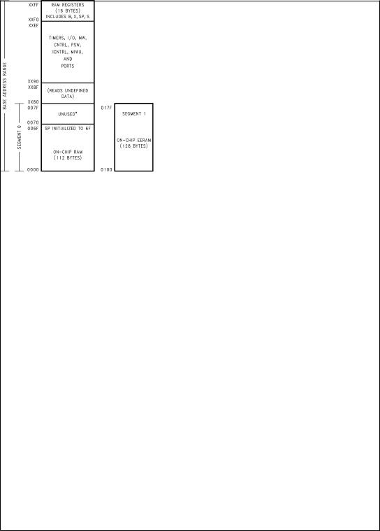
Data memory address 0FF is used as a memory mapped location for the Data Segment Address Register (S).
The data store memory is either addressed directly by a single byte address within the instruction, or indirectly relative to the reference of the B, X, or SP pointers (each contains a single-byte address). This single-byte address allows an addressing range of 256 locations from 00 to FF hex. The upper bit of this single-byte address divides the data store memory into two separate sections as outlined previously. With the exception of the RAM register memory from address locations 00F0 to 00FF, all RAM memory is memory mapped with the upper bit of the single-byte address being equal to zero. This allows the upper bit of the single-byte address to determine whether or not the base address range (from 0000 to 00FF) is extended. If this upper bit equals one (representing address range 0080 to 00FF), then address extension does not take place. Alternatively, if this upper bit equals zero, then the data segment extension register S is used to extend the base address range (from 0000 to 007F) from XX00 to XX7F, where XX represents the 8 bits from the S register. Thus the 128-byte data segment extensions are located from addresses 0100 to 017F for data segment 1, 0200 to 027F for data segment 2, etc., up to FF00 to FF7F for data segment 255. The base address range from 0000 to 007F represents data segment 0.
Figure 8 illustrates how the S register data memory extension is used in extending the lower half of the base address range (00 to 7F hex) into 256 data segments of 128 bytes each, with a total addressing range of 32 kbytes from XX00 to XX7F. This organization allows a total of 256 data segments of 128 bytes each with an additional upper base segment of 128 bytes. Furthermore, all addressing modes are available for all data segments. The S register must be changed under program control to move from one data segment (128 bytes) to another. However, the upper base segment (containing the 16 memory registers, I/O registers, control registers, etc.) is always available regardless of the contents of the S register, since the upper base segment (address range 0080 to 00FF) is independent of data segment extension.
DS100973-45
FIGURE 8. RAM Organization
The instructions that utilize the stack pointer (SP) always reference the stack as part of the base segment (Segment 0), regardless of the contents of the S register. The S register is
www.national.com |
12 |

5.0 Functional Description (Continued)
not changed by these instructions. Consequently, the stack (used with subroutine linkage and interrupts) is always located in the base segment. The stack pointer will be initialized to point at data memory location 006F as a result of reset.
The 128 bytes of RAM contained in the base segment are split between the lower and upper base segments. The first 112 bytes of RAM are resident from address 0000 to 006F in the lower base segment, while the remaining 16 bytes of RAM represent the 16 data memory registers located at addresses 00F0 to 00FF of the upper base segment. No RAM is located at the upper sixteen addresses (0070 to 007F) of the lower base segment.
Additional RAM beyond these initial 128 bytes, however, will always be memory mapped in groups of 128 bytes (or less) at the data segment address extensions (XX00 to XX7F) of the lower base segment. The 128 bytes of EERAM in this device are memory mapped at address locations 0100 to 017F.
5.6 SECURITY FEATURE (COP8SER7 only)
The program memory array has an associated Security Byte that is located outside of the program address range. This byte can be addressed only from programming mode by a programmer tool.
Security is an optional feature and can only be asserted after the memory array has been programmed and verified. A secured part will read 00(hex) by a programmer. The part will fail Blank Check and will fail Verify operations. A READ operation will fill the programmer's memory with 00(hex). The Security Byte itself is always readable with value of 00(hex) if unsecure and FF(hex) if secure.
5.7 RESET
The devices are initialized when the RESET pin is pulled low.
The following occurs upon initialization:
Port L: TRI-STATE (High Impedance Input)
Port G: TRI-STATE (High Impedance Input)
PC: CLEARED to 0000
PSW, CNTRL and ICNTRL registers: CLEARED
SIOR:
UNAFFECTED after RESET with power already applied
RANDOM after RESET at power-on
Accumulator, Timer 1:
RANDOM after RESET with crystal clock option
(power already applied)
UNAFFECTED after RESET with R/C clock option
(power already applied)
RANDOM after RESET at power-on
WKEN, WKEDG: CLEARED
WKPND: RANDOM
SP (Stack Pointer):
Initialized to RAM address 06F Hex
B and X Pointers:
UNAFFECTED after RESET with power already applied
RANDOM after RESET at power-on
S Register: CLEARED
E2CFG: Cleared except the E2BUSY Bit (Bit 1)
EERAM: Unaffected
ITMR: Cleared
RAM:
UNAFFECTED after RESET with power already applied
RANDOM after RESET at power-on
WATCHDOG (if enabled):
The device comes out of reset with both the WATCHDOG logic and the Clock Monitor detector armed, with the WATCHDOG service window bits set and the Clock Monitor bit set. The WATCHDOG and Clock Monitor circuits are inhibited during reset. The WATCHDOG service window bits being initialized high default to the maximum WATCHDOG service window of 64k tC clock cycles. The Clock Monitor bit being initialized high will cause a Clock Monitor error following reset if the clock has not reached the minimum specified frequency at the termination of reset. A Clock Monitor error will cause an active low error output on pin G1. This error output will continue until 16 tC±32 tC clock cycles following the clock frequency reaching the minimum specified value, at which time the G1 output will go high.
5.8.1 External Reset
The RESET input when pulled low initializes the device. The RESET pin must be held low for a minimum of one instruction cycle to guarantee a valid reset. During Power-Up initialization, the user must ensure that the RESET pin is held low until the device is within the specified VCC voltage. An R/C circuit on the RESET pin with a delay 5 times (5x) greater than the power supply rise time is recommended. Reset should also be wide enough to ensure crystal start-up upon Power-Up.
RESET may also be used to cause an exit from the HALT mode.
A recommended reset circuit for this device is shown in Figure 9.
DS100973-14
RC >5x power supply rise time.
FIGURE 9. Reset Circuit Using External Reset
5.9 OSCILLATOR CIRCUITS
These devices can be driven by a clock input on the CKI input pin which can be between DC and 10 MHz. The CKO output clock is on pin G7 (crystal configuration). The CKI input frequency is divided down by 10 to produce the instruction cycle clock (1/tC ).
Figure 10 shows the crystal and R/C oscillator connection diagram.
13 |
www.national.com |
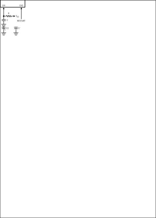
5.0 Functional Description (Continued)
DS100973-51
DS100973-50
FIGURE 10. Crystal and R/C Oscillator
5.9.1 Crystal Oscillator
CKI and CKO can be connected to make a closed loop crystal (or resonator) controlled oscillator.
Table 1 shows the component values required for various standard crystal values.
5.9.2 R/C Oscillator
By selecting CKI as a single pin oscillator input, a single pin R/C oscillator circuit can be connected to it. CKO is available as a general purpose input, and /or HALT restart input.
Table 2 shows the variation in the oscillator frequency as a function of the component (R and C) value.
TABLE 1. Crystal Oscillator Configuration,
TA = 25ÊC, VCC = 5V
R1 (kΩ) |
R2 (MΩ) |
C1 (pF) |
C2 (pF) |
CKI Freq. |
|
(MHz) |
|||||
|
|
|
|
||
|
|
|
|
|
|
0 |
1 |
32 |
32 |
10 |
|
|
|
|
|
|
|
0 |
1 |
39 |
39 |
4 |
|
|
|
|
|
|
|
5.6 |
1 |
100 |
100±156 |
0.455 |
|
|
|
|
|
|
TABLE 2. R/C Oscillator Configuration,
TA = 25ÊC, VCC = 5V
R (kΩ) |
C (pF) |
CKI Freq.(MHz) |
Instr. Cycle (µs) |
|
|
|
|
3.3 |
82 |
2.2 to 2.7 |
3.7 to 4.6 |
|
|
|
|
5.6 |
100 |
1.1 to 1.3 |
7.4 to 9.0 |
|
|
|
|
6.8 |
100 |
0.9 to 1.1 |
8.8 to 10.8 |
|
|
|
|
www.national.com |
14 |

5.0Functional Description (Continued)
5.10CONTROL REGISTERS
CNTRL Register (Address X©00EE)
T1C3 |
T1C2 |
T1C1 |
T1C0 |
MSEL |
IEDG |
SL1 |
SL0 |
|
|
|
|
|
|
|
|
Bit 7 |
Bit 0 |
||||||
|
|
|
|
|
|
|
|
The Timer1 (T1) and MICROWIRE/PLUS control register contains the following bits:
T1C3 |
Timer T1 mode control bit |
T1C2 |
Timer T1 mode control bit |
T1C1 |
Timer T1 mode control bit |
T1C0 |
Timer T1 Start/Stop control in timer |
|
modes 1 and 2, T1 Underflow Interrupt |
|
Pending Flag in timer mode 3 |
MSEL |
Selects G5 and G4 as MICROWIRE/PLUS |
|
signals SK and SO respectively |
IEDG |
External interrupt edge polarity select |
|
(0 = Rising edge, 1 = Falling edge) |
SL1 & SL0 |
Select the MICROWIRE/PLUS clock divide |
|
by (00 = 2, 01 = 4, 1x = 8) |
PSW Register (Address X©00EF)
HC |
C |
T1PNDA |
T1ENA |
EXPND |
BUSY |
EXEN |
GIE |
|
|
|
|
|
|
|
|
Bit 7 |
|
|
|
|
|
|
Bit 0 |
|
|
|
|
|
|
|
|
The PSW register contains the following bits:
HC |
Half Carry Flag |
C |
Carry Flag |
T1PNDA Timer T1 Interrupt Pending Flag (Autoreload RA in mode 1, T1 Underflow in Mode 2, T1A capture edge in mode 3)
T1ENA |
Timer T1 Interrupt Enable for Timer Underflow |
|
or T1A Input capture edge |
EXPND |
External interrupt pending |
BUSY |
MICROWIRE/PLUS busy shifting flag |
EXEN |
Enable external interrupt |
GIE |
Global interrupt enable (enables interrupts) |
The Half-Carry flag is also affected by all the instructions that affect the Carry flag. The SC (Set Carry) and R/C (Reset Carry) instructions will respectively set or clear both the carry flags. In addition to the SC and R/C instructions, ADC, SUBC, RRC and RLC instructions affect the Carry and Half Carry flags.
ICNTRL Register (Address X©00E8)
Reserved |
LPEN |
|
T0PND |
T0EN |
µWPND |
µWEN |
T1PNDB |
T1ENB |
|
|
|
|
|
|
|
|
|
Bit 7 |
|
|
|
|
|
|
Bit 0 |
|
|
|
|
|
|
|
|
|
|
The ICNTRL register contains the following bits: |
||||||||
Reserved |
This bit is reserved and must be set to zero |
|||||||
LPEN |
L Port Interrupt Enable (Multi-Input Wakeup/ |
|||||||
|
|
Interrupt) |
||||||
T0PND |
Timer T0 Interrupt pending |
|||||||
T0EN |
Timer T0 Interrupt Enable (Bit 12 toggle) |
|||||||
µWPND |
MICROWIRE/PLUS interrupt pending |
|||||||
µWEN |
Enable MICROWIRE/PLUS interrupt |
|||||||
T1PNDB |
Timer T1 Interrupt Pending Flag for T1B cap- |
|||||||
|
|
ture edge |
||||||
T1ENB |
Timer T1 Interrupt Enable for T1B Input cap- |
|||||||
|
|
ture edge |
||||||
6.0 Timers
Each device contains a very versatile set of timers (T0 and T1). All timers and associated autoreload/capture registers power up containing random data.
6.1 TIMER T0 (IDLE TIMER)
Each device supports applications that require maintaining real time and low power with the IDLE mode. This IDLE mode support is furnished by the IDLE timer T0, which is a 16-bit timer. The Timer T0 runs continuously at the fixed rate of the instruction cycle clock, tC. The user cannot read or write to the IDLE Timer T0, which is a count down timer.
The Timer T0 supports the following functions:
·Exit out of the Idle Mode (See Idle Mode description)
·WATCHDOG logic (See WATCHDOG description)
·Start up delay out of the HALT mode
Figure 11 is a functional block diagram showing the structure of the IDLE Timer and its associated interrupt logic.
Bits 11 through 15 of the Idle Timer register can be selected for triggering the IDLE Timer interrupt. Each time the selected bit underflows (every 4k, 8k, 16k, 32k or 64k instruction cycles), the IDLE Timer interrupt pending bit T0PND is set, thus generating an interrupt (if enabled), and bit 6 of the Port G data register is reset, thus causing an exit from the IDLE mode if the device is in that mode.
In order for an interrupt to be generated, the IDLE Timer interrupt enable bit T0EN must be set, and the GIE (Global Interrupt Enable) bit must also be set. The T0PND flag and T0EN bit are bits 5 and 4 of the ICNTRL register, respectively. The interrupt can be used for any purpose. Typically, it is used to perform a task upon exit from the IDLE mode. For more information on the IDLE mode, refer to the Power Save Modes section.
The Idle Timer period is selected by bits 0±2 of the ITMR register Bits 3±7 of the ITMR Register are reserved and must be ª0º.
TABLE 3. Idle Timer Window Length
ITSEL2 |
ITSEL1 |
ITSEL0 |
Idle Timer Period |
|
|
|
(Instruction Cycles) |
|
|
|
|
0 |
0 |
0 |
4,096 |
|
|
|
|
0 |
0 |
1 |
8,192 |
|
|
|
|
0 |
1 |
0 |
16,384 |
|
|
|
|
0 |
1 |
1 |
32,768 |
|
|
|
|
1 |
X |
X |
65,536 |
|
|
|
|
The ITMR register is cleared on Reset and the Idle Timer period is reset to 4,096 instruction cycles.
ITMR Register (Address X'0xCF)
Reserved (Must be ²0²) |
|
ITSEL2 |
ITSEL1 |
ITSEL0 |
|
|
|
|
|
Bit 7 |
Bit 3 |
|
|
Bit 0 |
|
|
|
|
|
Any time the IDLE Timer period is changed there is the possibility of generating a spurious IDLE Timer interrupt by setting the T0PND bit. The user is advised to disable IDLE Timer interrupts prior to changing the value of the ITSEL bits of the ITMR Register and then clear the T0PND bit before attempting to synchronize operation to the IDLE Timer.
15 |
www.national.com |
 Loading...