


NSC LF13333M, LF13333D, LF13332N, LF13332M, LF13331N Datasheet
...January 1995
LF11331/LF13331/LF11332/LF13332/LF11333/
LF13333/LF11201/LF13201/LF11202/LF13202 Quad SPST JFET Analog Switches
General Description
These devices are a monolithic combination of bipolar and JFET technology producing the industry's first one chip quad JFET switch. A unique circuit technique is employed to maintain a constant resistance over the analog voltage range of
±10V. The input is designed to operate from minimum TTL levels, and switch operation also ensures a break-before-make action.
These devices operate from ±15V supplies and swing a
±10V analog signal. The JFET switches are designed for applications where a dc to medium frequency analog signal needs to be controlled.
Features
nAnalog signals are not loaded
nConstant ªONº resistance for signals up to±10V and 100 kHz
nPin compatible with CMOS switches with the advantage of blow out free handling
nSmall signal analog signals to 50 MHz
nBreak-before-make action: tOFF < tON
nHigh open switch isolation at 1.0 MHz: −50 dB
nLow leakage in ªOFFº state: <1.0 nA
nTTL, DTL, RTL compatibility
nSingle disable pin opens all switches in package on LF11331, LF11332, LF11333
nLF11201 is pin compatible with DG201
Test Circuit and Schematic Diagram
DS005667-2
FIGURE 1. Typical Circuit for One Switch
DS005667-12
FIGURE 2. Schematic Diagram (Normally Open)
Quad LF11331/LF13331/LF11332/LF13332/LF11333/LF13333/LF11201/LF13201/LF11202/LF13202
Switches Analog JFET SPST
© 1999 National Semiconductor Corporation |
DS005667 |
www.national.com |

Absolute Maximum Ratings (Note 1)
If Military/Aerospace specified devices are required, please contact the National Semiconductor Sales Office/ Distributors for availability and specifications.
(Note 2)
Supply Voltage (VCC−V EE) |
36V |
Reference Voltage |
VEE≤VR≤VCC |
Logic Input Voltage |
VR−4.0V ≤VIN≤VR+6.0V |
Analog Voltage |
VEE≤VA≤VCC+6V; |
|
VA≤VEE+36V |
Analog Current |
|IA|<20 mA |
Power Dissipation (Note 3) |
|
Molded DIP (N Suffix) |
500 mW |
Cavity DIP (D Suffix) |
900 mW |
Operating Temperature Range |
|
LF11201, 2 and LF11331, 2, 3 |
−55ÊC to +125ÊC |
LF13201, 2 and LF13331, 2, 3 |
0ÊC to +70ÊC |
Storage Temperature |
−65ÊC to +150ÊC |
Soldering Information |
|
N and D Package (10 sec.) |
300ÊC |
SO Package: |
|
Vapor Phase (60 sec.) |
215ÊC |
Infrared (15 sec.) |
220ÊC |
Electrical Characteristics (Note 4)
|
|
|
|
|
|
|
|
|
LF11331/2/3 |
LF13331/2/3 |
|
||||
Symbol |
Parameter |
|
Conditions |
|
|
|
LF11201/2 |
LF13201/2 |
Units |
||||||
|
|
|
|
|
|
|
|
|
|
|
|
|
|
|
|
|
|
|
|
|
|
|
|
|
Min |
Typ |
Max |
Min |
Typ |
Max |
|
|
|
|
|
|
|
|
|
|
|
|
|
|
|||
RON |
ªONº Resistance |
VA=0, ID=1 mA |
|
|
TA=25ÊC |
|
150 |
200 |
|
150 |
250 |
Ω |
|||
|
|
|
|
|
|
|
|
|
|
200 |
300 |
|
200 |
350 |
Ω |
RON Match |
ªONº Resistance Matching |
|
|
|
|
AT=25ÊC |
|
5 |
20 |
|
10 |
50 |
Ω |
||
VA |
Analog Range |
|
|
|
|
|
|
|
±10 |
±11 |
|
±10 |
±11 |
|
V |
IS(ON) + |
Leakage Current in ªONº Condition |
|
= |
=± |
10V |
TA |
= |
25ÊC |
|
0.3 |
5 |
|
0.3 |
10 |
nA |
Switch ªON,ºSVVD |
|
|
|
|
|||||||||||
ID(ON) |
|
|
|
|
|
|
|
|
|
3 |
100 |
|
3 |
30 |
nA |
IS(OFF) |
Source Current in ªOFFº Condition |
|
= |
|
|
TA |
= |
25ÊC |
|
0.4 |
5 |
|
0.4 |
10 |
nA |
Switch ªOFF,ºSV+10V, |
|
|
|
||||||||||||
|
|
VD=−10V |
|
|
|
|
|
|
3 |
100 |
|
3 |
30 |
nA |
|
ID(OFF) |
Drain Current in ªOFFº Condition |
|
= |
|
|
TA |
= |
25ÊC |
|
0.1 |
5 |
|
0.1 |
10 |
nA |
Switch ªOFF,ºSV+10V, |
|
|
|
||||||||||||
|
|
VD=−10V |
|
|
|
|
|
|
3 |
100 |
|
3 |
30 |
nA |
|
VINH |
Logical ª1º Input Voltage |
|
|
|
|
|
|
|
2.0 |
|
|
2.0 |
|
|
V |
VINL |
Logical ª0º Input Voltage |
|
|
|
|
|
|
|
|
|
0.8 |
|
|
0.8 |
V |
IINH |
Logical ª1º Input Current |
VIN=5V |
|
|
|
TA=25ÊC |
|
3.6 |
10 |
|
3.6 |
40 |
µA |
||
|
|
|
|
|
|
|
|
|
|
|
25 |
|
|
100 |
|
|
|
|
|
|
|
|
|
|
|
|
|
|
|
||
IINL |
Logical ª0º Input Current |
VIN=0.8 |
|
|
|
TA=25ÊC |
|
|
0.1 |
|
|
0.1 |
µA |
||
|
|
|
|
|
|
|
|
|
|
|
1 |
|
|
1 |
µA |
|
|
|
|
|
|
|
|
|
|
|
|
||||
tON |
Delay Time ªONº |
VS=±10V, (Figure 3) |
|
TA=25ÊC |
|
500 |
|
|
500 |
|
ns |
||||
tOFF |
Delay Time ªOFFº |
VS=±10V, (Figure 3) |
|
TA=25ÊC |
|
90 |
|
|
90 |
|
ns |
||||
tON−t OFF |
Break-Before-Make |
VS=±10V, (Figure 3) |
|
TA=25ÊC |
|
80 |
|
|
80 |
|
ns |
||||
CS(OFF) |
Source Capacitance |
Switch ªOFF,º VS=±10V |
TA=25ÊC |
|
4.0 |
|
|
4.0 |
|
pF |
|||||
CD(OFF) |
Drain Capacitance |
Switch ªOFF,º VD=±10V |
TA=25ÊC |
|
3.0 |
|
|
3.0 |
|
pF |
|||||
CS(ON) + |
Active Source and Drain Capacitance |
Switch ªON,º VS=VD=0V |
TA=25ÊC |
|
5.0 |
|
|
5.0 |
|
pF |
|||||
CD(ON) |
|
|
|
|
|
|
|
|
|
|
|
|
|
|
|
ISO(OFF) |
ªOFFº Isolation |
Figure( |
4), (Note 5) |
|
|
TA=25ÊC |
|
−50 |
|
|
−50 |
|
dB |
||
CT |
Crosstalk |
(Figure 4), (Note 5) |
|
|
TA=25ÊC |
|
−65 |
|
|
−65 |
|
dB |
|||
SR |
Analog Slew Rate |
(Note 6) |
|
|
TA=25ÊC |
|
50 |
|
|
50 |
|
V/µs |
|||
IDIS |
Disable Current |
(Figure 5), (Note 7) |
|
|
TA=25ÊC |
|
0.4 |
1.0 |
|
0.6 |
1.5 |
mA |
|||
|
|
|
|
|
|
|
|
|
|
0.6 |
1.5 |
|
0.9 |
2.3 |
mA |
|
|
|
|
|
|
|
|
|
|
|
|||||
IEE |
Negative Supply Current |
All Switches ªOFF,º VS=±10V |
TA=25ÊC |
|
3.0 |
5.0 |
|
4.3 |
7.0 |
mA |
|||||
|
|
|
|
|
|
|
|
|
|
4.2 |
7.5 |
|
6.0 |
10.5 |
mA |
IR |
Reference Supply Current |
All Switches ªOFF,º VS=±10V |
TA=25ÊC |
|
2.0 |
4.0 |
|
2.7 |
5.0 |
mA |
|||||
|
|
|
|
|
|
|
|
|
|
2.8 |
6.0 |
|
3.8 |
7.5 |
mA |
ICC |
Positive Supply Current |
All Switches ªOFF,º VS=±10V |
TA=25ÊC |
|
4.5 |
6.0 |
|
7.0 |
9.0 |
mA |
|||||
|
|
|
|
|
|
|
|
|
|
6.3 |
9.0 |
|
9.8 |
13.5 |
mA |
|
|
|
|
|
|
|
|
|
|
|
|
|
|
|
|
Note 1: ªAbsolute Maximum Ratingsº indicate limits beyond which damage to the device may occur. Operating Ratings indicate conditions for which the devicesi functional, but do not guarantee specific performance limits.
Note 2: Refer to RETSF11201X, RETSF11331X, RETSF11332X and RETSF11333X for military specifications.
Note 3: For operating at high temperature the molded DIP products must be derated based on a +100ÊC maximum junction temperature and a thermal resistance of +150ÊC/W, devices in the cavity DIP are based on a +150ÊC maximum junction temperature and are derated at ±100ÊC/W.
www.national.com |
2 |

Electrical Characteristics (Note 4) (Continued)
Note 4: Unless otherwise specified, VCC=+15V, VEE=−15V, V R=0V, and limits apply for −55ÊC ≤TA≤+125ÊC for the LF11331/2/3 and the LF11201/2, −25ÊC ≤TA≤+85ÊC for the LF13331/2/3 and the LF13201/2.
Note 5: These parameters are limited by the pin to pin capacitance of the package.
Note 6: This is the analog signal slew rate above which the signal is distorted as a result of finite internal slew rates.
Note 7: All switches in the device are turned ªOFFº by saturating a transistor at the disable node as shown inFigure 5. The delay time will be approximately equal to the tON or tOFF plus the delay introduced by the external transistor.
Note 8: This graph indicates the analog current at which 1% of the analog current is lost when the drain is positive with respect to the source.
Note 9: θJA (Typical) Thermal Resistance
Molded DIP (N) |
85ÊC/W |
Cavity DIP (D) |
100ÊC/W |
Small Outline (M) |
105ÊC/W |
Connection Diagrams (Top View for SO and Dual-In-Line Packages) (All Switches Shown are For Logical ª0º)
LF11331/LF13331 |
LF11332/LF13332 |
DS005667-1 DS005667-13
LF11333/LF13333 LF11201/LF13201
DS005667-15
DS005667-14
3 |
www.national.com |

Connection Diagrams (Top View for SO and Dual-In-Line Packages) (All Switches Shown are For Logical ª0º) (Continued)
LF11202/LF13202
DS005667-16
Order Number LF13201D, LF11201D, LF11201D/883, LF13202D, LF11202D, LF11202D/883, LF13331D, LF11331D, LF11331D/883, LF13332D, LF11332D, LF11332D/883, LF13333D, LF11333D or LH11333D/883
See NS Package Number D16C
Order Number LF13201M, LF13202M, LF13331M, LF13332M or LF13333M See NS Package Number M16A
Order Number LF13201N, LF13202N, LF13331N, LF13332N or LF13333N See NS Package Number N16A
www.national.com |
4 |
Test Circuit and Typical Performance Curves Delay Time, Rise Time, Settling Time, and
Switching Transients
DS005667-18
DS005667-17
DS005667-19 |
DS005667-20 |
DS005667-21
DS005667-22
5 |
www.national.com |

Additional Test Circuits
DS005667-39
DS005667-40
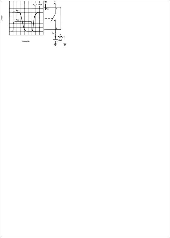
FIGURE 3. tON, tOFF Test Circuit and Waveforms for a Normally Open Switch
DS005667-41
FIGURE 4. ªOFFº Isolation, Crosstalk, Small Signal Response
Typical Performance Characteristics
ªONº Resistance |
ªONº Resistance |
ªONº Resistance |
DS005667-23 |
DS005667-24 |
DS005667-25 |
|
|
www.national.com |
6 |
 Loading...