


N November 1998
CLC446
400MHz, 50mW Current-Feedback Op Amp
General Description
The National CLC446 is a very high-speed unity-gain-stable cur- rent-feedback op amp that is designed to deliver the highest levels of performance from a mere 50mW quiescent power. It provides a very wide 400MHz bandwidth, a 2000V/ s slew rate and 900ps rise/fall times. The CLC446 achieves its superior speed- vs-power using an advanced complementary bipolar IC process and National’s current-feedback architecture.
The CLC446 is designed to drive video loads with very low differential gain and phase errors (0.02%, 0.03°). Combined with its very low power (50mW), the CLC446 makes an excellent choice for NTSC/PAL video switchers and routers. With its very quick edge rates (900ps) and high slew rate (2000V/ s), the CLC446 also makes an excellent choice for high-speed, highresolution component RGB video systems.
The CLC446 makes an excellent low-power high-resolution A/D converter driver with its very fast 9ns settling time (to 0.1%) and low harmonic distortion.
The combination of high performance and low power make the CLC446 useful in many high-speed general purpose applications. Its current-feedback architecture maintains consistent performance over a wide gain range and signal levels. DC gain and bandwidth can be set independently. Also, either maximally flat AC response or linear phase response can be emphasized.
Features
■400MHz bandwidth (Av = +2)
■5mA supply current
■0.02%, 0.03° differential gain, phase
■2000V/ s slew rate
■9ns settling to 0.1%
■0.05dB gain flatness to 100MHz
■-65/-78dBc HD2/HD3
Applications
■High resolution video
■A/D driver
■Medical imaging
■Video switchers & routers
■RF/IF amplifier
■Communications
■Instrumentation
Non-Inverting
Frequency Response (Av = +2)
8
Vo = 0.5Vpp
6
(dB) |
4 |
|
|
|
|
|
|
Gain |
2 |
|
|
|
|
|
|
|
|
|
|
|
|
|
|
|
0 |
|
|
|
|
|
|
|
|
|
|
|
|
|
|
|
-2 |
|
|
|
|
|
|
|
|
|
|
|
|
|
|
|
|
|
10M |
100M |
|
|
|
|
1M |
1G |
|||||
Frequency (Hz)
400MHz, |
CLC446 |
Amp Op Feedback-Current 50mW |
|
|
Typical Application |
|
Pinout |
||
|
Elliptic-Function Low Pass Filter |
|
DIP & SOIC |
||
R1 |
R2 |
C1 |
|
|
|
Vin |
|
|
+ |
|
VCC |
|
|
|
Vo |
||
|
C2 |
R4 |
CLC446 |
R5 |
|
C3 |
- |
|
|||
C4 |
|
C5 |
VEE |
||
|
|
|
|
||
R3 |
|
|
Rf |
|
|
|
|
|
|
|
|
|
|
|
Rg |
|
|
© 1998 National Semiconductor Corporation |
|
|
|
http://www.national.com |
|
Printed in the U.S.A.

Electrical Characteristics (AV = +2, Rf = 249Ω: VCC = + 5V, RL = 100Ω; unless specified)
PARAMETERS |
|
CONDITIONS |
TYP |
MIN/MAX RATINGS |
UNITS |
NOTES |
||
Ambient Temperature |
CLC446AJ |
+25˚C |
+25˚C |
0 to 70˚C |
-40 to 85˚C |
|
|
|
FREQUENCY DOMAIN RESPONSE |
|
|
|
|
|
|
||
-3dB bandwidth |
|
Vo < 0.2Vpp |
400 |
340 |
300 |
300 |
MHz |
|
gain flatness |
Vo < 2.0Vpp |
Vo < 2.0Vpp |
280 |
210 |
190 |
190 |
MHz |
|
<100MHz |
±0.05 |
±0.2 |
±0.2 |
±0.2 |
dB |
|
||
linear phase dev. Vo < 2.0Vpp |
<100MHz |
0.2 |
0.5 |
0.8 |
0.8 |
deg |
|
|
differential gain |
|
NTSC, RL=150Ω |
0.02 |
0.04 |
0.04 |
0.04 |
% |
|
differential phase |
|
NTSC, RL=150Ω |
0.03 |
0.05 |
0.05 |
0.05 |
deg |
|
TIME DOMAIN RESPONSE |
|
|
|
|
|
|
|
|
rise and fall time |
|
2V step |
0.9 |
1.4 |
1.5 |
1.6 |
ns |
|
settling time to 0.1% |
2V step |
9 |
13 |
15 |
15 |
ns |
|
|
overshoot |
|
2V step |
6 |
15 |
18 |
18 |
% |
|
slew rate |
|
2V step, ±0.5V crossing |
2000 |
1400 |
1300 |
1200 |
V/µs |
|
DISTORTION AND NOISE RESPONSE |
|
|
|
|
|
|
||
2nd harmonic distortion |
2V , 5MHz |
-65 |
-59 |
-58 |
-58 |
dBc |
|
|
|
|
pp |
|
|
|
|
|
|
|
|
2Vpp, 20MHz |
-55 |
-48 |
-48 |
-48 |
dBc |
|
3rd harmonic distortion |
2Vpp, 50MHz |
-54 |
-43 |
-42 |
-42 |
dBc |
|
|
2V , 5MHz |
-78 |
-70 |
-68 |
-68 |
dBc |
|
||
|
|
pp |
|
|
|
|
|
|
|
|
2Vpp, 20MHz |
-70 |
-62 |
-60 |
-60 |
dBc |
|
equivalent input noise |
2Vpp, 50MHz |
-50 |
-45 |
-42 |
-42 |
dBc |
|
|
|
|
|
|
|
nV/√Hz |
|
||
voltage (eni) |
|
>1MHz |
3.8 |
4.8 |
5.0 |
5.1 |
|
|
non-inverting current (ibn) |
>1MHz |
2.0 |
2.6 |
2.8 |
3.3 |
pA/√Hz |
|
|
inverting current (ibi) |
>1MHz |
16 |
19 |
20 |
21 |
pA/√Hz |
|
|
STATIC DC PERFORMANCE |
|
|
|
|
|
|
|
|
input offset voltage |
|
2 |
7 |
10 |
11 |
mV |
A |
|
average drift |
|
|
17 |
– |
25 |
35 |
µV/˚C |
|
input bias current |
|
non-inverting |
3 |
12 |
25 |
25 |
µA |
A |
average drift |
|
|
30 |
– |
90 |
130 |
nA/˚C |
|
input bias current |
|
inverting |
10 |
22 |
30 |
35 |
µA |
A |
average drift |
|
|
26 |
– |
75 |
85 |
nA/˚C |
|
power supply rejection ratio |
DC |
52 |
45 |
43 |
43 |
dB |
|
|
common-mode rejection ratio |
DC |
48 |
44 |
42 |
42 |
dB |
|
|
supply current |
|
RL= ∞ |
4.8 |
5.8 |
6.2 |
6.2 |
mA |
A |
MISCELLANEOUS PERFORMANCE |
|
|
|
|
MΩ |
|
||
input resistance |
|
non-inverting |
1.5 |
1.0 |
0.85 |
0.70 |
|
|
input capacitance |
|
non-inverting |
1 |
2 |
2 |
2 |
pF |
|
input range |
|
common-mode |
±2.8 |
±2.6 |
±2.4 |
±2.3 |
V |
|
output voltage range |
RL = 100Ω |
±3.1 |
±2.8 |
±2.8 |
±2.6 |
V |
|
|
output current |
|
RL = ∞ |
±3.2 |
±3.0 |
±2.9 |
±2.8 |
V |
|
|
|
48 |
48 |
48 |
48 |
mA |
|
|
output resistance, closed loop |
DC |
0.04 |
0.1 |
0.1 |
0.1 |
Ω |
|
|
|
|
|
|
|
|
|
|
|
|
|
|
|
|
|
|
|
|
Min/max ratings are based on product characterization and simulation. Individual parameters are tested as noted. Outgoing quality levels are determined from tested parameters.
Absolute Maximum Ratings
supply voltage |
±6V |
output current |
±48mA |
common-mode input voltage |
±Vcc |
maximum junction temperature |
+175˚C |
storage temperature range |
-65˚C to +150˚C |
lead temperature (soldering 10 sec) |
+300˚C |
ESD rating (human body model) |
1000V |
Notes
A) J-level: spec is 100% tested at +25˚C.
Ordering Information
Model |
|
Temperature Range |
|
Description |
|
|
|
|
|
CLC446AJP |
|
-40˚C to +85˚C |
|
8-pin PDIP |
CLC446AJE |
|
-40˚C to +85˚C |
|
8-pin SOIC |
CLC446ALC |
|
-40˚C to +85˚C |
|
dice |
CLC446A8B |
|
-55˚C to +125˚C |
|
8-pin CerDIP, MIL-STD-883 |
CLC446AMC |
|
-55˚C to +125˚C |
|
dice, MIL-STD-883 |
|
|
Contact the factory for other packages and DESC SMD number.
Package Thermal Resistance
Package |
|
θJC |
|
θJA |
Plastic (AJP) |
|
70˚C/W |
|
125˚C/W |
Surface Mount (AJE) |
|
60˚C/W |
|
140˚C/W |
Ceramic (A8B) |
|
40˚C/W |
|
130˚C/W |
|
|
Reliability Information
Transistor Count |
36 |
MTBF (based on limited test data) |
39Mhr |
http://www.national.com |
2 |

Typical Performance Characteristics (VCC = ±5V,Av = +2,Rf =249Ω, RL = 100Ω; unless specified)
Non-Inverting Frequency Response Inverting Frequency Response Frequency Response vs. RL
(1dB/div) |
Vo = 0.5Vpp |
Av = 1V/V |
|
(1dB/div) |
|
Av = 2V/V |
|||
|
Rf = 453Ω |
|||
|
|
Rf = 249Ω |
||
|
|
(deg)Phase |
||
Magnitude |
|
|
0 |
Magnitude |
Av = 10V/V |
-90 |
|||
Normalized |
|
Normalized |
||
Rf = 200Ω |
-180 |
|||
|
Av = 5V/V |
-270 |
||
|
-360 |
|||
|
Rf = 200Ω |
|||
|
|
-450 |
||
|
|
|
|
|
1M |
10M |
100M |
1G |
|
|
Vo = 0.5Vpp |
Av = -1V/V |
|
(1dB/div) |
|
|
Av = -2V/V |
||
|
|
Rf = 249Ω |
||
|
|
Rf = 249Ω |
||
|
|
|
||
|
|
|
(deg)Phase |
|
|
|
|
-180 |
Magnitude |
|
|
|
-225 |
|
|
|
Av = -5V/V |
-270 |
Normalized |
|
|
Rf = 200Ω |
-315 |
|
|
|
Av = -10V/V |
||
|
|
-360 |
||
|
|
Rf = 200Ω |
||
|
|
|
|
|
1M |
10M |
100M |
1G |
|
|
Vo = 0.5Vpp |
|
(deg) Phase |
|
|
RL = 1kΩ |
|
|
|
|
|
|
|
|
0 |
|
|
|
-90 |
|
|
RL = 100Ω |
-180 |
|
|
-270 |
|
|
|
RL = 500Ω |
|
|
|
-360 |
|
|
|
|
|
|
|
|
-450 |
1M |
10M |
100M |
1G |
Frequency (Hz) |
Frequency (Hz) |
Frequency (Hz) |
Frequency Response vs. Vo
(1dB/div) |
|
0.1Vpp |
|
|
|
1Vpp |
|
|
|
|
|
Magnitude |
|
4Vpp |
|
|
2Vpp |
|
|
Normalized |
|
|
|
|
|
|
|
1M |
10M |
100M |
1G |
Frequency (Hz)
Small Signal Pulse Response
|
(0.5V/div)Voltage |
|
|
|
|
|
|
|
|
|
|
|
|
|
|
|
|
|
|
|
|
|
|
|
|
|
|
|
|
|
|
|
|
|
|
|
|
|
|
|
|
|
|
|
|
|
|
|
|
|
|
|
|
|
|
|
|
|
|
|
|
|
|
|
|
|
|
|
|
|
|
|
|
|
|
|
|
|
|
|
|
|
|
|
|
|
|
|
|
|
|
|
|
|
|
|
|
|
|
|
|
|
|
|
|
|
|
|
|
Av = +2V/V |
|
|
|
|
|
|
|
|
|
|
|||||||
|
Output |
|
|
|
|
|
|
|
|
|
|
|
|
|
|
|
|
|
|
|
|
|
|
|
|||||||
|
|
|
|
|
|
|
|
|
|
|
|
|
|
|
|
|
|
|
|
|
|
|
|
|
|
|
|
|
|
|
|
|
|
|
|
|
|
|
|
|
|
|
|
|
|
|
|
|
|
|
|
|
|
|
|
|
|
|
|
|
|
|
|
|
|
|
|
|
|
|
|
|
|
|
|
|
|
|
|
|
|
|
|
|
|
|
|
|
|
|
|
|
|
|
|
|
|
|
|
|
|
|
|
|
|
|
|
|
|
|
|
|
|
|
|
|
|
|
|
|
|
|
|
|
|
|
|
|
|
|
|
|
|
|
|
|
|
|
|
|
|
|
|
|
|
|
|
|
|
|
|
|
|
|
|
|
|
|
|
|
|
|
|
|
|
|
|
|
|
|
|
|
|
|
|
|
|
|
|
|
|
|
|
|
|
|
|
|
|
|
|
|
|
|
|
|
|
|
|
|
|
|
|
|
|
|
|
|
|
|
|
|
|
|
|
|
|
|
|
|
|
|
|
|
|
|
|
|
|
|
|
|
|
|
|
|
|
Av = -2V/V |
|
|
|
|
|
|
|
|
|
|
|
||||||
|
|
|
|
|
|
|
|
|
|
|
|
|
|
|
|
|
|
|
|
|
|
|
|
|
|
||||||
|
|
|
|
|
|
|
|
|
|
|
|
|
|
|
|
|
|
|
|
|
|
|
|
|
|
|
|
|
|
|
|
|
|
|
|
|
|
|
|
|
|
|
|
|
|
|
|
|
|
|
|
|
|
|
|
|
|
|
|
|
|
|
|
|
|
|
|
|
|
|
|
|
|
|
|
|
|
|
|
|
|
|
|
|
|
|
|
|
|
|
|
|
|
|
|
|
|
|
|
|
|
|
|
|
|
|
|
Time (2ns/div) |
|||||||||||||||||||
|
|
2nd Harmonic Distortion |
|
|
|
|
|
|
|
|
|
|
|||||||||||||||||||
|
-50 |
|
|
|
|
|
|
|
|
|
|
|
|
|
|
|
|
|
|
|
|
|
|
|
|
|
|
|
|
|
|
|
|
|
|
Vo = 2Vpp |
|
|
|
|
|
|
|
|
|
|
|
|
|
|
|
|
|
|
|
|
|
|
|||||
(dBc) |
-60 |
|
|
|
|
|
|
|
|
|
|
|
|
|
|
|
|
|
|
|
|
|
|
|
|
|
|
|
|
|
|
|
|
|
|
|
|
|
|
|
|
|
|
|
|
|
|
|
|
|
|
|
|
|
|
|
|
|
|
|
|
||
-70 |
|
|
|
|
|
|
|
|
|
|
|
|
|
|
|
|
|
|
|
|
|
|
|
|
|
|
|
|
|
|
|
|
|
|
|
|
2nd RL |
= 100Ω |
|
|
|
|
|
|
|
|
|
|
|
|
|
|
|
|
|
|
|||||||
Distortion |
-80 |
|
|
|
|
|
|
|
|
|
|
|
|
|
|
|
|
|
|
|
|
|
|
|
|
|
|
|
|
|
|
|
|
|
|
|
|
|
|
|
|
|
|
|
|
|
|
|
|
|
|
|
|
|
|
|
|
|
|
|
|
||
|
|
|
|
|
|
|
|
|
|
|
|
|
|
|
|
|
|
|
|
|
|
|
|
|
|
|
|
|
|
|
|
|
|
|
|
|
|
|
|
2nd |
|
RL = 1kΩ |
|
|
|
|
|
|
|
|
|
|
|
|
|
|
|
|
|
||||
|
-90 |
|
|
|
|
|
|
|
|
|
|
|
|
|
|
|
|
|
|
|
|
|
|
|
|
|
|
|
|
|
|
|
|
|
|
|
|
|
|
|
|
|
|
|
|
|
|
|
|
|
|
|
|
|
|
|
|
|
|
|
|
|
|
|
-100 |
|
|
|
|
|
|
|
|
|
|
|
|
|
|
|
|
|
|
|
|
|
|
|
|
|
|
|
|
|
|
|
|
|
|
|
|
|
|
|
|
|
|
|
|
|
|
|
|
|
|
|
|
|
|
|
|
|
|
|
|
|
|
|
|
|
|
|
|
|
|
|
|
|
|
|
|
|
|
|
|
|
|
|
|
|
|
|
|
|
|
|
|
|
|
|
|
1M |
|
|
|
|
|
|
|
|
|
|
|
|
|
|
|
|
10M |
||||||||||||
|
|
|
|
|
|
|
|
|
|
|
|
Frequency (Hz) |
|||||||||||||||||||
|
-40 |
|
2nd Harmonic Distortion vs. Pout |
||||||||||||||||||||||||||||
|
|
|
|
|
|
|
|
|
|
|
|
|
|
|
|
|
|
|
|
|
|
|
|
|
|
|
|
|
|
|
|
|
|
|
|
|
|
|
|
|
|
|
|
|
|
|
|
|
|
|
|
|
|
|
|
|
|
|
|
|
|
|
|
|
|
|
|
|
|
|
|
|
|
|
|
|
|
|
|
|
|
|
|
|
|
|
|
|
|
|
|
|
|
||
|
|
|
|
|
|
|
|
|
|
|
|
|
|
|
|
|
|
|
|
|
|
|
|
|
|
|
|
|
|
|
|
|
-50 |
|
|
|
|
|
|
|
|
|
|
|
|
|
|
|
|
|
|
|
|
|
10MHz |
|
|
|
|
||||
(dBc) |
|
|
|
|
|
|
|
|
|
|
|
|
|
|
|
|
|
|
|
|
|
|
|
|
|
|
|
|
|
|
|
|
|
|
|
|
|
|
|
|
|
|
|
|
|
|
|
|
|
|
|
|
|
|
5MHz |
|
|
|
|
|
|||
Distortion |
-60 |
|
|
|
|
|
|
|
|
|
|
|
|
|
|
|
|
|
|
|
|
|
|
|
|
|
|
|
|
|
|
|
|
|
|
|
|
|
|
|
|
|
|
|
|
|
|
|
|
|
|
|
|
|
|
|
|
|
|
|
|
|
|
|
|
|
|
|
|
|
|
|
|
|
|
|
|
|
|
|
|
|
|
|
|
|
|
2MHz |
|
|
|
|
|||
|
-70 |
|
|
|
|
|
|
|
|
|
|
|
|
|
|
|
|
|
|
|
|
|
|
|
|
|
|
|
|
|
|
|
|
|
|
|
|
|
|
|
|
|
|
|
|
|
|
|
|
|
|
|
|
|
|
|
|
|
|
|
|
|
|
|
|
|
|
|
|
|
|
|
|
|
|
|
|
|
|
|
|
|
|
|
|
|
|
1MHz |
|
|
|
|
|||
|
-80 |
|
|
|
|
|
|
|
|
|
|
|
|
|
|
|
|
|
|
|
|
|
|
|
|
|
|
|
|
|
|
|
|
|
|
|
|
|
|
|
|
|
|
|
|
|
|
|
|
|
|
|
|
|
|
|
|
|
|
|
|
|
|
|
|
|
|
|
|
|
|
|
|
|
|
|
|
|
|
|
|
|
|
|
|
|
|
|
|
|
|
|
|
|
|
|
|
-4 -2 |
0 |
2 |
|
4 |
|
|
6 |
8 10 12 |
|||||||||||||||||||||
|
|
|
|
|
|
|
|
|
|
Output Power (dBm) |
|||||||||||||||||||||
Frequency Response vs. CL
(1dB/div) |
|
|
|
|
|
|
50 |
|
|
CL = 10pF |
|
40 |
|||
|
|
Rs = 46.4Ω |
|
||||
|
|
|
|
||||
Magnitude |
|
|
|
CL = 22pF |
|
|
|
|
|
|
Rs = 33.2Ω |
) |
30 |
||
|
|
|
|
|
(Ω |
|
|
|
|
|
|
CL = 47pF |
s |
|
|
|
|
|
|
R |
|
||
|
|
|
|
Rs = 21Ω |
20 |
||
Normalized |
|
|
|
|
CL = 100pF |
|
|
+ |
|
Rs |
|
Rs = 13.3Ω |
|
|
|
|
|
|
|
10 |
|||
- |
249Ω |
CL |
|
1k |
|
||
|
|
|
|
|
|
||
249Ω |
|
|
|
|
|
|
|
|
|
|
|
|
|
0 |
|
|
|
|
|
|
|
|
|
|
1M |
|
|
10M |
100M |
1G |
|
Recommended Rs vs. CL
10 |
20 |
30 |
40 |
50 |
60 |
70 |
80 |
90 |
100 |
Frequency (Hz)
Large Signal Pulse Response
Voltage(1V/div) |
Av = +2V/V |
|
|
Output |
Av = -2V/V |
Time (2ns/div)
3rd Harmonic Distortion
|
-50 |
|
|
|
|
|
|
|
|
|
|
|
|
|
|
|
|
|
|
Vo = 2Vpp |
|
|
|
|
|
|
|
|
|
|
|
|
|
(dBc) |
-60 |
|
|
|
|
|
|
|
|
|
|
|
|
|
|
|
|
|
|
|
|
|
|
|
|
|
|
|
|
|
|
||
-70 |
|
|
|
|
|
|
|
|
|
|
|
|
|
|
|
|
|
|
|
|
|
|
|
|
|
|
|
|
|
|
|
||
|
|
|
|
|
|
|
|
|
|
|
|
|
|
|
||
Distortion |
|
|
|
|
|
|
|
|
|
|
|
|
|
|
|
|
-80 |
|
|
3rd RL = 100Ω |
|
|
|
|
|
|
|
|
|||||
|
|
|
|
|
|
|
|
|
|
|
|
|
|
|
|
|
|
|
|
|
|
|
|
|
|
|
|
|
|
|
|
|
|
|
-90 |
|
|
|
|
|
|
|
|
|
|
|
|
|
|
|
|
|
|
|
|
|
|
|
|
|
|
|
|
|
|
|
|
|
|
|
|
|
3rd RL |
= 1kΩ |
|
|
|
|
|
|
||||
|
|
|
|
|
|
|
|
|
|
|
|
|||||
|
-100 |
|
|
|
|
|
|
|
|
|
|
|
|
|
|
|
|
|
|
|
|
|
|
|
|
|
|
|
|
|
|
|
|
|
|
|
|
|
|
|
|
|
|
|
|
|
|
|
|
|
|
1M |
|
|
|
|
|
|
10M |
||||||||
Frequency (Hz)
3rd Harmonic Distortion vs. Pout
|
-65 |
|
|
|
|
|
|
|
|
|
-70 |
|
|
|
10MHz |
|
|
|
|
(dBc) |
-75 |
|
|
|
5MHz |
|
|
|
|
|
|
|
|
|
|
|
|
|
|
Distortion |
-80 |
|
|
|
|
|
|
|
|
-85 |
|
|
|
2MHz |
|
|
|
|
|
|
|
|
|
|
|
|
|
||
|
|
|
|
1MHz |
|
|
|
|
|
|
|
|
|
|
|
|
|
|
|
|
-90 |
|
|
|
|
|
|
|
|
|
-95 |
|
|
|
|
|
|
|
|
|
-4 |
-2 |
0 |
2 |
4 |
6 |
8 |
10 |
12 |
Output Power (dBm)
|
|
|
|
|
CL(pF) |
|
|
|
|
||
Equivalent Input Noise |
|
|
|
|
|||||||
100 |
|
|
|
|
|
|
|
|
|
|
100 |
NoiseVoltage(nV/ÖHz) |
|
|
|
|
|
|
|
|
|
|
Hz)(pA/NoiseÖ Current |
|
|
|
|
|
|
|
|
|
|
||
|
|
|
|
|
|
|
|
|
|
||
|
|
|
|
|
|
|
|
|
|
||
|
|
|
|
|
|
ibi |
|
|
|
||
10 |
|
|
|
|
|
|
|
|
|
|
|
|
|
|
|
|
|
|
|
|
|
10 |
|
|
|
|
|
|
|
|
|
|
|
|
|
|
|
|
|
|
|
|
|
|
|
|
|
|
|
|
|
|
|
|
|
|
|
|
|
|
|
|
|
|
|
|
|
|
|
|
|
|
|
|
|
|
|
|
|
|
|
|
|
|
|
|
|
|
|
|
|
|
|
|
|
|
|
|
|
|
|
|
eni |
|
|
|
|
|
|
|
|
|
|
|
ibn |
|
|
|
|
1 |
|
|
|
|
|
|
|
|
|
|
1 |
|
|
|
|
|
|
|
|
|
|
||
1k |
10k |
100k |
1M |
10M |
100M |
||||||
|
|
|
|
Frequency (Hz) |
|
|
|
|
|||
Differential Gain and Phase (3.58MHz)
|
0.01 |
|
|
0 |
|
Gain (%) |
0 |
|
Phase Pos Sync |
-0.04 |
Differential |
|
|
||||
-0.01 |
Phase Neg Sync |
|
-0.08 |
||
Differential |
|
|
|
(deg) Phase |
|
-0.02 |
Gain Pos Sync |
-0.12 |
|||
|
|
||||
-0.03 |
|
Gain Neg Sync |
-0.16 |
||
|
|
||||
|
-0.04 |
|
|
-0.2 |
|
|
1 |
2 |
3 |
4 |
|
Number of 150Ω Loads
|
Vos, IBN, & IBI vs. Temperature |
|
|
|
|||||
|
2 |
|
|
|
|
|
|
2 |
|
|
|
|
|
|
|
|
Vos |
|
|
|
|
|
|
|
|
|
|
|
I |
(mV) |
|
|
|
|
|
|
|
|
BI |
1 |
|
|
|
|
|
|
-2 |
I , |
|
|
|
|
|
|
IBN |
|
|
BN |
|
os |
|
|
|
|
|
|
|
|
( |
V |
|
|
|
|
|
|
|
|
A)m |
|
0 |
|
|
|
|
|
|
-6 |
|
|
|
|
|
|
|
IBI |
|
|
|
|
-1 |
|
|
|
|
|
|
-10 |
|
|
-60 |
-40 |
-20 |
0 |
20 |
40 |
60 |
80 |
|
Temperature (°C)
3 |
http://www.national.com |
Typical Performance Characteristics (VCC = ±5V, A v = +2, Rf = 249Ω, RL = 100Ω; unless specified)
Short Term Settling Time |
Long Term Settling Time |
|
0.2 |
|
|
VO = 2V step |
|
0.2 |
|
|
|
|
VO = 2V step |
|
|
Step) |
|
|
|
Step) |
|
|
|
|
|
|
|||
0.1 |
|
|
|
|
0.1 |
|
|
|
|
|
|
||
Output(% |
|
|
|
|
Output(% |
|
|
|
|
|
|
||
0 |
|
|
|
|
0 |
|
|
|
|
|
|
||
o |
-0.1 |
|
|
|
|
o |
-0.1 |
|
|
|
|
|
|
V |
|
|
|
|
V |
|
|
|
|
|
|
||
|
-0.2 |
|
|
|
|
|
-0.2 |
|
|
|
|
|
|
|
1n |
10n |
100n |
1μ |
10μ |
|
1μ |
10μ |
100μ |
1m |
10m |
100m |
1 |
Time (sec) |
Time (s) |
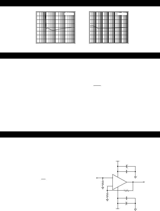
CLC446 Operation
The CLC446 has a current-feedback architecture built in an advanced complementary bipolar process. The key features of current-feedback are:
■AC bandwidth is independent of voltage gain
■Unity-gain stability
■Frequency response may be adjusted with Rf
■High slew rate
■Low variation in performance for a wide range of gains, signal levels and loads
■Fast settling
Current-feedback operation can be explained with a simple model. The voltage gain for the circuits in Figures 1 and 2 is approximately:
Vo |
= |
|
|
Av |
|
V |
1+ |
|
Rf |
||
in |
|
Z(jw) |
|||
|
|
|
|
||
where
■Av is the DC voltage gain
■Rf is the feedback resistor
■Z(jω) is the CLC446’s open-loop transimpedance gain
■Z(jw) is the loop-gain
Rf
The denominator of the equation above is approximately 1 at low frequencies. Near the -3dB corner frequency, the interaction between Rf and Z(jω) dominates the circuit performance. Increasing Rf does the following:
■Decreases loop-gain
■Decreases bandwidth
■Lowers pulse response overshoot
■Reduces gain peaking
■Affects frequency response phase linearity
CLC446 Design Information
The following topics will supply you with:
■Design parameters, formulas and techniques
■Interfaces
■Application circuits
■Layout techniques
■SPICE model information
DC Gain (non-inverting)
The non-inverting DC voltage gain for the configuration
shown in Figure 1 is Av = 1+ Rf . Rg
The normalized gain plots in the Typical Performance Characteristics section show different feedback resistors (Rf) for different gains. These values of Rf are recommended for obtaining the highest bandwidth with minimal peaking. The resistor Rt provides DC bias for the non-inverting input.
For Av < 5, use linear interpolation on the nearest Av values to calculate the recommended value of Rf. For Av ≥ 5, the minimum recommended Rf is 200Ω.
Select Rg to set the DC gain: Rg = |
Rf |
|
. |
||
Av |
- 1 |
||||
|
|
||||
DC gain accuracy is usually limited by the tolerance of Rf and Rg.
VCC
|
|
|
|
6.8mF |
|
|
|
|
|
|
|
+ |
|
Vin |
|
3 |
7 |
0.1mF |
|
|
|
|
|
+ |
|
6 |
Vo |
|
Rt |
|
CLC446 |
|||
|
2 |
|
|
|||
|
- |
|
|
|
||
|
|
|
|
|
||
|
|
|
|
Rf |
|
|
|
|
|
4 |
|
|
|
|
|
Rg |
|
0.1mF |
|
|
|
|
|
|
|
+ |
|
6.8mF
VEE
Fi
Figure 1: Non-Inverting Gain
http://www.national.com |
4 |
 Loading...