


NSC LF356N, LF356M, LF356H, LF356BH, LF155H Datasheet
...May 2000
LF155/LF156/LF355/LF356/LF357
JFET Input Operational Amplifiers
General Description
These are the first monolithic JFET input operational amplifiers to incorporate well matched, high voltage JFETs on the same chip with standard bipolar transistors (BI-FET™ Technology). These amplifiers feature low input bias and offset currents/low offset voltage and offset voltage drift, coupled with offset adjust which does not degrade drift or common-mode rejection. The devices are also designed for high slew rate, wide bandwidth, extremely fast settling time, low voltage and current noise and a low 1/f noise corner.
Advantages
nReplace expensive hybrid and module FET op amps
nRugged JFETs allow blow-out free handling compared with MOSFET input devices
nExcellent for low noise applications using either high or low source impedance Ð very low 1/f corner
nOffset adjust does not degrade drift or common-mode rejection as in most monolithic amplifiers
nNew output stage allows use of large capacitive loads (5,000 pF) without stability problems
nInternal compensation and large differential input voltage capability
Applications
nPrecision high speed integrators
nFast D/A and A/D converters
nHigh impedance buffers
nWideband, low noise, low drift amplifiers
nLogarithmic amplifiers
nPhotocell amplifiers
nSample and Hold circuits
Common Features
nLow input bias current: 30pA
nLow Input Offset Current: 3pA
nHigh input impedance: 1012Ω
n Low input noise current:
nHigh common-mode rejection ratio: 100 dB
nLarge dc voltage gain: 106 dB
Uncommon Features
|
|
LF155/ |
LF156/ |
LF357 |
Units |
|
|
LF355 |
LF356 |
(AV=5) |
|
j |
Extremely |
4 |
1.5 |
1.5 |
µs |
|
fast settling |
|
|
|
|
|
time to |
|
|
|
|
|
0.01% |
|
|
|
|
j |
Fast slew |
5 |
12 |
50 |
V/µs |
|
rate |
|
|
|
|
j |
Wide gain |
2.5 |
5 |
20 |
MHz |
|
bandwidth |
|
|
|
|
j |
Low input |
20 |
12 |
12 |
|
|
noise |
|
|
|
|
|
voltage |
|
|
|
|
Simplified Schematic
DS005646-1
*3 pF in LF357 series.
BI-FET™ , BI-FET II™ are trademarks of National Semiconductor Corporation.
Amplifiers Operational Input JFET LF155/LF156/LF355/LF356/LF357
© 2000 National Semiconductor Corporation |
DS005646 |
www.national.com |

LF155/LF156/LF355/LF356/LF357
Absolute Maximum Ratings (Note 1)
If Military/Aerospace specified devices are required, contact the National Semiconductor Sales Office/Distributors for availability and specifications.
|
LF155/6 |
LF356B |
LF355/6/7 |
Supply Voltage |
±22V |
±22V |
±18V |
Differential Input Voltage |
±40V |
±40V |
±30V |
Input Voltage Range (Note 2) |
±20V |
±20V |
±16V |
Output Short Circuit Duration |
Continuous |
Continuous |
Continuous |
TJMAX |
|
|
|
H-Package |
150ÊC |
115ÊC |
115ÊC |
N-Package |
|
100ÊC |
100ÊC |
M-Package |
|
100ÊC |
100ÊC |
Power Dissipation at TA = 25ÊC (Notes 1, |
|
|
|
8) |
|
|
|
H-Package (Still Air) |
560 mW |
400 mW |
400 mW |
H-Package (400 LF/Min Air Flow) |
1200 mW |
1000 mW |
1000 mW |
N-Package |
|
670 mW |
670 mW |
M-Package |
|
380 mW |
380 mW |
Thermal Resistance (Typical) θJA |
|
|
|
H-Package (Still Air) |
160ÊC/W |
160ÊC/W |
160ÊC/W |
H-Package (400 LF/Min Air Flow) |
65ÊC/W |
65ÊC/W |
65ÊC/W |
N-Package |
|
130ÊC/W |
130ÊC/W |
M-Package |
|
195ÊC/W |
195ÊC/W |
(Typical) θJC |
|
|
|
H-Package |
23ÊC/W |
23ÊC/W |
23ÊC/W |
Storage Temperature Range |
−65ÊC to +150ÊC |
−65ÊC to +150ÊC |
−65ÊC to +150ÊC |
Soldering Information (Lead Temp.) |
|
|
|
Metal Can Package |
|
|
|
Soldering (10 sec.) |
300ÊC |
300ÊC |
300ÊC |
Dual-In-Line Package |
|
|
|
Soldering (10 sec.) |
260ÊC |
260ÊC |
260ÊC |
Small Outline Package |
|
|
|
Vapor Phase (60 sec.) |
|
215ÊC |
215ÊC |
Infrared (15 sec.) |
|
220ÊC |
220ÊC |
See AN-450 ªSurface Mounting Methods and Their Effect on Product Reliabilityº for other methods of soldering surface mount devices.
ESD tolerance |
|
|
|
(100 pF discharged through 1.5 kΩ) |
1000V |
1000V |
1000V |
DC Electrical Characteristics
(Note 3)
Symbol |
Parameter |
|
Conditions |
|
LF155/6 |
|
|
LF356B |
|
LF355/6/7 |
Units |
|||||
|
|
|
|
|
|
|
|
|
|
|
|
|||||
|
Min |
Typ |
|
Max |
Min |
Typ |
|
Max |
Min |
Typ |
Max |
|||||
|
|
|
|
|
|
|
|
|||||||||
|
|
|
|
|
|
|
|
|
|
|
|
|
|
|
|
|
VOS |
|
Input Offset Voltage |
RS=50Ω, TA=25ÊC |
|
3 |
|
5 |
|
3 |
|
5 |
|
3 |
10 |
mV |
|
|
|
|
Over Temperature |
|
|
|
7 |
|
|
|
6.5 |
|
|
13 |
mV |
|
|
|
|
|
|
|
|
|
|
|
|
|
|
|
|
|
|
VOS/ |
T |
Average TC of Input |
RS=50Ω |
|
5 |
|
|
|
5 |
|
|
|
5 |
|
µV/ÊC |
|
|
|
Offset Voltage |
|
|
|
|
|
|
|
|
|
|
||||
|
|
|
|
|
|
|
|
|
|
|
|
|
|
|
|
|
|
|
|
|
|
|
|
|
|
|
|
|
|
|
|
|
|
TC/ |
VOS |
Change in Average TC |
RS=50Ω, (Note 4) |
|
0.5 |
|
|
|
0.5 |
|
|
|
0.5 |
|
µV/ÊC |
|
|
|
with VOS Adjust |
|
|
|
|
|
|
|
|
|
|
per mV |
|||
|
|
|
|
|
|
|
|
|
|
|
|
|
|
|
||
IOS |
|
Input Offset Current |
TJ=25ÊC, (Notes 3, 5) |
|
3 |
|
20 |
|
3 |
|
20 |
|
3 |
50 |
pA |
|
|
|
|
TJ≤THIGH |
|
|
|
20 |
|
|
|
1 |
|
|
2 |
nA |
|
IB |
|
Input Bias Current |
TJ=25ÊC, (Notes 3, 5) |
|
30 |
|
100 |
|
30 |
|
100 |
|
30 |
200 |
pA |
|
|
|
|
TJ≤THIGH |
|
|
|
50 |
|
|
|
5 |
|
|
8 |
nA |
|
R |
|
Input Resistance |
T |
=25ÊC |
|
1012 |
|
|
|
1012 |
|
|
|
1012 |
|
Ω |
IN |
|
|
J |
|
|
|
|
|
|
|
|
|
|
|
|
|
www.national.com |
2 |

DC Electrical Characteristics (Continued)
(Note 3)
Symbol |
Parameter |
Conditions |
|
LF155/6 |
|
LF356B |
|
|
LF355/6/7 |
Units |
||||
|
|
|
|
|
|
|
|
|
|
|
||||
Min |
Typ |
Max |
Min |
Typ |
|
Max |
Min |
|
Typ |
Max |
||||
|
|
|
|
|
|
|||||||||
|
|
|
|
|
|
|
|
|
|
|
|
|
|
|
AVOL |
Large Signal Voltage |
VS=±15V, TA=25ÊC |
50 |
200 |
|
50 |
200 |
|
|
25 |
|
200 |
|
V/mV |
|
Gain |
VO=±10V, RL=2k |
|
|
|
|
|
|
|
|
|
|
|
|
|
|
Over Temperature |
25 |
|
|
25 |
|
|
|
15 |
|
|
|
V/mV |
|
|
|
|
|
|
|
|
|
|
|
|
|
|
|
VO |
Output Voltage Swing |
VS=±15V, RL=10k |
±12 |
±13 |
|
±12 |
±13 |
|
|
±12 |
|
±13 |
|
V |
|
|
VS=±15V, RL=2k |
±10 |
±12 |
|
±10 |
±12 |
|
|
±10 |
|
±12 |
|
V |
VCM |
Input Common-Mode |
VS=±15V |
±11 |
+15.1 |
|
±11 |
±15.1 |
|
|
+10 |
|
+15.1 |
|
V |
|
Voltage Range |
|
−12 |
|
−12 |
|
|
|
−12 |
|
V |
|||
|
|
|
|
|
|
|
|
|
|
|||||
|
|
|
|
|
|
|
|
|
|
|
|
|
|
|
CMRR |
Common-Mode |
|
85 |
100 |
|
85 |
100 |
|
|
80 |
|
100 |
|
dB |
|
Rejection Ratio |
|
|
|
|
|
|
|||||||
|
|
|
|
|
|
|
|
|
|
|
|
|
|
|
|
|
|
|
|
|
|
|
|
|
|
|
|
|
|
PSRR |
Supply Voltage |
(Note 6) |
85 |
100 |
|
85 |
100 |
|
|
80 |
|
100 |
|
dB |
|
Rejection Ratio |
|
|
|
|
|
|
|||||||
|
|
|
|
|
|
|
|
|
|
|
|
|
|
|
|
|
|
|
|
|
|
|
|
|
|
|
|
|
|
DC Electrical Characteristics
TA = TJ = 25ÊC, VS = ±15V
Parameter |
|
LF155 |
|
LF355 |
LF156/356B |
|
LF356 |
|
LF357 |
Units |
|||||
|
|
|
|
|
|
|
|
|
|
|
|
|
|
||
Typ |
|
Max |
Typ |
|
Max |
Typ |
Max |
Typ |
|
Max |
Typ |
|
Max |
||
|
|
|
|
|
|
||||||||||
|
|
|
|
|
|
|
|
|
|
|
|
|
|
|
|
Supply |
2 |
|
4 |
2 |
|
4 |
5 |
7 |
5 |
|
10 |
5 |
|
10 |
mA |
Current |
|
|
|
|
|||||||||||
|
|
|
|
|
|
|
|
|
|
|
|
|
|
|
|
|
|
|
|
|
|
|
|
|
|
|
|
|
|
|
|
AC Electrical Characteristics
TA = TJ = 25ÊC, VS = ±15V
|
|
|
LF155/355 |
LF156/356B |
LF156/356/ |
LF357 |
|
Symbol |
Parameter |
Conditions |
|
|
LF356B |
|
Units |
|
|
|
Typ |
Min |
Typ |
Typ |
|
|
|
|
|
|
|
|
|
SR |
Slew Rate |
LF155/6: AV=1, |
5 |
7.5 |
12 |
|
V/µs |
|
|
LF357: AV=5 |
|
|
|
50 |
V/µs |
GBW |
Gain Bandwidth |
|
2.5 |
|
5 |
20 |
MHz |
|
Product |
|
|
||||
|
|
|
|
|
|
|
|
|
|
|
|
|
|
|
|
ts |
Settling Time to 0.01% |
(Note 7) |
4 |
|
1.5 |
1.5 |
µs |
en |
Equivalent Input Noise |
RS=100Ω |
|
|
|
|
|
|
Voltage |
f=100 Hz |
25 |
|
15 |
15 |
|
|
|
f=1000 Hz |
20 |
|
12 |
12 |
|
|
|
|
|
|
|
|
|
in |
Equivalent Input |
f=100 Hz |
0.01 |
|
0.01 |
0.01 |
|
|
Current Noise |
f=1000 Hz |
0.01 |
|
0.01 |
0.01 |
|
|
|
|
|
|
|
|
|
CIN |
Input Capacitance |
|
3 |
|
3 |
3 |
pF |
Notes for Electrical Characteristics
Note 1: The maximum power dissipation for these devices must be derated at elevated temperatures and is dictated by TJMAX, θJA, and the ambient temperature, TA. The maximum available power dissipation at any temperature is Pd=(TJMAX−T A)/θJA or the 25ÊC PdMAX, whichever is less.
Note 2: Unless otherwise specified the absolute maximum negative input voltage is equal to the negative power supply voltage.
Note 3: Unless otherwise stated, these test conditions apply:
|
|
LF155/156 |
LF356B |
LF355/6/7 |
|
|
|
|
|
Supply Voltage, VS |
|
±15V≤VS≤±20V |
±15V≤VS±20V |
VS=±15V |
TA |
|
−55ÊC ≤TA≤+125ÊC |
0ÊC ≤TA≤+70ÊC |
0ÊC ≤TA≤+70ÊC |
THIGH |
|
+125ÊC |
+70ÊC |
+70ÊC |
and VOS, IB and IOS are measured at VCM=0. |
|
|
|
|
Note 4: The Temperature Coefficient of the adjusted input offset voltage changes only a small amount (0.5µV/ÊC typically) for each mV of adjustment from its o riginal unadjusted value. Common-mode rejection and open loop voltage gain are also unaffected by offset adjustment.
LF155/LF156/LF355/LF356/LF357
3 |
www.national.com |
LF155/LF156/LF355/LF356/LF357
Notes for Electrical Characteristics (Continued)
Note 5: The input bias currents are junction leakage currents which approximately double for every 10ÊC increase in the junction temperature, TJ. Due to limited production test time, the input bias currents measured are correlated to junction temperature. In normal operation the junction temperature rises above the ambient temperature as a result of internal power dissipation, Pd. TJ=TA+θJA Pd where θJA is the thermal resistance from junction to ambient. Use of a heat sink is recommended if input bias current is to be kept to a minimum.
Note 6: Supply Voltage Rejection is measured for both supply magnitudes increasing or decreasing simultaneously, in accordance with common practice.
Note 7: Settling time is defined here, for a unity gain inverter connection using 2 kΩ resistors for the LF155/6. It is the time required for the error voltage (the voltage at the inverting input pin on the amplifier) to settle to within 0.01% of its final value from the time a 10V step input is applied to the inverter. For the LF357, AV=−5, the feedback resistor from output to input is 2 kΩ and the output step is 10V (See Settling Time Test Circuit).
Note 8: Max. Power Dissipation is defined by the package characteristics. Operating the part near the Max. Power Dissipation may cause the part to operate outside guaranteed limits.
Typical DC Performance Characteristics Curves are for LF155 and LF156 unless otherwise specified.
Input Bias Current |
Input Bias Current |
DS005646-37 |
DS005646-38 |
Input Bias Current |
Voltage Swing |
DS005646-39 |
DS005646-40 |
www.national.com |
4 |
Typical DC Performance Characteristics Curves are for LF155 and LF156 unless otherwise specified. (Continued)
Supply Current |
Supply Current |
|
DS005646-41 |
DS005646-42 |
|
|
|
Negative Current Limit |
|
Positive Current Limit |
DS005646-43
DS005646-44
Positive Common-Mode |
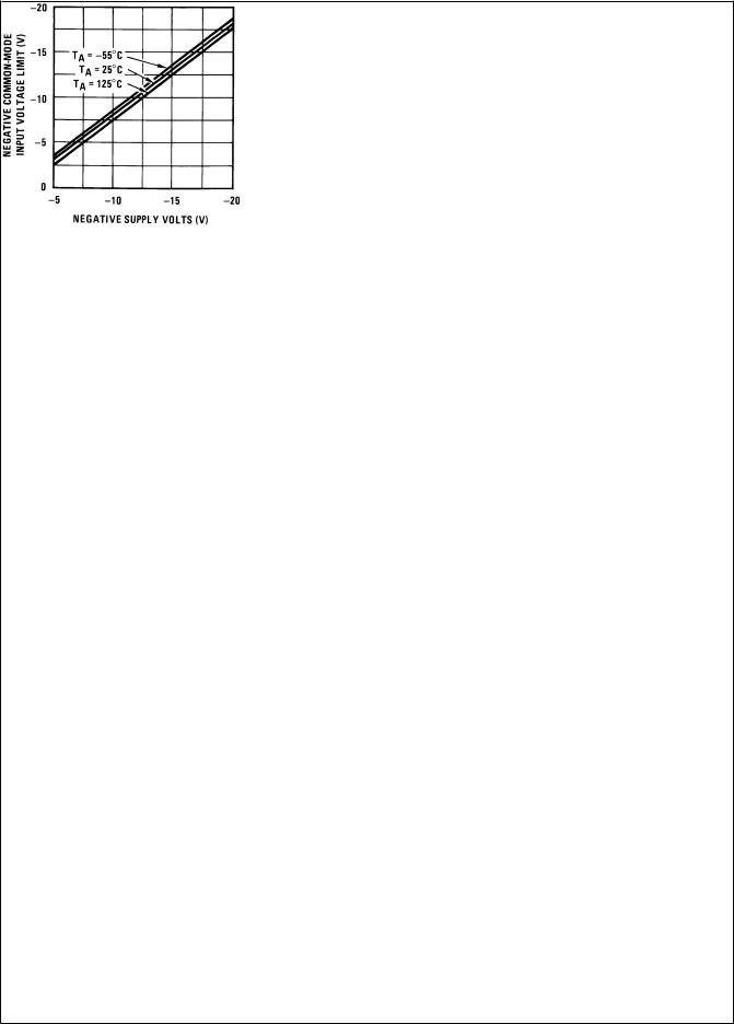
Negative Common-Mode |
Input Voltage Limit |
Input Voltage Limit |
DS005646-45
DS005646-46
LF155/LF156/LF355/LF356/LF357
5 |
www.national.com |
LF155/LF156/LF355/LF356/LF357
Typical DC Performance Characteristics Curves are for LF155 and LF156 unless otherwise specified. (Continued)
Open Loop Voltage Gain |
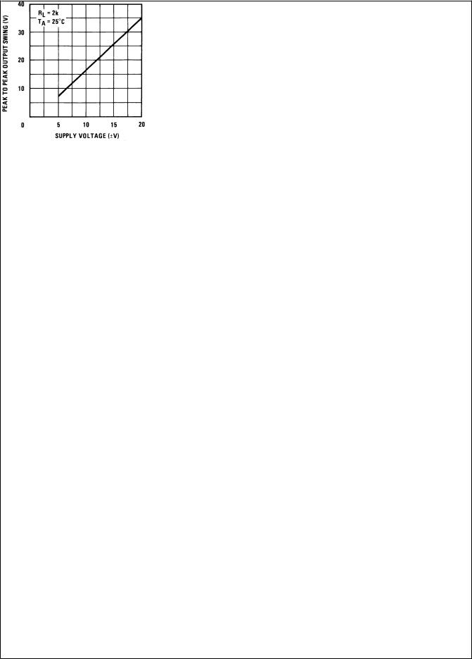
Output Voltage Swing |
DS005646-47 |
DS005646-48 |
Typical AC Performance Characteristics |
|
Gain Bandwidth |
Gain Bandwidth |
DS005646-50
|
DS005646-49 |
Normalized Slew Rate |
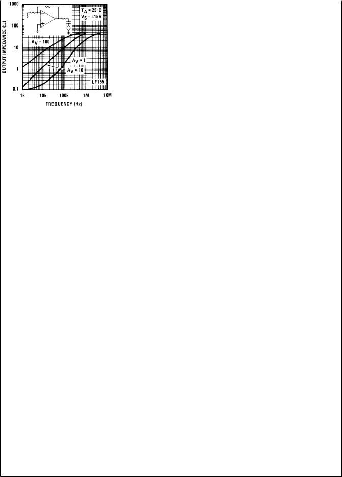
Output Impedance |
DS005646-51
DS005646-52
www.national.com |
6 |

Typical AC Performance Characteristics (Continued)
Output Impedance |
LF155 Small Signal Pulse Response, AV = +1 |
DS005646-5
DS005646-53
LF156 Small Signal Pulse Response, AV = +1 |
LF155 Large Signal Pulse Response, A = +1 |
|
V |
DS005646-6 DS005646-8
LF156 Large Signal Puls |
Inverter Settling Time |
|
Response, AV = +1 |
||
|
DS005646-9
DS005646-55
LF155/LF156/LF355/LF356/LF357
7 |
www.national.com |
LF155/LF156/LF355/LF356/LF357
Typical AC Performance Characteristics (Continued)
Inverter Settling Time |
Open Loop Frequency Response |
|
DS005646-56 |
|
DS005646-57 |
Bode Plot |
Bode Plot |
DS005646-58 DS005646-59
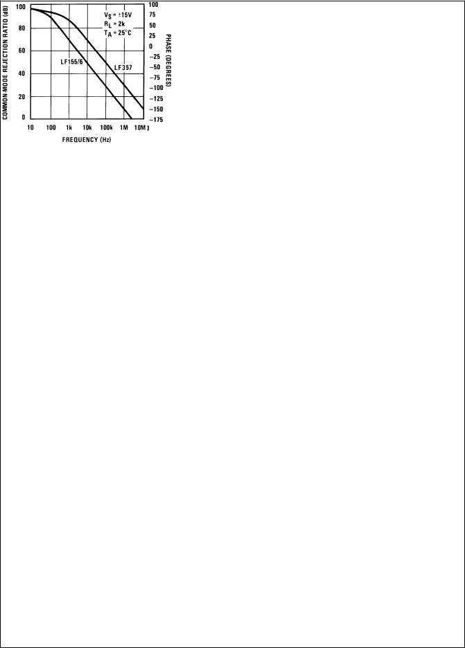
Bode Plot Common-Mode Rejection Ratio
DS005646-60 |
DS005646-61 |
www.national.com |
8 |
 Loading...