


NSC COPCH912-CDF-WM, COPCH912-AOF-N, COPCH912-ALG-WM, COPCH912-FGJ-WM, COPCH912-FGE-N Datasheet
...August 2000
COP912C
8-Bit Microcontroller
General Description
Note: COP8SA devices are instruction set and pinout compatible supersets of the COP912C devices, and are replacements for these in new designs when possible.
The COP912C ROM based microcontrollers are integrated COP8(tm) Base core devices with smaller memory (768 bytes), and fewer on-board features. These single-chip CMOS devices are suited for lower-functionality applications where system cost is of prime consideration. Pin and software compatible (different Vcc range) 4k/32k OTP versions are available (COP87LxxCJ/RJ Family). Erasable windowed versions are available for use with a range of COP8(tm) software and hardware development tools.
Family features include an 8-bit memory mapped architecture, 10MHz CKI with 2.5us(912C) or 2us(912CH) instruction cycle, one multi-function 16-bit timer/counter with PWM, MICROWIRE/PLUS(tm) serial I/O, power saving HALT mode, three clock modes, high current outputs, software selectable I/O options, multi-volt operation and 20 pin packages.
Devices included in this datasheet are:
Device |
Memory (bytes) |
RAM |
I/O Pins |
Packages |
Temperature |
Comments |
|
(bytes) |
|||||||
|
|
|
|
|
|
||
|
|
|
|
|
|
|
|
COP912C |
768 ROM |
64 |
16 |
20 DIP/SOIC |
0 to +70ÊC |
2.3v - 4.0v |
|
COP912CH |
768ROM |
64 |
16 |
20 DIP/SOIC |
0 to +70ÊC |
4.0v - 5.5v |
|
|
|
|
|
|
|
|
Key Features
nLowest cost COP8 microcontroller
n16-bit multi-function timer supporting
ÐPWM mode
ÐExternal event counter mode
ÐInput capture mode
n768 bytes of ROM
n64 bytes of RAM
nVersatile and easy to use instruction set
n8-bit Stack Pointer (SP) Ð stack in RAM
nTwo 8-bit Register Indirect Memory Pointers (B, X)
Fully Static CMOS
nLow current drain (typically < 1 µA)
nSingle supply operation: 2.3V to 4.0V or 4.0V to 5.5V
nTemperature range: 0ÊC to +70ÊC
I/O Features
nMemory mapped I/O
nSoftware selectable I/O options (TRI-STATE® Output, Push-Pull Output, Weak Pull-Up Input, High Impedance Input)
nSchmitt trigger inputs on Port G
nMICROWIRE/PLUS™ Serial I/O
nPackages: 20 DIP/SO with 16 I/O pins
CPU/Instruction Set Features
nInstruction cycle time of 2 µs for COP912CH and 2.5 µs for COP912C
nThree multi-sourced interrupts servicing Ð External Interrupt with selectable edge Ð Timer interrupt
Ð Software interrupt
Development Support
nEmulation and OTP devices
nReal time emulation and full program debug offered by MetaLink Development System
Applications
nElectronic keys and switches
nRemote Control
nTimers
nAlarms
nSmall industrial control units
nLow cost slave controllers
nTemperature meters
nSmall domestic appliances
nToys and games
TRI-STATE® is a registered trademark of National Semiconductor Corporation.
COP8™ , MICROWIRE/PLUS™ , WATCHDOG™ and MICROWIRE™ are trademarks of National Semiconductor Corporation. PC® is a registered trademark of International Business Machines Corp.
iceMaster™ is a trademark of MetaLink Corporation.
Microcontroller Bit-8 COP912C
© 2000 National Semiconductor Corporation |
DS012060 |
www.national.com |

COP912C
Block Diagram
DS012060-1
www.national.com |
2 |

Absolute Maximum Ratings (Note 1)
If Military/Aerospace specified devices are required, please contact the National Semiconductor Sales Office/ Distributors for availability and specifications.
Supply Voltage (VCC) |
6.0V |
Voltage at Any Pin |
−0.3V to V CC +0.3V |
Total Current into VCC Pin (Source) |
80 mA |
Total Current out of GND Pin (Sink) |
80 mA |
Storage Temperature Range |
−65ÊC to +150ÊC |
Note 1: Absolute maximum ratings indicate limits beyond which damage to the device may occur. DC and AC electrical specifications are not ensured when operating the device at absolute maximum ratings.
DC Electrical Characteristics
COP912C/COP912CH; 0ÊC ≤ TA ≤ +70ÊC unless other specified
Parameter |
Conditions |
Min |
Typ |
Max |
Units |
|
|
|
|
|
|
Operating Voltage |
|
|
|
|
|
912C |
|
2.3 |
|
4.0 |
V |
912CH |
|
4.0 |
|
5.5 |
V |
Power Supply Ripple 1 (Note 2) |
Peak to Peak |
|
|
0.1 VCC |
V |
Supply Current (Note 3) |
|
|
|
|
|
CKI = 4 MHz |
VCC = 5.5V, tc = 2.5 µs |
|
|
6.0 |
mA |
CKI = 4 MHz |
VCC = 4.0V, tc = 2.5 µs |
|
|
2.5 |
mA |
HALT Current |
VCC = 5.5V, CKI = 0 MHz |
|
<1 |
8 |
µA |
INPUT LEVELS (VIH, VIL) |
|
|
|
|
|
Reset, CKI: |
|
|
|
|
|
Logic High |
|
0.9 VCC |
|
|
V |
Logic Low |
|
|
|
0.1 VCC |
V |
All Other Inputs |
|
|
|
|
|
Logic High |
|
0.7 VCC |
|
|
V |
Logic Low |
|
|
|
0.2 VCC |
V |
Hi-Z Input Leakage/TRI-STATE Leakage |
VCC = 5.5V |
−2 |
|
+2 |
µA |
Input Pullup Current |
VCC = 5.5V |
|
|
250 |
µA |
G-Port Hysteresis |
|
|
0.05 VCC |
0.35 VCC |
V |
Output Current Levels |
|
|
|
|
|
Source (Push-Pull Mode) |
VCC = 4.0V, VOH = 3.8V |
0.4 |
|
|
mA |
|
VCC = 2.3V, VOH = 1.8V |
0.2 |
|
|
mA |
Sink (Push-Pull Mode) |
VCC = 4.0V, VOL = 1.0V |
4.0 |
|
|
mA |
|
VCC = 2.3V, VOL = 0.4V |
0.7 |
|
|
mA |
Allowable Sink/Source Current Per Pin |
|
|
|
3 |
mA |
|
|
|
|
|
|
Input Capacitance (Note 4) |
|
|
|
7 |
pF |
|
|
|
|
|
|
Load Capacitance on D2 (Note 4) |
|
|
|
1000 |
pF |
|
|
|
|
|
|
Note 2: Rate of voltage change must be less then 0.5 V/ms.
Note 3: Supply current is measured after running 2000 cycles with a square wave CKI input, CKO open, inputs at rails and outputs open.
Note 4: Characterized, not tested.
DS012060-2
FIGURE 1. MICROWIRE/PLUS Timing
COP912C
3 |
www.national.com |
COP912C
Typical Performance Characteristics
Halt Ð IDD |
Dynamic Ð IDD (Crystal Clock Option) |
DS012060-16 DS012060-17
Port L/G Weak Pull-Up Source Current Port L/G Push-Pull Source Current
DS012060-18 DS012060-19
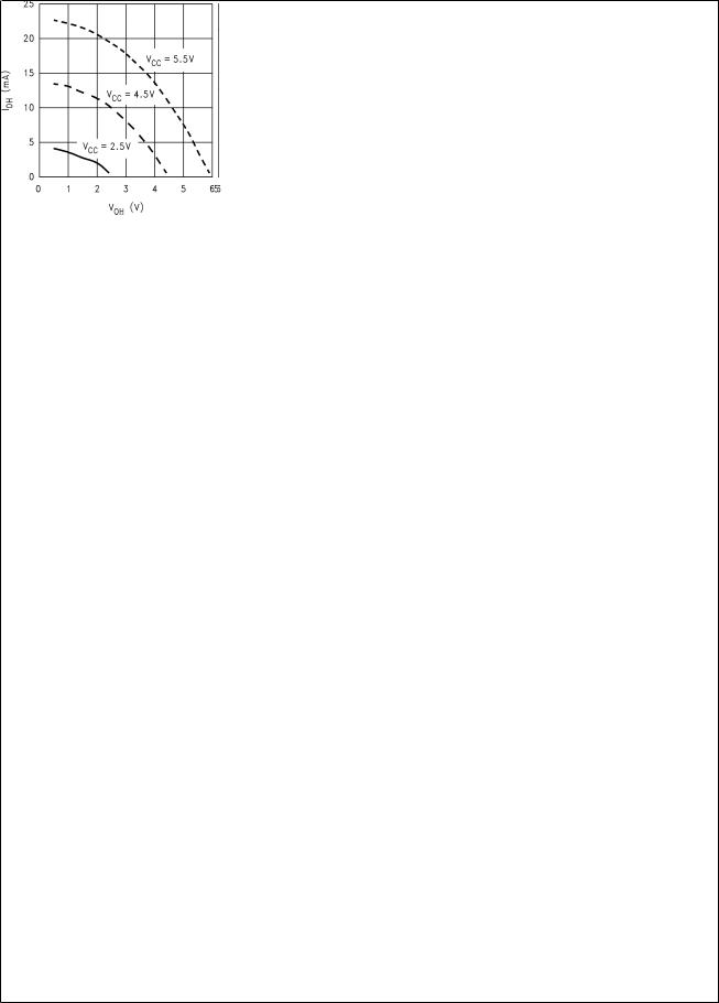
Port L/G Push-Pull Sink Current Port D Source Current
DS012060-20 |
DS012060-21 |
www.national.com |
4 |

Typical Performance Characteristics (Continued)
Port D Sink Current
DS012060-22
AC Electrical Characteristics
COP912C/COP912CH; 0ÊC ≤ TA ≤ +70ÊC unless otherwise specified
Parameter |
|
Conditions |
Min |
Typ |
Max |
Units |
|
|
|
|
|
|
|
INSTRUCTION CYCLE TIME (tc) |
|
|
|
|
|
|
Crystal/Resonator |
4.0V |
≤ VCC ≤ 5.5V |
2 |
|
DC |
µs |
|
2.3V |
≤ VCC < 4.0V |
2.5 |
|
DC |
µs |
R/C Oscillator |
4.0V |
≤ VCC ≤ 5.5V |
3 |
|
DC |
µs |
|
2.3V |
≤ VCC < 4.0V |
7.5 |
|
DC |
µs |
Inputs |
|
|
|
|
|
|
tSetup |
4.0V |
≤ VCC ≤ 5.5V |
200 |
|
|
ns |
|
2.3V |
≤ VCC < 4.0V |
500 |
|
|
ns |
tHold |
4.0V |
≤ VCC ≤ 5.5V |
60 |
|
|
ns |
|
2.3V |
≤ VCC < 4.0V |
150 |
|
|
ns |
Output Propagation Delay |
RL = 2.2 kΩ, CL = 100 pF |
|
|
|
|
|
tPD1, tPD0 |
|
|
|
|
|
|
SO, SK |
4.0V |
≤ VCC ≤ 5.5V |
|
|
0.7 |
µs |
|
2.3V |
≤ VCC < 4.0V |
|
|
1.75 |
µs |
All Others |
4.0V |
≤ VCC ≤ 5.5V |
|
|
1 |
µs |
|
2.3V |
≤ VCC < 4.0V |
|
|
5 |
µs |
Input Pulse Width |
|
|
|
|
|
|
Interrupt Input High Time |
|
|
1 tc |
|
|
|
Interrupt Input Low Time |
|
|
1 tc |
|
|
|
Timer Input High Time |
|
|
1 tc |
|
|
|
Timer Input Low Time |
|
|
1 tc |
|
|
|
|
|
|
|
|
|
|
MICROWIRE Setup Time (tµWS) |
|
|
20 |
|
|
ns |
MICROWIRE Hold Time (tµWH) |
|
|
56 |
|
|
ns |
MICROWIRE Output |
|
|
|
|
220 |
ns |
Propagation Delay (tµPD) |
|
|
|
|
|
|
Reset Pulse Width |
|
|
1.0 |
|
|
µs |
|
|
|
|
|
|
|
COP912C
5 |
www.national.com |

COP912C
COP912C/COP912CH Pinout
20 DIP |
20 SO Wide |
|
DS012060-3
DS012060-4
Top View |
|
Top View |
|
Order Number COP912C-XXX/N, |
|||
Order Number COP912C-XXX/WM, |
|||
COP912CH-XXX/N |
|
||
|
COP912CH-XXX/WM |
||
|
|
||
|
FIGURE 2. COP912C/COP912CH Pinout |
||
Pin Description
VCC and GND are the power supply pins.
CKI is the clock input. This can come from an external source, a R/C generated oscillator or a crystal (in conjunction with CKO). See Oscillator description.
RESET is the master reset input. See Reset description.
PORT L is an 8-bit I/O port.
There are two registers associated to configure the L port: a data register and a configuration register. Therefore, each L I/O bit can be individually configured under software control as shown below:
Port L |
Port L |
PORT L |
Config. |
Data |
Setup |
|
|
|
0 |
0 |
Hi-Z Input (TRI-STATE) |
|
|
|
0 |
1 |
Input with Weak Pull-Up |
|
|
|
1 |
0 |
Push-Pull Zero Output |
|
|
|
1 |
1 |
Push-Pull One Output |
|
|
|
Three data memory address locations are allocated for this port, one each for data register [00D0], configuration register [00D1] and the input pins [00D2].
PORT G is an 8-bit port with 6 I/O pins (G0±G5) and 2 input pins (G6, G7).
All eight G-pins have Schmitt Triggers on the inputs.
There are two registers associated to configure the G port: a data register and a configuration register. Therefore each G port bit can be individually configured under software control as shown below:
Port G |
Port G |
PORT G |
Config. |
Data |
Setup |
|
|
|
0 |
0 |
Hi-Z Input (TRI-STATE) |
|
|
|
0 |
1 |
Input with Weak Pull-Up |
|
|
|
1 |
0 |
Push-Pull Zero Output |
|
|
|
1 |
1 |
Push-Pull One Output |
|
|
|
Three data memory address locations are allocated for this port, one for data register [00D4], one for configuration register [00D5] and one for the input pins [00D6]. Since G6 and
G7 are Hi-Z input only pins, any attempt by the user to configure them as outputs by writing a one to the configuration register will be disregarded. Reading the G6 and G7 configuration bits will return zeroes. Note that the chip will be placed in the Halt mode by writing a ª1º to the G7 data bit.
Six pins of Port G have alternate features:
G0 INTR (an external interrupt)
G3 TIO (timer/counter input/output)
G4 SO (MICROWIRE serial data output)
G5 SK (MICROWIRE clock I/O)
G6 SI (MICROWIRE serial data input)
G7 CKO crystal oscillator output (selected by mask option) or HALT restart input/general purpose input (if clock option is R/C- or external clock)
Pins G1 and G2 currently do not have any alternate functions.
The selection of alternate Port G functions are done through registers PSW [00EF] to enable external interrupt and CNTRL [00EE] to select TIO and MICROWIRE operations.
Functional Description
The internal architecture is shown in the block diagram. Data paths are illustrated in simplified form to depict how the various logic elements communicate with each other in implementing the instruction set of the device.
ALU AND CPU REGISTERS
The ALU can do an 8-bit addition, subtraction, logical or shift operations in one cycle time. There are five CPU registers:
A is the 8-bit Accumulator register
PC is the 15-bit Program Counter register
PU is the upper 7 bits of the program counter (PC)
PL is the lower 8 bits of the program counter (PC)
Bis the 8-bit address register and can be auto incremented or decremented
Xis the 8-bit alternate address register and can be auto incremented or decremented.
www.national.com |
6 |
 Loading...