


NSC DS8923AN, DS8923AM, DS8922N, DS8922M, DS8922AN Datasheet
...June 1998
DS8922/DS8922A/DS8923A TRI-STATE®
RS-422 Dual Differential Line Driver and Receiver Pairs
General Description
The DS8922/22A and DS8923A are Dual Differential Line Driver and Receiver pairs. These devices are designed specifically for applications meeting the ST506, ST412 and ESDI Disk Drive Standards. In addition, the devices meet the requirements of the EIA Standard RS-422.
These devices offer an input sensitivity of 200 mV over a
±7V common mode operating range. Hysteresis is incorporated (typically 70 mV) to improve noise margin for slowly changing input waveforms. An input fail-safe circuit is provided such that if the receiver inputs are open the output assumes the logical one state.
The DS8922A and DS8923A drivers are designed to provide unipolar differential drive to twisted pair or parallel wire transmission lines. Complementary outputs are logically ANDed and provide an output skew of 0.5 ns (typ.) with propagation delays of 12 ns.
Both devices feature TRI-STATE outputs. The DS8922/22A have independent control functions common to a driver and receiver pair. The DS8923A has separate driver and receiver control functions.
Power up/down circuitry is featured which will TRI-STATE the outputs and prevent erroneous glitches on the transmission lines during system power up or power down operation.
The DS8922/22A and DS8923A are designed to be compatible with TTL and CMOS.
Features
n 12 ns typical propagation delay n Output skew Ð ±0.5 ns typical
nMeets the requirements of EIA Standard RS-422
nComplementary Driver Outputs
nHigh differential or common-mode input voltage ranges of ±7V
n±0.2V receiver sensitivity over the input voltage range
nReceiver input fail-safe circuitry
nReceiver input hysteresis Ð 70 mV typical
nGlitch free power up/down
nTRI-STATE outputs
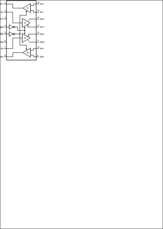
Connection Diagrams
DS8922A Dual-In-Line
DS008511-1
Order Number DS8922M, DS8922N,
DS8922AM or DS8922AN
See NS Package Number M16A or N16E
TRI-STATE® is a registered trademark of National Semiconductor Corp.
Pairs Receiver and Driver Line Differential Dual 422-RS STATE-TRI DS8922/DS8922A/DS8923A
© 1998 National Semiconductor Corporation |
DS008511 |
www.national.com |
Connection Diagrams (Continued)
DS8923A Dual-In-Line
|
|
|
|
|
|
|
|
|
|
|
|
|
|
DS008511-2 |
||
|
|
|
|
|
|
|
|
|
|
|
Order Number DS8923AM, DS8923AN, |
|||||
|
|
|
|
|
|
|
|
|
|
|
See NS Package Number M16A or N16E |
|||||
Truth Tables |
|
|
|
|
|
|
|
|||||||||
DS8922/22A |
|
|
|
|
|
|
|
|||||||||
|
|
|
|
|
|
|
|
|
|
|
|
|
|
|
|
|
|
|
EN1 |
|
|
|
|
EN2 |
|
|
RO1 |
RO2 |
DO1 |
|
DO2 |
||
0 |
|
|
0 |
|
|
ACTIVE |
ACTIVE |
ACTIVE |
|
ACTIVE |
||||||
|
|
|
|
|
|
|
|
|
|
|
|
|
|
|
|
|
1 |
|
|
0 |
|
|
HI-Z |
ACTIVE |
HI-Z |
|
ACTIVE |
||||||
|
|
|
|
|
|
|
|
|
|
|
|
|
|
|
|
|
0 |
|
|
1 |
|
|
ACTIVE |
HI-Z |
ACTIVE |
|
HI-Z |
||||||
|
|
|
|
|
|
|
|
|
|
|
|
|
|
|
|
|
1 |
|
|
1 |
|
|
HI-Z |
HI-Z |
HI-Z |
|
HI-Z |
||||||
|
|
|
|
|
|
|
|
|
|
|
|
|
|
|
|
|
DS8923A |
|
|
|
|
|
|
|
|||||||||
|
|
|
|
|
|
|
|
|
|
|
|
|
||||
|
DEN |
|
|
REN |
|
RO1 |
RO2 |
|
DO1 |
|
DO2 |
|
||||
0 |
|
|
0 |
|
|
ACTIVE |
ACTIVE |
|
ACTIVE |
|
ACTIVE |
|
||||
|
|
|
|
|
|
|
|
|
|
|
|
|
|
|
||
1 |
|
|
0 |
|
|
ACTIVE |
ACTIVE |
|
HI-Z |
|
HI-Z |
|
||||
|
|
|
|
|
|
|
|
|
|
|
|
|
|
|
||
0 |
|
|
1 |
|
|
HI-Z |
HI-Z |
|
ACTIVE |
|
ACTIVE |
|
||||
|
|
|
|
|
|
|
|
|
|
|
|
|
|
|
||
1 |
|
|
1 |
|
|
HI-Z |
HI-Z |
|
HI-Z |
|
HI-Z |
|
||||
|
|
|
|
|
|
|
|
|
|
|
|
|
|
|
|
|
www.national.com |
2 |

Absolute Maximum Ratings (Note 1)
If Military/Aerospace specified devices are required, please contact the National Semiconductor Sales Office/ Distributors for availability and specifications.
Supply Voltage |
7V |
Drive Input Voltage |
−0.5V to +7V |
Output Voltage |
5.5V |
Receiver Output Sink Current |
50 mA |
Receiver Input Voltage |
±10V |
Differential Input Voltage |
±12V |
Maximum Package Power Dissipation @ +25ÊC |
|
M Package |
1300 mW |
N Package |
1450 mW |
Derate M Package 10.4 mW/ÊC above +25ÊC |
|
Derate N Package 11.6 mW/ÊC above +25ÊC |
|
Storage Temperature Range |
−65ÊC to +165ÊC |
Lead Temp. (Soldering, 4 seconds) |
260ÊC |
Recommended Operating
Conditions
|
Min |
Max |
Units |
Supply Voltage |
4.5 |
5.5 |
V |
Temperature (TA) |
0 |
70 |
ÊC |
DS8922/22A and DS8923A Electrical Characteristics(Notes 2, 3, 4)
Symbol |
Conditions |
Min |
Typ |
Max |
Units |
|||||||
|
|
|
|
|
|
|
|
|
|
|
|
|
RECEIVER |
|
|
|
|
|
|
|
|||||
|
|
|
|
|
|
|
|
|
|
|
|
|
VTH |
−7V ≤ VCM ≤ +7V |
|
−200 |
±35 |
+200 |
mV |
||||||
VHYST |
−7V ≤ VCM ≤ +7V |
|
15 |
70 |
|
mV |
||||||
RIN |
V IN = −7V, +7V (Other Input = GND) |
4.0 |
6.0 |
|
kΩ |
|||||||
IIN |
VIN = 10V |
|
|
|
3.25 |
mA |
||||||
|
|
|
|
|
|
VIN = −10V |
|
|
|
−3.25 |
mA |
|
VOH |
V CC = MIN, IOH = − 400 µA |
|
2.5 |
|
|
V |
||||||
VOL |
V CC = MAX, IOL = 8 mA |
|
|
|
0.5 |
V |
||||||
ISC |
V CC = MAX, VOUT = 0V |
|
−15 |
|
−100 |
mA |
||||||
DRIVER |
|
|
|
|
|
|
|
|||||
|
|
|
|
|
|
|
|
|
|
|
|
|
VOH |
V CC = MIN, IOH = −20 mA |
|
2.5 |
|
|
V |
||||||
VOL |
V CC = MIN, IOL = +20 mA |
|
|
|
0.5 |
V |
||||||
IOFF |
V CC = 0V, VOUT = 5.5V |
|
|
|
100 |
µA |
||||||
|
|
|
|
|
|
|
|
|
|
|
||
|VT|±| |
|
VT |
| |
|
|
|
|
|
0.4 |
V |
||
VT |
|
|
|
2.0 |
|
|
V |
|||||
|
|
|
|
|
|
|
|
|
|
|
|
|
|
|
|
|
|
|
|
|
|
||||
|VOS± |
V |
|
| |
|
|
|
|
|
0.4 |
V |
||
OS |
|
|
|
|
|
|||||||
ISC |
V CC = MAX, VOUT = 0V |
|
−30 |
|
−150 |
mA |
||||||
DRIVER and RECEIVER |
|
|
|
|
|
|||||||
|
|
|
|
|
|
|
|
|
|
|
|
|
IOZ |
|
|
VOUT = 2.5V |
|
|
50 |
µA |
|||||
TRI-STATE |
VCC = MAX |
|
VOUT = 0.4V |
|
|
−50 |
µA |
|||||
Leakage |
|
|
|
|
|
|
|
|||||
|
|
|
|
|
|
|
|
|
|
|
|
|
ICC |
VCC = MAX |
|
ACTIVE |
|
|
76 |
mA |
|||||
|
|
|
|
|
|
|
|
TRI-STATE |
|
|
78 |
mA |
|
|
|
|
|
|
|
|
|
|
|
|
|
DRIVER and ENABLE INPUTS |
|
|
|
|
|
|||||||
|
|
|
|
|
|
|
|
|
|
|
|
|
VIH |
|
|
|
2.0 |
|
|
V |
|||||
VIL |
|
|
|
|
|
0.8 |
V |
|||||
IIL |
V CC = MAX, VIN = 0.4V |
|
|
−40 |
−200 |
µA |
||||||
IIH |
V CC = MAX, VIN = 2.7V |
|
|
|
20 |
µA |
||||||
II |
V CC = MAX, VIN = 7.0V |
|
|
|
100 |
µA |
||||||
VCL |
V CC = MIN, IIN = −18 mA |
|
|
|
−1.5 |
V |
||||||
3 |
www.national.com |

Receiver Switching Characteristics
(Figures 1, 2, 3)
Parameter |
Conditions |
Min |
Typ |
Max |
|
Units |
|
|
|
|
|
|
|
|
|
|
|
|
|
8922 |
|
8922A/23A |
|
|
|
|
|
|
|
|
|
TpLH |
CL = 30 pF |
|
12 |
22.5 |
|
20 |
ns |
TpHL |
CL = 30 pF |
|
12 |
22.5 |
|
20 |
ns |
|TpLH±T pHL| |
CL = 30 pF |
|
0.5 |
5 |
|
3.5 |
ns |
Skew (Channel to Channel) |
CL = 30 pF |
|
0.5 |
3.0 |
|
2.0 |
ns |
|
|
|
|
|
|
|
|
TpLZ |
CL = 15 pF S2 Open |
|
15 |
|
|
|
ns |
TpHZ |
CL = 15 pF S1 Open |
|
15 |
|
|
|
ns |
TpZL |
CL = 30 pF S2 Open |
|
20 |
|
|
|
ns |
TpZH |
CL = 30 pF S1 Open |
|
20 |
|
|
|
ns |
Driver Switching Characteristics
Parameter |
Conditions |
|
Min |
|
Typ |
|
Max |
Units |
|
|
|
|
|
|
|
|
|
|
|
|
|
|
|
|
|
8922 |
|
8922A/23A |
|
|
|
|
|
|
|
|
|
|
|
SINGLE ENDED CHARACTERISTICS (Figures 4, 5, 6, 8) |
|
|
|
|
|
|
|
||
|
|
|
|
|
|
|
|
|
|
TpLH |
CL = 30 pF |
|
|
|
12 |
15 |
|
15 |
ns |
TpHL |
CL = 30 pF |
|
|
|
12 |
15 |
|
15 |
ns |
TTLH |
CL = 30 pF |
|
|
|
5 |
10 |
|
10 |
ns |
TTHL |
CL = 30 pF |
|
|
|
5 |
10 |
|
10 |
ns |
|TpLH±T pHL| |
CL = 30 pF |
|
|
|
0.5 |
|
|
|
ns |
Skew |
CL = 30 pF (Note 5) |
|
|
|
0.5 |
5 |
|
3.5 |
ns |
|
|
|
|
|
|
|
|
|
|
Skew (Channel to Channel) |
|
|
|
|
0.5 |
3.0 |
|
2.0 |
ns |
|
|
|
|
|
|
|
|
|
|
TpLZ |
CL = 30 pF |
|
|
|
15 |
|
|
|
ns |
TpHZ |
CL = 30 pF |
|
|
|
15 |
|
|
|
ns |
TpZL |
CL = 30 pF |
|
|
|
20 |
|
|
|
ns |
TpZH |
CL = 30 pF |
|
|
|
20 |
|
|
|
ns |
DIFFERENTIAL SWITCHING CHARACTERISTICS (Note 6), (Figure 4) |
|
|
|
|
|
||||
|
|
|
|
|
|
|
|
|
|
TpLH |
CL = 30 pF |
|
|
|
12 |
15 |
|
15 |
ns |
TpHL |
CL = 30 pF |
|
|
|
12 |
15 |
|
15 |
ns |
|TpLH±T pHL| |
CL = 30 pF |
|
|
|
0.5 |
6.0 |
|
2.75 |
ns |
Note 1: ªAbsolute Maximum Ratingsº are those values beyond which the safety of the device cannot be guaranteed. They are not meant to imply that the device should be operated at these limits. The Table of ªElectrical Characteristicsº provides conditions for actual device operation.
Note 2: All currents into device pins are shown as positive values; all currents out of the device are shown as negative; all voltages are referenced to ground unless otherwise specified. All values shown as max or min are classified on absolute value basis.
Note 3: All typical values are VCC = 5V, TA = 25ÊC.
Note 4: Only one output at a time should be shorted.
Note 5: Difference between complementary outputs at the 50% point.
Note 6: Differential Delays are defined as calculated results from single ended rise and fall time measurements. This approach in establishing AC performance specifications has been taken due to limitations of available Automatic Test Equipment (ATE).
The calculated ATE results assume a linear transition between measurement points and are a result of the following equations:
Where:
Tcp = Crossing Point
Tra, Trb, Tfa and Tfb are time measurements with respect to the input.
www.national.com |
4 |

Switching Time Waveforms
DS008511-3
AC Test Circuits and Switching Waveforms
DS008511-4
FIGURE 1.
DS008511-5
FIGURE 2.
5 |
www.national.com |
 Loading...