


NSC COPCFH988V, COPCFH988N, COPCFH984N, COPCF988V, COPCF988N Datasheet
...September 1999
COP888CF
8-Bit CMOS ROM Based Microcontrollers with 4k
Memory and A/D Converter
General Description
The COP888CF ROM based microcontrollers are highly integrated COP8™ Feature core devices with 4k memory and advanced features including an A/D Converter. These singlechip CMOS devices are suited for applications requiring a full featured controller with an 8-bit A/D converter. Pin and software compatible (different VCC range) 16k/32k OTP (One Time Programmable) versions are available (COP87L88CF Family) for pre-production, and for use with a range of COP8 software and hardware development tools.
Family features include an 8-bit memory mapped architecture, 10 MHz CKI with 1 µs instruction cycle, two multifunction 16-bit timer/counters, MICROWIRE/PLUS™ serial I/O, one 8-bit/8-channel A/D converter with prescaler and both differential and single ended modes, crystal or R/C oscillator, two power saving HALT/IDLE modes, idle timer, MIWU, high current outputs, software selectable I/O options, WATCHDOG™ timer and Clock Monitor, 2.5V to 6.0V operation and 28/40/44 pin packages.
Devices included in this datasheet are:
Device |
Memory |
RAM |
I/O Pins |
|
Packages |
Temperature |
|
|
|
|
|
|
|
COP884CF |
4k bytes ROM |
128 bytes |
22 |
28 |
DIP/SOIC |
-40 to +85ÊC |
COP984CF |
4k bytes ROM |
128 bytes |
22 |
28 |
DIP/SOIC |
-0 to +70ÊC |
COP888CF |
4k bytes ROM |
128 bytes |
34/38 |
40 |
DIP, 44 PLCC |
-40 to +85ÊC |
COP988CF |
4k bytes ROM |
128 bytes |
34/38 |
40 |
DIP, 44 PLCC |
-0 to +70ÊC |
|
|
|
|
|
|
|
Key Features
nA/D converter (8-bit, 8-channel, with prescaler and both differential and single ended modes)
nTwo 16-bit timers, each with two 16-bit registers supporting:
ÐProcessor Independent PWM mode
ÐExternal Event counter mode
ÐInput Capture mode
n4 kbytes of on-chip ROM
n128 bytes of on-chip RAM
Additional Peripheral Features
nIdle Timer
nMulti-Input Wake Up (MIWU) with optional interrupts (8)
nWATCHDOG and Clock Monitor logic
nMICROWIRE/PLUS serial I/O
n Schmitt trigger inputs on Port G
CPU/Instruction Set Feature
n1 µs instruction cycle time
nTen multi-source vectored interrupts servicing
ÐExternal interrupt with selectable edge
ÐIdle Timer T0
ÐTwo Timers (Each with 2 interrupts)
ÐMICROWIRE/PLUS
ÐMulti-Input Wake Up
ÐSoftware Trap
ÐDefault VIS (default interrupt)
nVersatile and easy to use instruction set
n8-bit Stack Pointer (SP) Ð stack in RAM
nTwo 8-bit Register Indirect Data Memory Pointers (B, X)
Fully Static CMOS
I/O Features
nMemory mapped I/O
nSoftware selectable I/O options (TRI-STATE® Output, Push-Pull Output, Weak Pull-Up Input, High Impedance Input)
nHigh current outputs
nPackages:
Ð44 PLCC with 38 I/O pins
Ð40 DIP with 34 I/O pins
Ð28 DIP/SO with 22 I/O pins
nLow current drain (typically < 1 µA)
nSingle supply operation: 2.5V to 6.0V
nTemperature ranges: 0ÊC to +70ÊC, and −40ÊC to +85ÊC
Development Support
nEmulation and OTP devices
nReal time emulation and full program debug offered by MetaLink Development System
is a trademark of National Semiconductor Corporation.
is a trademark of National Semiconductor Corporation. MICROWIRE/PLUS™ is a trademark of National Semiconductor Corporation. TRI-STATE® is a registered trademark of National Semiconductor Corporation. WATCHDOG™ is a trademark of National Semiconductor Corporation. iceMASTER™ is a trademark of MetaLink Corporation.
Converter A/D and Memory 4k with Microcontrollers Based ROM CMOS Bit-8 COP888CF
© 1999 National Semiconductor Corporation |
DS009425 |
www.national.com |

Block Diagram
DS009425-1
FIGURE 1. Block Diagram
www.national.com |
2 |
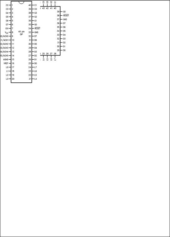
Connection Diagrams
Plastic Chip Carrier
Dual-In-Line Package
DS009425-37
DS009425-2 |
Top View |
|
Top View |
||
Order Number COP884CF-XXX/N, |
||
Order Number COP888CF-XXX/V |
||
COP884CF-XXX/WM, COP984CF-XXX/N, |
||
COP988CF-XXX/V or COP988CFH-XXX/V |
||
COP984CFH-XXX/N, COP984CFH-XXX/WM |
||
See NS Plastic Chip Package Number V44A |
||
or COP984CFH-XXX/WM |
||
|
||
|
See NS Package Number N28B or M28B |
|
Dual-In-Line Package |
||
DS009425-4
Top View
Order Number COP888CF-XXX/N,
COP988CF-XXX/N or COP988CFH-XXX/N
See NS Molded Package Number N40A
FIGURE 2. Connection Diagrams
3 |
www.national.com |

Connection Diagrams (Continued)
Pinouts for 28-, 40and 44-Pin Packages
|
Port |
Type |
Alt. Fun |
Alt. Fun |
28-Pin Pack. |
40-Pin Pack. |
44-Pin Pack. |
|
|
|
|
|
|
|
|
|
|
|
L0 |
I/O |
MIWU |
|
11 |
17 |
Ð |
|
|
L1 |
I/O |
MIWU |
|
12 |
18 |
Ð |
|
|
L2 |
I/O |
MIWU |
|
13 |
19 |
19 |
|
|
L3 |
I/O |
MIWU |
|
14 |
20 |
20 |
|
|
L4 |
I/O |
MIWU |
T2A |
15 |
21 |
25 |
|
|
L5 |
I/O |
MIWU |
T2B |
16 |
22 |
26 |
|
|
L6 |
I/O |
MIWU |
|
17 |
23 |
27 |
|
|
L7 |
I/O |
MIWU |
|
18 |
24 |
28 |
|
|
|
|
|
|
|
|
|
|
|
G0 |
I/O |
INT |
|
25 |
35 |
39 |
|
|
G1 |
WDOUT |
|
|
26 |
36 |
40 |
|
|
G2 |
I/O |
T1B |
|
27 |
37 |
41 |
|
|
G3 |
I/O |
T1A |
|
28 |
38 |
42 |
|
|
G4 |
I/O |
SO |
|
1 |
3 |
3 |
|
|
G5 |
I/O |
SK |
|
2 |
4 |
4 |
|
|
G6 |
I |
SI |
|
3 |
5 |
5 |
|
|
G7 |
I/CKO |
HALT Restart |
|
4 |
6 |
6 |
|
|
|
|
|
|
|
|
|
|
|
I0 |
I |
ACH0 |
|
7 |
9 |
9 |
|
|
I1 |
I |
ACH1 |
|
8 |
10 |
10 |
|
|
I2 |
I |
ACH2 |
|
|
11 |
11 |
|
|
I3 |
I |
ACH3 |
|
|
12 |
12 |
|
|
I4 |
I |
ACH4 |
|
|
13 |
13 |
|
|
I5 |
I |
ACH5 |
|
|
14 |
14 |
|
|
I6 |
I |
ACH6 |
|
|
|
15 |
|
|
I7 |
I |
ACH7 |
|
|
|
16 |
|
|
|
|
|
|
|
|
|
|
|
D0 |
O |
|
|
19 |
25 |
29 |
|
|
D1 |
O |
|
|
20 |
26 |
30 |
|
|
D2 |
O |
|
|
21 |
27 |
31 |
|
|
D3 |
O |
|
|
22 |
28 |
32 |
|
|
D4 |
O |
|
|
|
29 |
33 |
|
|
D5 |
O |
|
|
|
30 |
34 |
|
|
D6 |
O |
|
|
|
31 |
35 |
|
|
D7 |
O |
|
|
|
32 |
36 |
|
|
|
|
|
|
|
|
|
|
|
C0 |
I/O |
|
|
|
39 |
43 |
|
|
C1 |
I/O |
|
|
|
40 |
44 |
|
|
C2 |
I/O |
|
|
|
1 |
1 |
|
|
C3 |
I/O |
|
|
|
2 |
2 |
|
|
C4 |
I/O |
|
|
|
|
21 |
|
|
C5 |
I/O |
|
|
|
|
22 |
|
|
C6 |
I/O |
|
|
|
|
23 |
|
|
C7 |
I/O |
|
|
|
|
24 |
|
|
|
|
|
|
|
|
|
|
|
VREF |
+VREF |
|
|
10 |
16 |
18 |
|
|
AGND |
AGND |
|
|
9 |
15 |
17 |
|
|
VCC |
|
|
|
6 |
8 |
8 |
|
|
GND |
|
|
|
23 |
33 |
37 |
|
|
CKI |
|
|
|
5 |
7 |
7 |
|
|
|
|
|
|
24 |
34 |
38 |
|
|
RESET |
|
|
|
|
|||
www.national.com |
4 |

Absolute Maximum Ratings (Note 1)
If Military/Aerospace specified devices are required, please contact the National Semiconductor Sales Office/ Distributors for availability and specifications.
Supply Voltage (VCC) |
7V |
Voltage at Any Pin |
−0.3V to V CC + 0.3V |
Total Current into VCC Pin (Source) |
100 mA |
Total Current out of GND Pin (Sink) |
110 mA |
Storage Temperature Range |
−65ÊC to +140ÊC |
Note 1: Absolute maximum ratings indicate limits beyond which damage to the device may occur. DC and AC electrical specifications are not ensured when operating the device at absolute maximum ratings.
DC Electrical Characteristics 988CF:
0ÊC ≤ TA ≤ +70ÊC unless otherwise specified
|
|
Parameter |
Conditions |
Min |
Typ |
Max |
Units |
|
|
|
|
|
|
|
|
|
Operating Voltage |
|
|
|
|
|
|
|
988CF |
|
2.5 |
|
4.0 |
V |
|
|
998CFH |
|
4.0 |
|
6.0 |
V |
|
|
|
|
|
|
|
|
|
|
Power Supply Ripple (Note 2) |
Peak-to-Peak |
|
|
0.1 VCC |
V |
|
Supply Current (Note 3) |
|
|
|
|
|
||
|
CKI = 10 MHz |
VCC = 6V, tc = 1 µs |
|
|
12.5 |
mA |
|
|
CKI = 4 MHz |
VCC = 6V, tc = 2.5 µs |
|
|
5.5 |
mA |
|
|
CKI = 4 MHz |
VCC = 4V, tc = 2.5 µs |
|
|
2.5 |
mA |
|
|
CKI = 1 MHz |
VCC = 4V, tc = 10 µs |
|
|
1.4 |
mA |
|
|
HALT Current (Note 4) |
VCC = 6V, CKI = 0 MHz |
|
<0.7 |
8 |
µA |
|
|
|
|
VCC = 4.0V, CKI = 0 MHz |
|
<0.3 |
4 |
µA |
|
IDLE Current |
|
|
|
|
|
|
|
CKI = 10 MHz |
VCC = 6V, tc = 1 µs |
|
|
3.5 |
mA |
|
|
CKI = 4 MHz |
VCC = 6V, tc = 2.5 µs |
|
|
2.5 |
mA |
|
|
CKI = 1 MHz |
VCC = 4.0V, tc = 10 µs |
|
|
0.7 |
mA |
|
|
Input Levels |
|
|
|
|
|
|
|
|
|
|
|
|
|
|
|
RESET |
|
|
|
|
|
|
|
Logic High |
|
0.8 VCC |
|
|
V |
|
|
Logic Low |
|
|
|
0.2 VCC |
V |
|
CKI (External and Crystal Osc. Modes) |
|
|
|
|
|
||
|
Logic High |
|
0.7 VCC |
|
|
V |
|
|
Logic Low |
|
|
|
0.2 VCC |
V |
|
All Other Inputs |
|
|
|
|
|
||
|
Logic High |
|
0.7 VCC |
|
|
V |
|
|
Logic Low |
|
|
|
0.2 VCC |
V |
|
Hi-Z Input Leakage |
VCC = 6V |
−1 |
|
+1 |
µA |
||
|
Input Pullup Current |
VCC = 6V, VIN = 0V |
−40 |
|
−250 |
µA |
|
|
G and L Port Input Hysteresis |
|
|
|
0.35 VCC |
V |
|
Output Current Levels |
|
|
|
|
|
||
D Outputs |
|
|
|
|
|
||
|
Source |
VCC = 4V, VOH = 3.3V |
−0.4 |
|
|
mA |
|
|
|
|
VCC = 2.5V, VOH = 1.8V |
−0.2 |
|
|
mA |
|
Sink |
VCC = 4V, VOL = 1V |
10 |
|
|
mA |
|
|
|
|
VCC = 2.5V, VOL = 0.4V |
2.0 |
|
|
mA |
|
All Others |
|
|
|
|
|
|
|
Source (Weak Pull-Up Mode) |
VCC = 4V, VOH = 2.7V |
−10 |
|
−100 |
µA |
|
|
|
|
VCC = 2.5V, VOH = 1.8V |
−2.5 |
|
−33 |
µA |
|
Source (Push-Pull Mode) |
VCC = 4V, VOH = 3.3V |
−0.4 |
|
|
mA |
|
|
|
|
VCC = 2.5V, VOH = 1.8V |
−0.2 |
|
|
mA |
|
Sink (Push-Pull Mode) |
VCC = 4V, VOL = 0.4V |
1.6 |
|
|
mA |
|
|
|
|
VCC = 2.5V, VOL = 0.4V |
0.7 |
|
|
mA |
|
TRI-STATE Leakage |
VCC = 6.0V |
−1 |
|
+1 |
µA |
|
5 |
www.national.com |

DC Electrical Characteristics 988CF: (Continued)
0ÊC ≤ TA ≤ +70ÊC unless otherwise specified
Parameter |
Conditions |
Min |
Typ |
Max |
Units |
Allowable Sink/Source |
|
|
|
|
|
Current per Pin |
|
|
|
|
|
D Outputs (Sink) |
|
|
|
15 |
mA |
All others |
|
|
|
3 |
mA |
|
|
|
|
|
|
Maximum Input Current |
TA = 25ÊC |
|
|
±100 |
mA |
without Latchup (Note 7) |
|
|
|
|
|
|
|
|
|
|
|
RAM Retention Voltage, Vr |
500 ns Rise |
2 |
|
|
V |
|
and Fall Time (Min) |
|
|
|
|
|
|
|
|
|
|
Input Capacitance |
|
|
|
7 |
pF |
|
|
|
|
|
|
Load Capacitance on D2 |
|
|
|
1000 |
pF |
|
|
|
|
|
|
Note 2: Rate of voltage change must be less then 0.5 V/ms.
Note 3: Supply current is measured after running 2000 cycles with a square wave CKI input, CKO open, inputs at rails and outputs open.
Note 4: The HALT mode will stop CKI from oscillating in the RC and the Crystal configurations. Test conditions: All inputs tied to VCC, L and G0±G5 configured as outputs and set high. The D port set to zero. The A/D is disabled. VREF is tied to AGND (effectively shorting the Reference resistor). The clock monitor is disabled.
A/D Converter Specifications
VCC = 5V ±10% (VSS − 0.050V) |
≤ Any Input ≤ (VCC + 0.050V) |
|
|
|
|
|||
Parameter |
|
|
Conditions |
Min |
Typ |
Max |
Units |
|
|
|
|
|
|
|
|
|
|
Resolution |
|
|
|
|
|
|
8 |
Bits |
|
|
|
|
|
|
|
||
Reference Voltage Input |
|
AGND = 0V |
3 |
|
VCC |
V |
||
Absolute Accuracy |
|
VREF = VCC |
|
|
±1 |
LSB |
||
Non-Linearity |
|
VREF = VCC |
|
|
|
|
||
|
|
Deviation from the |
|
|
±1¤2 |
LSB |
||
|
|
Best Straight Line |
|
|
|
|
||
|
|
|
|
|
|
|
|
|
Differential Non-Linearity |
|
VREF |
= |
VCC |
|
|
±1 2 |
LSB |
|
|
|
|
¤ |
||||
Input Reference Resistance |
|
|
|
|
1.6 |
|
4.8 |
kΩ |
|
|
|
|
|
|
|
|
|
Common Mode Input Range (Note 8) |
|
|
|
AGND |
|
VREF |
V |
|
DC Common Mode Error |
|
|
|
|
|
|
±1¤4 |
LSB |
Off Channel Leakage Current |
|
|
|
|
|
1 |
|
µA |
On Channel Leakage Current |
|
|
|
|
|
1 |
|
µA |
|
|
|
|
|
|
|
|
|
A/D Clock Frequency (Note 6) |
|
|
|
|
0.1 |
|
1.67 |
MHz |
|
|
|
|
|
|
|
|
|
Conversion Time (Note 5) |
|
|
|
|
|
12 |
|
A/D Clock |
|
|
|
|
|
|
|
|
Cycles |
Note 5: Conversion Time includes sample and hold time. |
|
|
|
|
|
|
||
Note 6: See Prescaler description. |
|
|
|
|
|
|
|
|
Note 7: Pins G6 and RESET are designed with a high voltage input network for factory testing. These pins allow input voltages greater than VCC and the pins will have sink current to VCC when biased at voltages greater than VCC (the pins do not have source current when biased at a voltage below VCC). The effective resistance to VCC is 750W (typical). These two pins will not latch up. The voltage at the pins must be limited to less than 14V.
Note 8: For VIN(−) ³VIN(+) the digital output code will be 0000 0000. Two on-chip diodes are tied to each analog input. The diodes will forward conduct for analog input voltages below ground or above the VCC supply. Be careful, during testing at low VCC levels (4.5V), as high level analog inputs (5V) can cause this input diode to conduct Ð especially at elevated temperatures, and cause errors for analog inputs near full-scale. The spec allows 50 mV forward bias of either diod e. This means that as long as the analog VIN does not exceed the supply voltage by more than 50 mV, the output code will be correct. To achieve an absolute 0 VDC to 5 VDC input voltage range will therefore require a minimum supply voltage of 4.950 VDC over temperature variations, initial tolerance and loading. The voltage at any analog input should be −0.3V to V CC +0.3V.
www.national.com |
6 |

AC Electrical Characteristics
0ÊC ≤ TA ≤ +70ÊC unless otherwise specified
Parameter |
Conditions |
Min |
Typ |
Max |
Units |
|
|
|
|
|
|
Instruction Cycle Time (tc) |
|
|
|
|
|
Crystal, Resonator |
4V ≤ VCC ≤ 6V |
1 |
|
DC |
µs |
|
2.5V ≤ VCC < 4V |
2.5 |
|
DC |
µs |
R/C Oscillator |
4V ≤ VCC ≤ 6V |
3 |
|
DC |
µs |
|
2.5V ≤ VCC < 4V |
7.5 |
|
DC |
µs |
Inputs |
|
|
|
|
|
tSETUP |
4V ≤ VCC ≤ 6V |
200 |
|
|
ns |
|
2.5V ≤ VCC < 4V |
500 |
|
|
ns |
tHOLD |
4V ≤ VCC ≤ 6V |
60 |
|
|
ns |
|
2.5V ≤ VCC < 4V |
150 |
|
|
ns |
Output Propagation Delay (Note 9) |
RL = 2.2k, CL = 100 pF |
|
|
|
|
tPD1, tPD0 |
|
|
|
|
|
SO, SK |
4V ≤ VCC ≤ 6V |
|
|
0.7 |
µs |
|
2.5V ≤ VCC < 4V |
|
|
1.75 |
µs |
All Others |
4V ≤ VCC ≤ 6V |
|
|
1 |
µs |
|
2.5V ≤ VCC < 4V |
|
|
2.5 |
µs |
MICROWIRE Setup Time (tUWS) |
|
20 |
|
|
ns |
MICROWIRE Hold Time (tUWH) |
|
56 |
|
|
ns |
MICROWIRE Output Propagation Delay (tUPD) |
|
|
|
220 |
ns |
Input Pulse Width |
|
|
|
|
|
Interrupt Input High Time |
|
1 |
|
|
tc |
Interrupt Input Low Time |
|
1 |
|
|
tc |
Timer Input High Time |
|
1 |
|
|
tc |
Timer Input Low Time |
|
1 |
|
|
tc |
Reset Pulse Width |
|
1 |
|
|
µs |
|
|
|
|
|
|
Note 9: The output propagation delay is referenced to the end of the instruction cycle where the output change occurs.
7 |
www.national.com |

Absolute Maximum Ratings (Note 10)
If Military/Aerospace specified devices are required, please contact the National Semiconductor Sales Office/ Distributors for availability and specifications.
Supply Voltage (VCC) |
7V |
Voltage at Any Pin |
−0.3V to V CC + 0.3V |
Total Current into VCC Pin (Source) |
100 mA |
Total Current out of GND Pin (Sink) |
110 mA |
Storage Temperature Range |
−65ÊC to +140ÊC |
Note 10: Absolute maximum ratings indicate limits beyond which damage to the device may occur. DC and AC electrical specifications are not ensured when operating the device at absolute maximum ratings.
DC Electrical Characteristics 888CF:
−40ÊC ≤ TA ≤ +85ÊC unless otherwise specified
|
|
Parameter |
Conditions |
Min |
Typ |
Max |
Units |
|
|
|
|
|
|
|
|
|
Operating Voltage |
|
2.5 |
|
6 |
V |
|
|
|
|
|
|
|
|
|
|
Power Supply Ripple (Note 11) |
Peak-to-Peak |
|
|
0.1 VCC |
V |
|
Supply Current (Note 12) |
|
|
|
|
|
||
|
CKI = 10 MHz |
VCC = 6V, tc = 1 µs |
|
|
12.5 |
mA |
|
|
CKI = 4 MHz |
VCC = 4V, tc = 2.5 µs |
|
|
2.5 |
mA |
|
|
HALT Current (Note 13) |
VCC = 6V, CKI = 0 MHz |
|
<1 |
10 |
µA |
|
IDLE Current |
|
|
|
|
|
||
|
CKI = 10 MHz |
VCC = 6V, tc = 1 µs |
|
|
3.5 |
mA |
|
|
CKI = 1 MHz |
VCC = 4V, tc = 10 µs |
|
|
0.7 |
mA |
|
|
Input Levels |
|
|
|
|
|
|
|
|
|
|
|
|
|
|
|
RESET |
|
|
|
|
|
|
|
Logic High |
|
0.8 VCC |
|
|
V |
|
|
Logic Low |
|
|
|
0.2 VCC |
V |
|
CKI (External and Crystal Osc. Modes) |
|
|
|
|
|
||
|
Logic High |
|
0.7 VCC |
|
|
V |
|
|
Logic Low |
|
|
|
0.2 VCC |
V |
|
All Other Inputs |
|
|
|
|
|
||
|
Logic High |
|
0.7 VCC |
|
|
V |
|
|
Logic Low |
|
|
|
0.2 VCC |
V |
|
Hi-Z Input Leakage |
VCC = 6V |
−2 |
|
+2 |
µA |
||
|
Input Pullup Current |
VCC = 6V, VIN = 0V |
−40 |
|
−250 |
µA |
|
|
G and L Port Input Hysteresis |
|
|
|
0.35 VCC |
V |
|
Output Current Levels |
|
|
|
|
|
||
D Outputs |
|
|
|
|
|
||
|
Source |
VCC = 4V, VOH = 3.3V |
−0.4 |
|
|
mA |
|
|
|
|
VCC = 2.5V, VOH = 1.8V |
−0.2 |
|
|
mA |
|
Sink |
VCC = 4V, VOL = 1V |
10 |
|
|
mA |
|
|
|
|
VCC = 2.5V, VOL = 0.4V |
2.0 |
|
|
mA |
|
All Others |
|
|
|
|
|
|
|
Source (Weak Pull-Up Mode) |
VCC = 4V, VOH = 2.7V |
−10 |
|
−100 |
µA |
|
|
|
|
VCC = 2.5V, VOH = 1.8V |
−2.5 |
|
−33 |
µA |
|
Source (Push-Pull Mode) |
VCC = 4V, VOH = 3.3V |
−0.4 |
|
|
mA |
|
|
|
|
VCC = 2.5V, VOH = 1.8V |
−0.2 |
|
|
mA |
|
Sink (Push-Pull Mode) |
VCC = 4V, VOL = 0.4V |
1.6 |
|
|
mA |
|
|
|
|
VCC = 2.5V, VOL = 0.4V |
0.7 |
|
|
mA |
|
TRI-STATE Leakage |
VCC = 6.0V |
−2 |
|
+2 |
µA |
|
|
Allowable Sink/Source |
|
|
|
|
|
|
|
Current per Pin |
|
|
|
|
|
|
|
D Outputs (Sink) |
|
|
|
15 |
mA |
|
|
All others |
|
|
|
3 |
mA |
|
|
|
|
|
|
|
|
|
|
Maximum Input Current |
TA = 25ÊC |
|
|
±100 |
mA |
|
|
without Latchup (Note 17) |
|
|
|
|
|
|
|
|
|
|
|
|
|
|
www.national.com |
8 |

DC Electrical Characteristics 888CF: (Continued)
−40ÊC ≤ TA ≤ +85ÊC unless otherwise specified
Parameter |
Conditions |
Min |
Typ |
Max |
Units |
RAM Retention Voltage, Vr |
500 ns Rise |
2 |
|
|
V |
|
and Fall Time (Min) |
|
|
|
|
|
|
|
|
|
|
Input Capacitance |
|
|
|
7 |
pF |
|
|
|
|
|
|
Load Capacitance on D2 |
|
|
|
1000 |
pF |
|
|
|
|
|
|
Note 11: Rate of voltage change must be less then 0.5 V/ms.
Note 12: Supply current is measured after running 2000 cycles with a square wave CKI input, CKO open, inputs at rails and outputs open.
Note 13: The HALT mode will stop CKI from oscillating in the RC and the Crystal configurations. Test conditions: All inputs tied to VCC, L and G0±G5 configured as outputs and set high. The D port set to zero. The A/D is disabled. VREF is tied to AGND (effectively shorting the Reference resistor). The clock monitor is disabled.
9 |
www.national.com |

AC Electrical Characteristics 888CF:
−40ÊC ≤ TA ≤ +85ÊC unless otherwise specified
Parameter |
Conditions |
Min |
Typ |
Max |
Units |
|
|
|
|
|
|
Instruction Cycle Time (tc) |
|
|
|
|
|
Crystal, Resonator |
4V ≤ VCC ≤ 6V |
1 |
|
DC |
µs |
|
2.5V ≤ VCC < 4V |
2.5 |
|
DC |
µs |
R/C Oscillator |
4V ≤ VCC ≤ 6V |
3 |
|
DC |
µs |
|
2.5V ≤ VCC < 4V |
7.5 |
|
DC |
µs |
Inputs |
|
|
|
|
|
tSETUP |
4V ≤ VCC ≤ 6V |
200 |
|
|
ns |
|
2.5V ≤ VCC < 4V |
500 |
|
|
ns |
tHOLD |
4V ≤ VCC ≤ 6V |
60 |
|
|
ns |
|
2.5V ≤ VCC < 4V |
150 |
|
|
ns |
Output Propagation Delay (Note 14) |
RL = 2.2k, CL = 100 pF |
|
|
|
|
tPD1, tPD0 |
|
|
|
|
|
SO, SK |
4V ≤ VCC ≤ 6V |
|
|
0.7 |
µs |
|
2.5V ≤ VCC < 4V |
|
|
1.75 |
µs |
All Others |
4V ≤ VCC ≤ 6V |
|
|
1 |
µs |
|
2.5V ≤ VCC < 4V |
|
|
2.5 |
µs |
MICROWIRE Setup Time (tUWS) |
|
20 |
|
|
ns |
MICROWIRE Hold Time (tUWH) |
|
56 |
|
|
ns |
MICROWIRE Output Propagation Delay (tUPD) |
|
|
|
220 |
ns |
Input Pulse Width |
|
|
|
|
|
Interrupt Input High Time |
|
1 |
|
|
tc |
Interrupt Input Low Time |
|
1 |
|
|
tc |
Timer Input High Time |
|
1 |
|
|
tc |
Timer Input Low Time |
|
1 |
|
|
tc |
Reset Pulse Width |
|
1 |
|
|
µs |
|
|
|
|
|
|
Note 14: The output propagation delay is referenced to end of the instruction cycle where the output change occurs.
A/D Converter Specifications
VCC = 5V ±10% (VSS − 0.050V) |
≤ Any Input ≤ (VCC + 0.050V) |
|
|
|
|
|||
Parameter |
|
|
Conditions |
Min |
Typ |
Max |
Units |
|
|
|
|
|
|
|
|
|
|
Resolution |
|
|
|
|
|
|
8 |
Bits |
|
|
|
|
|
|
|
||
Reference Voltage Input |
|
AGND = 0V |
3 |
|
VCC |
V |
||
Absolute Accuracy |
|
VREF = VCC |
|
|
±1 |
LSB |
||
Non-Linearity |
|
VREF = VCC |
|
|
|
|
||
|
|
Deviation from the |
|
|
±1¤2 |
LSB |
||
|
|
Best Straight Line |
|
|
|
|
||
|
|
|
|
|
|
|
|
|
Differential Non-Linearity |
|
VREF |
= |
VCC |
|
|
±1 2 |
LSB |
|
|
|
|
¤ |
||||
Input Reference Resistance |
|
|
|
|
1.6 |
|
4.8 |
kΩ |
|
|
|
|
|
|
|
|
|
Common Mode Input Range (Note 18) |
|
|
|
AGND |
|
VREF |
V |
|
DC Common Mode Error |
|
|
|
|
|
|
±1¤4 |
LSB |
Off Channel Leakage Current |
|
|
|
|
|
1 |
|
µA |
On Channel Leakage Current |
|
|
|
|
|
1 |
|
µA |
|
|
|
|
|
|
|
|
|
A/D Clock Frequency (Note 16) |
|
|
|
|
0.1 |
|
1.67 |
MHz |
|
|
|
|
|
|
|
|
|
Conversion Time (Note 15) |
|
|
|
|
|
12 |
|
A/D Clock |
|
|
|
|
|
|
|
|
Cycles |
Note 15: Conversion Time includes sample and hold time. |
|
|
|
|
|
|
||
Note 16: See Prescaler description. |
|
|
|
|
|
|
|
|
www.national.com |
10 |
A/D Converter Specifications (Continued)
Note 17: Pins G6 and RESET are designed with a high voltage input network for factory testing. These pins allow input voltages greater than VCC and the pins will have sink current to VCC when biased at voltages greater than VCC (the pins do not have source current when biased at a voltage below VCC). The effective resistance to VCC is 750W (typical). These two pins will not latch up. The voltage at the pins must be limited to less than 14V.
Note 18: For VIN(−) ³VIN(+) the digital output code will be 0000 0000. Two on-chip diodes are tied to each analog input. The diodes will forward conduct for analog input voltages below ground or above the VCC supply. Be careful, during testing at low VCC levels (4.5V), as high level analog inputs (5V) can cause this input diode to conduct Ð especially at elevated temperatures, and cause errors for analog inputs near full-scale. The spec allows 50 mV forward bias of either diod e. This means that as long as the analog VIN does not exceed the supply voltage by more than 50 mV, the output code will be correct. To achieve an absolute 0 VDC to 5 VDC input voltage range will therefore require a minimum supply voltage of 4.950 VDC over temperature variations, initial tolerance and loading. The voltage on any analog input should be −0.3V to V CC +0.3V.
DS009425-26
FIGURE 3. MICROWIRE/PLUS Timing
11 |
www.national.com |
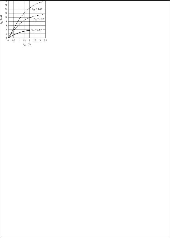
Typical Performance Characteristics (−40ÊC to +85ÊC)
Halt Ð IDDvs VCC |
Idle Ð IDD |
|
(Crystal Clock Option) |
|
DS009425-29 |
|
DS009425-30 |
Dynamic Ð IDD |
Port L/C/G Weak Pull-Up |
(Crystal Clock Option) |
Source Current |
DS009425-31 DS009425-32
Port L/C/G Push-Pull |
Port L/C/G Push-Pull Sink Current |
Source Current |
|
DS009425-34
DS009425-33
www.national.com |
12 |
Typical Performance Characteristics (−40ÊC to +85ÊC) (Continued)
Port D Source Current |
Port D Sink Current |
DS009425-35
Pin Descriptions
VCC and GND are the power supply pins.
VREF and AGND are the reference voltage pins for the on-board A/D converter.
CKI is the clock input. This can come from an R/C generated oscillator, or a crystal oscillator (in conjunction with CKO). See Oscillator Description section.
RESET is the master reset input. See Reset Description section.
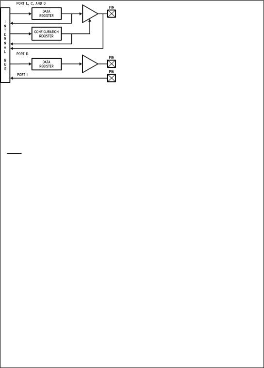
The device contains three bidirectional 8-bit I/O ports (C, G and L), where each individual bit may be independently configured as an input (Schmitt trigger inputs on ports G and L), output or TRI-STATE under program control. Three data memory address locations are allocated for each of these I/O ports. Each I/O port has two associated 8-bit memory mapped registers, the CONFIGURATION register and the output DATA register. A memory mapped address is also reserved for the input pins of each I/O port. (See the memory map for the various addresses associated with the I/O ports.) Figure 4 shows the I/O port configurations. The DATA and CONFIGURATION registers allow for each port bit to be individually configured under software control as shown below:
CONFIGURA- |
DATA |
Port Set-Up |
TION |
|
|
|
|
|
Register |
Register |
|
|
|
|
0 |
0 |
Hi-Z Input |
|
|
(TRI-STATE Output) |
0 |
1 |
Input with Weak Pull-Up |
1 |
0 |
Push-Pull Zero Output |
1 |
1 |
Push-Pull One Output |
|
|
|
DS009425-36
DS009425-6
FIGURE 4. I/O Port Configurations
PORT L is an 8-bit I/O port. All L-pins have Schmitt triggers on the inputs.
Port L supports Multi-Input Wakeup (MIWU) on all eight pins. L4 and L5 are used for the timer input functions T2A and T2B. L0 and L1 are not available on the 44-pin version of the device, since they are replaced by VREF and AGND. L0 and L1 are not terminated on the 44-pin version. Consequently, reading L0 or L1 as inputs will return unreliable data with the 44-pin package, so this data should be masked out with user software when the L port is read for input data. It is recommended that the pins be configured as outputs.
Port L has the following alternate features:
L7 MIWU
L6 MIWU
L5 MIWU or T2B
L4 MIWU or T2A
L3 MIWU
L2 MIWU
L1 MIWU
L0 MIWU
13 |
www.national.com |

Pin Descriptions (Continued)
Port G is an 8-bit port with 5 I/O pins (G0, G2±G5), an input pin (G6), and two dedicated output pins (G1 and G7). Pins G0 and G2±G6 all have Schmitt Triggers on their inputs. Pin G1 serves as the dedicated WDOUT WatchDog output, while pin G7 is either input or output depending on the oscillator mask option selected. With the crystal oscillator option selected, G7 serves as the dedicated output pin for the CKO clock output. With the single-pin R/C oscillator mask option selected, G7 serves as a general purpose input pin, but is also used to bring the device out of HALT mode with a low to high transition on G7. There are two registers associated with the G Port, a data register and a configuration register. Therefore, each of the 5 I/O bits (G0, G2±G5) can be individually configured under software control.
Since G6 is an input only pin and G7 is the dedicated CKO clock output pin or general purpose input (R/C clock configuration), the associated bits in the data and configuration registers for G6 and G7 are used for special purpose functions as outlined below. Reading the G6 and G7 data bits will return zeros.
Note that the chip will be placed in the HALT mode by writing a ª1º to bit 7 of the Port G Data Register. Similarly the chip will be placed in the IDLE mode by writing a ª1º to bit 6 of the Port G Data Register.
Writing a ª1º to bit 6 of the Port G Configuration Register enables the MICROWIRE/PLUS to operate with the alternate phase of the SK clock. The G7 configuration bit, if set high, enables the clock start up delay after HALT when the R/C clock configuration is used.
|
Config Reg. |
Data Reg. |
|
|
|
G7 |
CLKDLY |
HALT |
|
|
|
G6 |
Alternate SK |
IDLE |
|
|
|
Port G has the following alternate features:
G6 SI (MICROWIRE™ Serial Data Input)
G5 SK (MICROWIRE Serial Clock)
G4 SO (MICROWIRE Serial Data Output)
G3 T1A (Timer T1 I/O)
G2 T1B (Timer T1 Capture Input)
G0 INTR (External Interrupt Input)
Port G has the following dedicated functions:
G7 CKO Oscillator dedicated output or general purpose input
G1 WDOUT WATCHDOG and/or Clock Monitor dedicated output.
Port C is an 8-bit I/O port. The 40-pin device does not have a full complement of Port C pins. The unavailable pins are not terminated. A read operation for these unterminated pins will return unpredictable values.
Port I is an 8-bit Hi-Z input port, and also provides the analog inputs to the A/D converter. The 28-pin device does not have a full complement of Port I pins. The unavailable pins are not terminated (i.e. they are floating). A read operation from these unterminated pins will return unpredictable values. The user should ensure that the software takes this into account by either masking out these inputs, or else restricting the accesses to bit operations only. If unterminated, Port I pins will draw power only when addressed.
Port D is an 8-bit output port that is preset high when RESET goes low. The user can tie two or more D port outputs (except D2) together in order to get a higher drive.
Note: Care must be exercised with the D2 pin operation. At RESET, the external loads on this pin must ensure that the output voltages stay above 0.8 VCC to prevent the chip from entering special modes. Also keep the external loading on D2 to less than 1000 pF.
Functional Description
The architecture of the device is modified Harvard architecture. With the Harvard architecture, the control store program memory (ROM) is separated from the data store memory (RAM). Both ROM and RAM have their own separate addressing space with separate address buses. The architecture, though based on Harvard architecture, permits transfer of data from ROM to RAM.
CPU REGISTERS
The CPU can do an 8-bit addition, subtraction, logical or shift operation in one instruction (tc) cycle time.
There are five CPU registers:
A is the 8-bit Accumulator Register
PC is the 15-bit Program Counter Register
PU is the upper 7 bits of the program counter (PC)
PL is the lower 8 bits of the program counter (PC)
B is an 8-bit RAM address pointer, which can be optionally post auto incremented or decremented.
X is an 8-bit alternate RAM address pointer, which can be optionally post auto incremented or decremented.
SP is the 8-bit stack pointer, which points to the subroutine/ interrupt stack (in RAM). The SP is initialized to RAM address 06F with reset.
All the CPU registers are memory mapped with the exception of the Accumulator (A) and the Program Counter (PC).
PROGRAM MEMORY
Program memory consists of 4096 bytes of ROM. These bytes may hold program instructions or constant data (data tables for the LAID instruction, jump vectors for the JID instruction, and interrupt vectors for the VIS instruction). The program memory is addressed by the 15-bit program counter (PC). All interrupts vector to program memory location 0FF Hex.
DATA MEMORY
The data memory address space includes the on-chip RAM and data registers, the I/O registers (Configuration, Data and Pin), the control registers, the MICROWIRE/PLUS SIO shift register, and the various registers, and counters associated with the timers (with the exception of the IDLE timer). Data memory is addressed directly by the instruction or indirectly by the B, X and SP pointers.
The device has 128 bytes of RAM. Sixteen bytes of RAM are mapped as ªregistersº at addresses 0F0 to 0FF Hex. These registers can be loaded immediately, and also decremented and tested with the DRSZ (decrement register and skip if zero) instruction. The memory pointer registers X, SP, and B are memory mapped into this space at address locations 0FC to 0FE Hex respectively, with the other registers (other than reserved register 0FF) being available for general usage.
The instruction set permits any bit in memory to be set, reset or tested. All I/O and registers (except A and PC) are memory mapped; therefore, I/O bits and register bits can be directly and individually set, reset and tested. The accumulator (A) bits can also be directly and individually tested.
Note: RAM contents are undefined upon power-up.
www.national.com |
14 |
 Loading...