


COP8SAC7SLB9
NSC COP8SAC7SLB9, COP8SAC7SLB8, COP8SAC744V9, COP8SAC744V7, COP8SAC744J3 Datasheet
...
COP8SA Family
8-Bit CMOS ROM Based and One-Time Programmable
(OTP) Microcontroller with 1k to 4k Memory, Power On
Reset, and Very Small Packaging
General Description
Note: COP8SAx devices are instruction set and pin compatible supersets of the COP800 Family devices, and are
replacements for these in new designs when possible.
The COPSAx Rom based and OTP microcontrollers are
highly integrated COP8
™
feature core devices, with1k to 4k
memory and advanced features including low EMI. These
single-chip CMOS devices are suited for low cost applications requiring a full featured controller, low EMI, and POR.
100%form-fit-function compatible OTP versions are available with 1k, 2k, and 4k memory, and in a variety of packages including 28-pin CSP.Erasable windowed versions are
available for use with a range of COP8 software and hardware development tools.
Family features include an 8-bit memory mapped architecture, 10 MHz CKI with 1 µs instruction cycle, one multifunction 16-bit timer/counter with PWM output,
MICROWIRE/PLUS
™
serial I/O, two power saving HALT/
IDLE modes, MIWU, idle timer, on-chip R/C oscillator, 12
high current outputs, user selectable options (WATCHDOG
™
, 4 clock/oscillator modes, power-on-reset), low EMI
2.7V to 5.5V operation, and 16/20/28/40/44 pin packages.
Devices included in this datasheet are:
Device
Memory
(bytes)
RAM
(bytes)
I/O Pins
Packages Temperature
COP8SAA5 1k ROM 64 12/16/24 16/20/28 DIP/SOIC 0 to +70˚C, -40 to +85˚C,
-40 to +125˚C
COP8SAB5 2k ROM 128 16/24 20/28 DIP/SOIC 0 to +70˚C, -40 to +85˚C,
-40 to +125˚C
COP8SAC5 4k ROM 128 16/24/36/40 20/28 DIP/SOIC, 28 CSP,
40 DIP, 44 PLCC/QFP
0 to +70˚C, -40 to +85˚C,
-40 to +125˚C
COP8SAA7 1k OTP EPROM 64 12/16/24 16/20/28 DIP/SOIC 0 to +70˚C, -40 to +85˚C,
-40 to +125˚C
COP8SAB7 2k OTP EPROM 128 16/24 20/28 DIP/SOIC 0 to +70˚C, -40 to +85˚C,
-40 to +125˚C
COP8SAC7 4k OTP EPROM 128 16/24 20/28 DIP/SOIC, 28 CSP,
40 DIP, 44 PLCC/QFP
0 to +70˚C, -40 to +85˚C,
-40 to +125˚C
COP8SAA7SLB9 1k OTP EPROM 64 24 28 CSP 0 to +70˚C
COP8SAB7SLB9 2k OTP EPROM 128 24 28 CSP 0 to +70˚C
COP8SAC7SLB9 4k OTP EPROM 128 24 28 CSP 0 to +70˚C
COP8SAC7-Q3 4k EPROM 128 16/24/36 20/28/40 DIP Room Temp. Only
COP8SAC7-J3 4k EPROM 128 40 44 PLCC Room Temp. Only
Key Features
n Low cost 8-bit OTP microcontroller
n OTP program space with read/write protection (fully
secured)
n Quiet Design (low radiated emissions)
n Multi-Input Wakeup pins with optional interrupts
(4 to 8 pins)
n 8 bytes of user storage space in EPROM
n User selectable clock options
— Crystal/Resonator options
— Crystal/Resonator option with on-chip bias resistor
— External oscillator
— Internal R/C oscillator
n Internal Power-On Reset—user selectable
n WATCHDOG and Clock Monitor Logic—user selectable
n Up to 12 high current outputs
TRI-STATE®is a registered trademark of National Semiconductor Corporation.
MICROWIRE/PLUS
™
, COP8™, MICROWIRE™and WATCHDOG™are trademarks of National Semiconductor Corporation.
iceMASTER
®
is a registered trademark of MetaLink Corporation.
PRELIMINARY
July 1999
COP8SA Family, 8-Bit CMOS ROM Based and One-Time Programmable (OTP) Microcontroller
with 1k to 4k Memory, Power On Reset, and Very Small Packaging
© 1999 National Semiconductor Corporation DS012838 www.national.com
CPU Features
n Versatile easy to use instruction set
n 1 µs instruction cycle time
n Eight multi-source vectored interrupts servicing
— External interrupt
— Idle Timer T0
— One Timer (with 2 interrupts)
— MICROWIRE/PLUS Serial Interface
— Multi-Input Wake Up
— Software Trap
— Default VIS (default interrupt)
n 8-bit Stack Pointer SP (stack in RAM)
n Two 8-bit Register Indirect Data Memory Pointers
n True bit manipulation
n Memory mapped I/O
n BCD arithmetic instructions
Peripheral Features
n Multi-Input Wakeup Logic
n One 16-bit timer with two 16-bit registers supporting:
— Processor Independent PWM mode
— External Event counter mode
— Input Capture mode
n Idle Timer
n MICROWIRE/PLUS Serial Interface (SPI Compatible)
I/O Features
n Software selectable I/O options
— TRI-STATE
®
Output
— Push-Pull Output
— Weak Pull Up Input
— High Impedance Input
n Schmitt trigger inputs on ports G and L
n Up to 12 high current outputs
n Pin efficient (i.e., 40 pins in 44-pin package are devoted
to useful I/O)
Fully Static CMOS Design
n Low current drain (typically<4 µA)
n Single supply operation: 2.7V to 5.5V
n Two power saving modes: HALT and IDLE
Temperature Ranges
0˚C to +70˚C, −40˚C to +85˚C, and −40˚C to +125˚C
Development Support
n Windowed packages for DIP and PLCC
n Real time emulation and full program debug offered by
MetaLink Development System
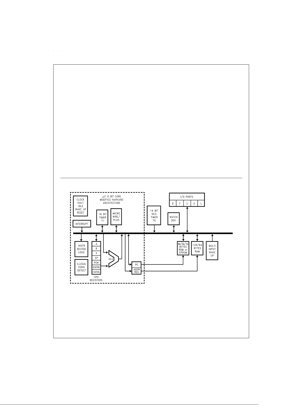
Block Diagram
DS012838-1
FIGURE 1. COP8SAx Block Diagram
www.national.com 2

General Description (Continued)
Key features include an 8-bit memory mapped architecture,
a 16-bit timer/counter with two associated 16-bit registers
supporting three modes (Processor Independent PWM generation, External Event counter, and Input Capture capabilities), two power saving HALT/IDLE modes with a
multi-sourced wakeup/interrupt capability, on-chip R/C oscillator, high current outputs, user selectable options such as
WATCHDOG, Oscillator configuration, and power-on-reset.
1.1 EMI REDUCTION
The COP8SAx family of devices incorporates circuitry that
guards against electromagnetic interference — an increasing
problem in today’s microcontroller board designs. National’s
patented EMI reduction technology offers low EMI clock circuitry,gradual turn-on output drivers (GTOs)and internal I
CC
smoothing filters, to helpcircumvent manyof the EMI issues
influencing embedded control designs. National has
achieved 15 dB–20 dB reduction in EMI transmissionswhen
designs have incorporated its patented EMI reducing circuitry.
1.2 ARCHITECTURE
The COP8SAx family is based on a modified Harvard architecture, which allows data tables to be accessed directly
from program memory. This is very important with modern
microcontroller-based applications, since program memory
is usually ROM or EPROM, while data memory is usually
RAM. Consequently data tables usually need to be contained in ROM or EPROM, so they are not lost when the microcontroller is powered down. In a modified Harvard architecture, instruction fetch and memory data transfers can be
overlapped with a two stage pipeline, which allows the next
instruction to be fetched from program memory while the
current instruction is being executed using data memory.
This is not possible witha Von Neumann single-addressbus
architecture.
The COP8SAx family supports a software stack scheme that
allows the user to incorporate many subroutine calls. This
capability is important when using High Level Languages.
With a hardware stack, the user is limited to a small fixed
number of stack levels.
1.3 INSTRUCTION SET
In today’s 8-bit microcontroller application arena cost/
performance, flexibility and time to market are several of the
key issues that system designers face in attempting to build
well-engineered products that compete in the marketplace.
Many of these issuescan be addressed through themanner
in which a microcontroller’s instruction set handles processing tasks. And that’s why COP8 family offers a unique and
code-efficient instruction set — one that provides the flexibility,functionality, reduced costs and faster time tomarket that
today’s microcontroller based products require.
Code efficiency is important because it enables designers to
pack more on-chip functionality into less program memory
space (ROM/OTP). Selecting a microcontroller with less program memory size translates into lower system costs, and
the added security of knowing that more code can be packed
into the available program memory space.
1.3.1 Key Instruction Set Features
The COP8SAx family incorporates a unique combination of
instruction set features, which provide designers with optimum code efficiency and program memory utilization.
Single Byte/Single Cycle Code Execution
The efficiency is due to the fact that the majority of instructions are of thesingle bytevariety, resulting in minimumprogram space. Because compact code does not occupya substantial amount of program memory space, designers can
integrate additional features and functionality into the microcontroller program memory space. Also, the majorityinstructions executed by the device are single cycle, resulting in
minimum program execution time. In fact, 77%of the instructions are single byte single cycle, providing greatercode and
I/O efficiency, and faster code execution.
1.3.2 Many Single-Byte, Multifunction Instructions
The COP8SAx instruction set utilizesmany single-byte, multifunction instructions. This enablesa single instruction to accomplish multiple functions, such as DRSZ,DCOR, JID, and
LOAD/EXCHANGE instructions with post-incrementing and
post-decrementing, to name just a few examples. In many
cases, the instruction set can simultaneously execute as
many as three functions with the same single-byte instruction.
JID: (Jump Indirect); Single byte instruction; decodes external events and jumps to corresponding service routines
(analogous to “DO CASE” statements in higher level languages).
LAID: (Load Accumulator-Indirect); Single byte look up table
instruction provides efficient data path from the program
memory to the CPU. This instruction can be used for table
lookup and to read the entire program memory for checksum
calculations.
RETSK: (Return Skip); Single byte instruction allows return
from subroutine and skips next instruction. Decision to
branch can be made in the subroutine itself, saving code.
AUTOINC/DEC: (Auto-Increment/Auto-Decrement); These
instructions use the two memory pointers B and X to efficiently process a block of data (analogousto “FOR NEXT” in
higher level languages).
1.3.3 Bit-Level Control
Bit-level control over many of the microcontroller’s I/O ports
provides a flexiblemeans to ease layout concernsand save
board space. All members of the COP8 family provide the
ability to set, reset and test any individual bit in the data
memory address space, including memory-mapped I/O ports
and associated registers. Three memory-mapped pointers
handle register indirect addressing and software stack
pointer functions. The memory data pointers allow the option
of post-incrementing or post-decrementing with the data
movement instructions (LOAD/EXCHANGE). And 15
memory-maped registers allow designers to optimize the
precise implementation of certain specific instructions.
1.4 PACKAGING/PIN EFFICIENCY
Real estate and board configuration considerations demand
maximum space and pin efficiency, particularly given today’s
high integration and small product form factors. Microcontroller users try to avoid using large packages to get the I/O
needed. Large packages take valuable board space and increases device cost, two trade-offs that microcontroller designs can ill afford.
The COP8 family offersa wide range of packages and do not
waste pins: up to 90.9%(or 40 pins in the 44-pin package)
are devoted to useful I/O.
www.national.com3
Connection Diagrams
DS012838-2
Top View
DS012838-3
Top View
DS012838-4
Top View
DS012838-39
Top View
DS012838-5
Top View
DS012838-6
Top View
FIGURE 2. Connection Diagrams
www.national.com 4
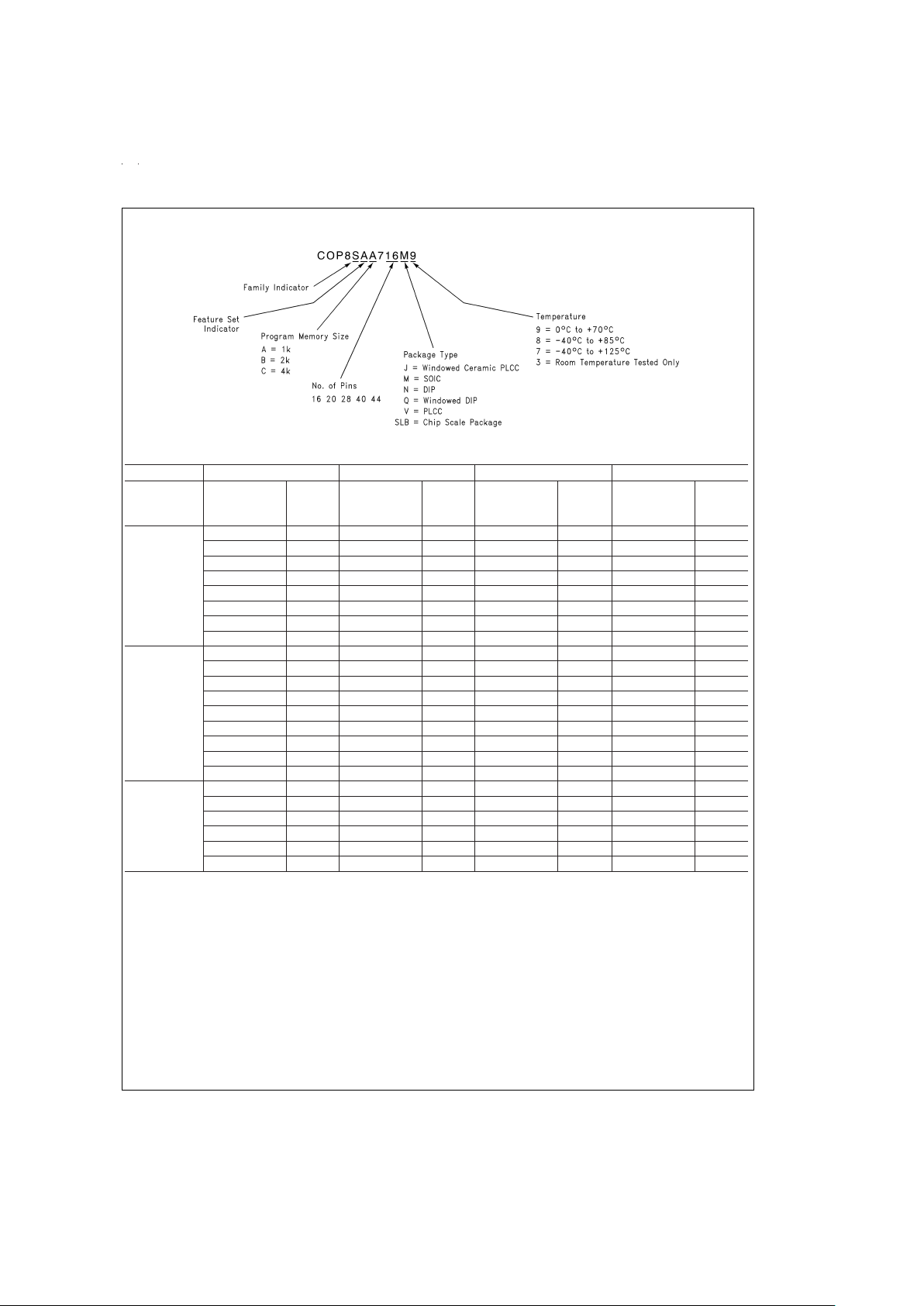
Ordering Information
1k EPROM 2k EPROM 4k EPROM 4k EPROM
Windowed
Device
Temperature Order Number Package Order Number Package Order Number Package Order Number Package
0˚C to +70˚C COP8SAA716M9 16M
COP8SAA720M9 20M COP8SAB720M9 20M COP8SAC720M9 20M
COP8SAA728M9 28M COP8SAB728M9 28M COP8SAC728M9 28M
COP8SAA716N9 16N
COP8SAA720N9 20N COP8SAB720N9 20N COP8SAC720N9 20N COP8SAC720Q3 20Q
COP8SAA728N9 28N COP8SAB728N9 28N COP8SAC728N9 28N COP8SAC728Q3 28Q
COP8SAC740N9 40N COP8SAC740Q3 40Q
COP8SAC744V9 44V COP8SAC744J3 44J
−40˚C to +85˚C COP8SAA716M8 16M
COP8SAA720M8 20M COP8SAB720M8 20M COP8SAC720M8 20M
COP8SAA728M8 28M COP8SAB728M8 28M COP8SAC728M8 28M
COP8SAA716N8 16N
COP8SAA720N8 20N COP8SAB720N8 20N COP8SAC720N8 20N
COP8SAA728N8 28N COP8SAB728N8 28N COP8SAC728N8 28N
COP8SAC740N8 40N
COP8SAC744V8 44V
COP8SAA7SLB8 SLB COP8SAB7SLB8 SLB COP8SAC7SLB8 SLB
−40˚C to
+125˚C
COP8SAC720M7 20M
COP8SAC728M7 28M
COP8SAC720N7 20N
COP8SAC728N7 28N
COP8SAC740N7 40N
COP8SAC744V7 44V
DS012838-8
FIGURE 3. Part Numbering Scheme
www.national.com5
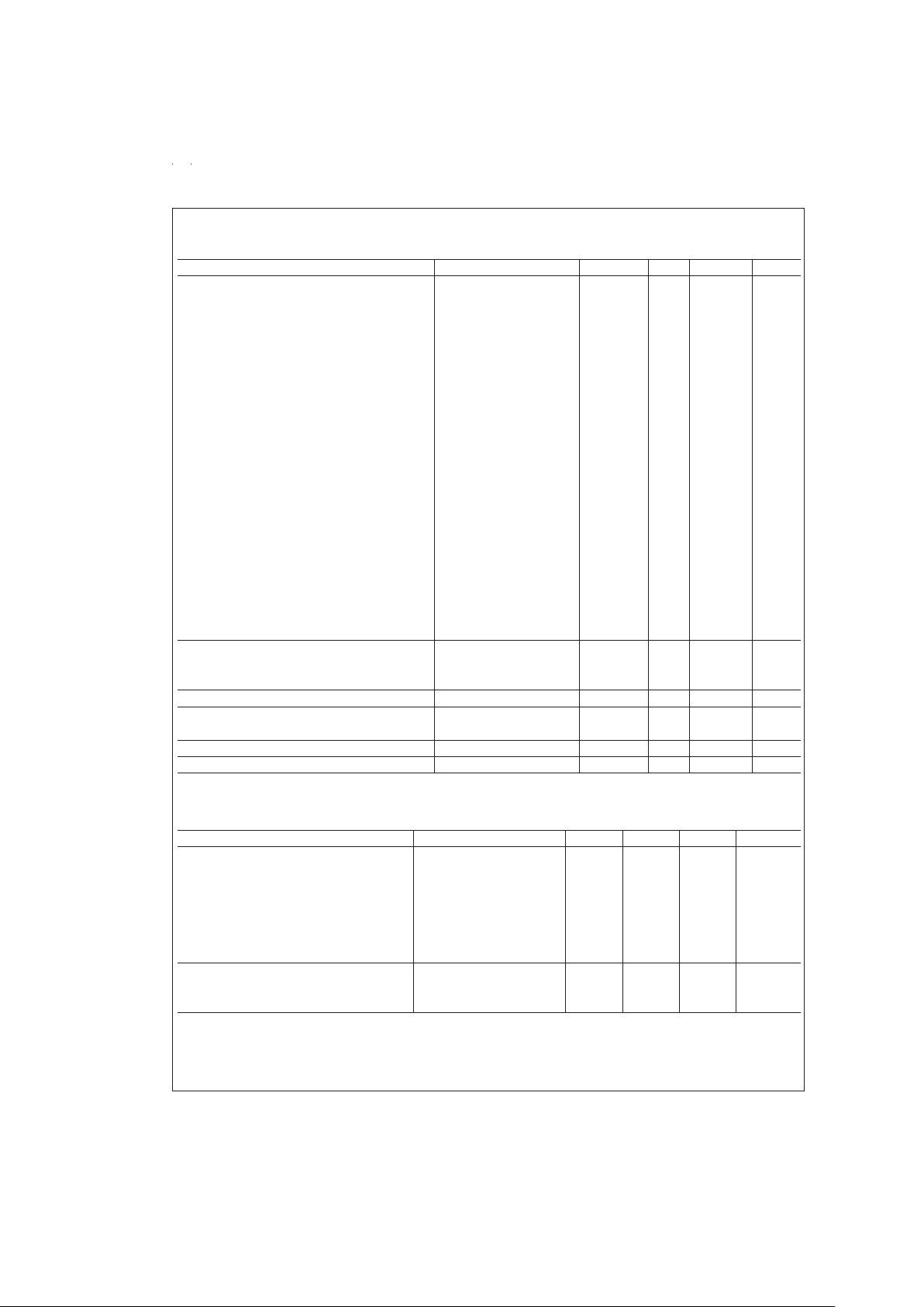
4.0 Electrical Characteristics
Absolute Maximum Ratings
(Note 1)
If Military/Aerospace specified devices are required,
please contact the National Semiconductor Sales Office/
Distributors for availability and specifications.
Supply Voltage (V
CC
)7V
Voltage at Any Pin −0.6V to V
CC
+0.6V
ESD Protection Level 2 kV
(Human Body Model)
Total Current into V
CC
Pin (Source) 80 mA
Total Current out of GND Pin (Sink) 100 mA
Storage Temperature Range −65˚C to +140˚C
Note 1:
Absolute maximum ratings indicate limits beyond which damage to
the device may occur. DC and AC electrical specifications are not ensured
when operating the device at absolute maximum ratings.
DC Electrical Characteristics
0˚C ≤ TA≤ +70˚C unless otherwise specified.
Parameter Conditions Min Typ Max Units
Operating Voltage (Note 8) 2.7 5.5 V
Power Supply Rise Time from 0.0V
(On-Chip Power-On Reset Selected) 10 ns 50 ms
V
CC
Start Voltage to Guarantee POR 0.25 V
Power Supply Ripple (Note 3) Peak-to-Peak 0.1 V
CC
V
Supply Current (Note 4)
CKI=10 MHz V
CC
=
5.5V, t
C
=
1µs 6 mA
CKI=4 MHz V
CC
=
4.5V, t
C
=
2.5 µs 2.1 mA
HALT Current (Note 5) —WATCHDOG Disabled V
CC
=
5.5V, CKI=0 MHz
<
48 µA
IDLE Current (Note 4)
CKI=10 MHz V
CC
=
5.5V, t
C
=
1 µs 1.5 mA
CKI=4 MHz V
CC
=
4.5V, t
C
=
2.5 µs 0.8 mA
Input Levels (V
IH,VIL
)
RESET
Logic High 0.8 V
CC
V
Logic Low 0.2 V
CC
V
CKI, All Other Inputs
Logic High 0.7 V
CC
V
Logic Low 0.2 V
CC
V
Value of the Internal Bias Resistor 0.5 1.0 2.0 MΩ
for the Crystal/Resonator Oscillator
CKI Resistance to V
CC
or GND when R/C V
CC
=
5.5V 5 8 11 kΩ
Oscillator is Selected
Hi-Z Input Leakage (same as TRI-STATE output) V
CC
=
5.5V −2 +2 µA
Input Pullup Current V
CC
=
5.5V, V
IN
=
0V −40 −250 µA
G and L Port Input Hysteresis 0.25 V
CC
V
www.national.com 6
DC Electrical Characteristics (Continued)
0˚C ≤ TA≤ +70˚C unless otherwise specified.
Parameter Conditions Min Typ Max Units
Output Current Levels
D Outputs
Source V
CC
=
4.5V, V
OH
=
3.3V −0.4 mA
V
CC
=
2.7V, V
OH
=
1.8V −0.2 mA
Sink V
CC
=
4.5V, V
OL
=
1.0V 10 mA
V
CC
=
2.7V, V
OL
=
0.4V 2 mA
L Port
Source (Weak Pull-Up) V
CC
=
4.5V, V
OH
=
2.7V −10 −110 µA
V
CC
=
2.7V, V
OH
=
1.8V −2.5 −33 µA
Source (Push-Pull Mode) V
CC
=
4.5V, V
OH
=
3.3V −0.4 mA
V
CC
=
2.7V, V
OH
=
1.8V −0.2 mA
Sink (L0–L3, Push-Pull Mode) V
CC
=
4.5V, V
OL
=
1.0V 10 mA
V
CC
=
2.7V, V
OL
=
0.4V 2 mA
Sink (L4–L7, Push-Pull Mode) V
CC
=
4.5V, V
OL
=
0.4V 1.6 mA
V
CC
=
2.7V, V
OL
=
0.4V 0.7 mA
All Others
Source (Weak Pull-Up Mode) V
CC
=
4.5V, V
OH
=
2.7V −10 −110 µA
V
CC
=
2.7V, V
OH
=
1.8V −2.5 −33 µA
Source (Push-Pull Mode) V
CC
=
4.5V, V
OH
=
3.3V −0.4 mA
V
CC
=
2.7V, V
OH
=
1.8V −0.2 mA
Sink (Push-Pull Mode) V
CC
=
4.5V, V
OL
=
0.4V 1.6 mA
V
CC
=
2.7V, V
OL
=
0.4V 0.7 mA
Allowable Sink Current per Pin (Note 8)
D Outputs and L0 to L3 15 mA
All Others 3mA
Maximum Input Current without Latchup
±
200 mA
(Note 6)
RAM Retention Voltage, Vr 2.0 V
V
CC
Rise Time from a VCC≥ 2.0V (Note 9) 12 µs
Input Capacitance (Note 8) 7 pF
Load Capacitance on D2 (Note 8) 1000 pF
www.national.com7
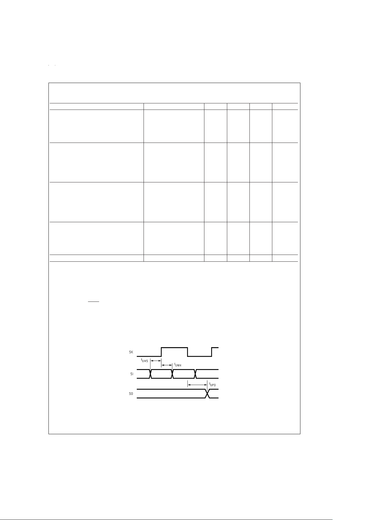
AC Electrical Characteristics
0˚C ≤ TA≤ +70˚C unless otherwise specified.
Parameter Conditions Min Typ Max Units
Instruction Cycle Time (t
C
)
Crystal/Resonator, External 4.5V ≤ V
CC
≤ 5.5V 1.0 DC µs
2.7V ≤ V
CC
<
4.5V 2.0 DC µs
Internal R/C Oscillator 4.5V ≤ V
CC
≤ 5.5V 2.0 µs
2.7V ≤ V
CC
<
4.5V TBD µs
R/C Oscillator Frequency Variation 4.5V ≤ V
CC
≤ 5.5V
±
35
%
(Note 8) 2.7V ≤ V
CC
<
4.5V TBD
%
External CKI Clock Duty Cycle (Note 8) fr=Max 45 55
%
Rise Time (Note 8) fr=10 MHz Ext Clock 12 ns
Fall Time (Note 8) fr=10 MHz Ext Clock 8 ns
Inputs
t
SETUP
4.5V ≤ VCC≤ 5.5V 200 ns
2.7V ≤ V
CC
<
4.5V 500 ns
t
HOLD
4.5V ≤ VCC≤ 5.5V 60 ns
2.7V ≤ V
CC
<
4.5V 150 ns
Output Propagation Delay (Note 7) R
L
=
2.2k, C
L
=
100 pF
t
PD1,tPD0
SO, SK 4.5V ≤ VCC≤ 5.5V 0.7 µs
2.7V ≤ V
CC
<
4.5V 1.75 µs
All Others 4.5V ≤ V
CC
≤ 5.5V 1.0 µs
2.7V ≤ V
CC
<
4.5V 2.5 µs
MICROWIRE Setup Time (t
UWS
) (Note 7) 20 ns
MICROWIRE Hold Time (t
UWH
) (Note 7) 56 ns
MICROWIRE Output Propagation Delay (t
UPD
) 220 ns
MICROWIRE Maximum Shift Clock
Master Mode 500 kHz
Slave Mode 1 MHz
Input Pulse Width (Note 7)
Interrupt Input High Time 1 t
C
Interrupt Input Low Time 1 t
C
Timer 1 Input High Time 1 t
C
Timer 1 Input Low Time 1 t
C
Reset Pulse Width 1 µs
Note 2: t
C
=
Instruction cycle time (Clock input frequency divided by 10).
Note 3: Maximum rate of voltage change must be
<
0.5 V/ms.
Note 4: Supply and IDLE currents are measured with CKI driven with a square wave Oscillator, CKO driven 180˚ out of phase with CKI, inputs connected to V
CC
and outputs driven low but not connected to a load.
Note 5: TheHALT mode will stop CKI from oscillating in the R/C and the Crystal configurations. In the R/C configuration, CKI is forced high internally. In the crystal
or external configuration, CKI is TRI-STATE. Measurement of I
DD
HALT is done with device neither sourcingnor sinking current; with L. F, C, G0, and G2–G5 pro-
grammed as low outputs and not driving a load; all outputs programmed low and not driving a load; all inputs tied to V
CC
; WATCHDOGand clock monitor disabled.
Parameter refers to HALT mode entered via setting bit 7 of the G Port data register.
Note 6: PinsG6 and RESET are designed with a high voltage input network. These pins allow input voltages
>
VCCand the pins will have sink current to VCCwhen
biased at voltages>VCC(the pins do not have source current when biasedat a voltage below VCC). The effective resistance to VCCis 750Ω (typical). These two
pins will not latch up. The voltage at the pins must be limited to
<
14V.WARNING: Voltages in excess of 14V will cause damage to the pins. This warning ex-
cludes ESD transients.
Note 7: The output propagation delay is referenced to the end of the instruction cycle where the output change occurs.
Note 8: Parameter characterized but not tested.
Note 9: Rise times faster than this specification may reset the device if POR is enabled and may affectthe value of IdleTimer T0 if POR is not enabled.
www.national.com 8
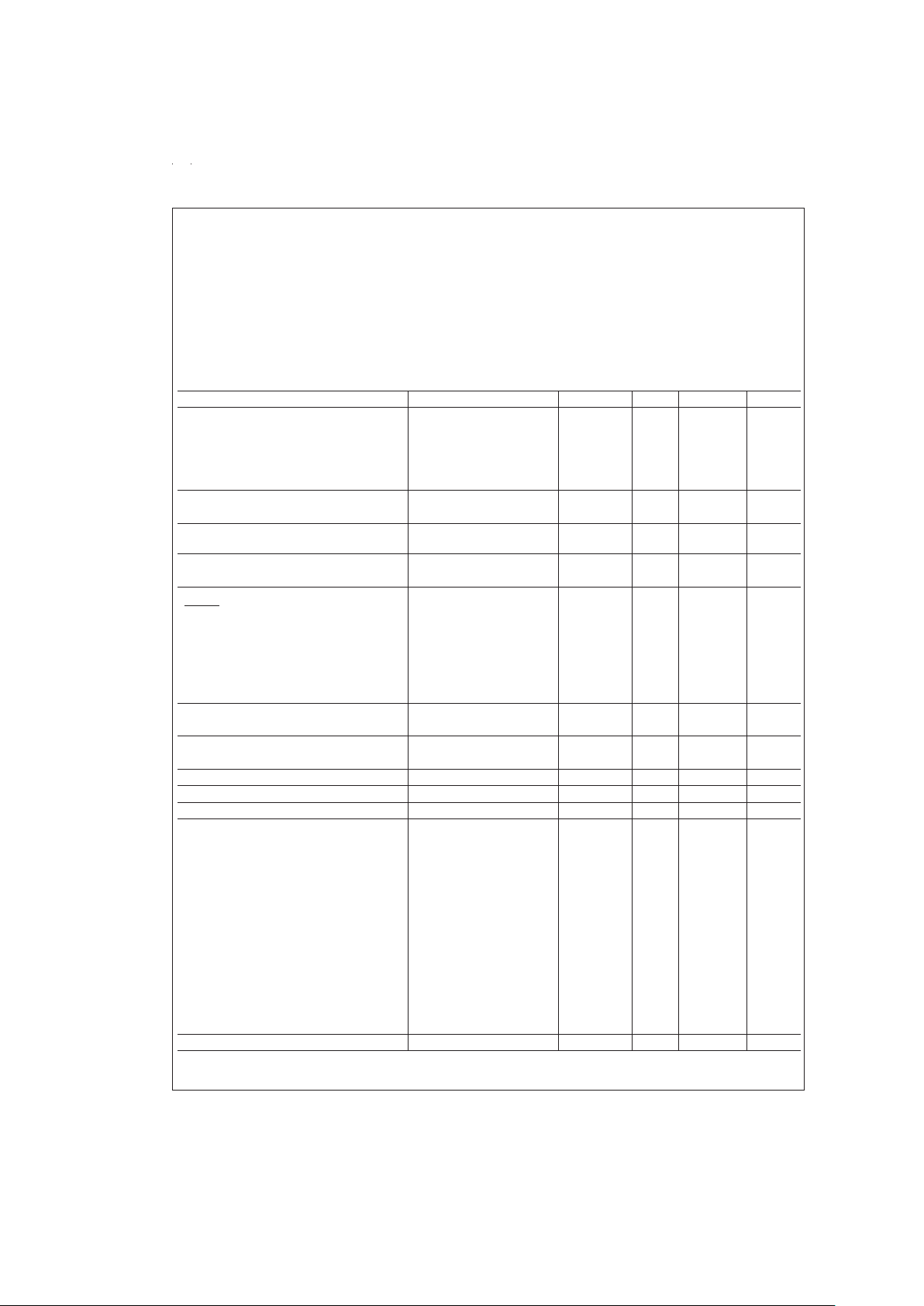
Absolute Maximum Ratings (Note 10)
If Military/Aerospace specified devices are required,
please contact the National Semiconductor Sales Office/
Distributors for availability and specifications.
Supply Voltage (V
CC
)7V
Voltage at Any Pin −0.6V to V
CC
+0.6V
ESD Protection Level 2 kV
(Human Body Model)
Total Current into V
CC
Pin (Source) 80 mA
Total Current out of GND Pin (Sink) 100 mA
Storage Temperature Range −65˚C to +140˚C
Note 10:
Absolute maximum ratings indicate limits beyond which damage to
the device may occur. DC and AC electrical specifications are not ensured
when operating the device at absolute maximum ratings.
DC Electrical Characteristics
−40˚C ≤ TA≤ +85˚C unless otherwise specified.
Parameter Conditions Min Typ Max Units
Operating Voltage 2.7 5.5 V
Power Supply Rise Time from 0.0V (Note 17)
(On-Chip Power-On Reset Selected) 10 ns 50 ms
V
CC
Start Voltage to Guarantee POR 0.25 V
Power Supply Ripple (Note 12) Peak-to-Peak 0.1 V
CC
V
Supply Current (Note 13)
CKI=10 MHz V
CC
=
5.5V, t
C
=
1 µs 6.0 mA
HALT Current (Note 14) —WATCHDOG Disabled V
CC
=
5.5V, CKI=0 MHz
<
4 10.0 µA
IDLE Current (Note 13)
CKI=10 MHz V
CC
=
5.5V, t
C
=
1 µs 1.5 mA
Input Levels (V
IH,VIL
)
RESET
Logic High 0.8 V
CC
V
Logic Low 0.2 V
CC
V
CKI, All Other Inputs
Logic High 0.7 V
CC
V
Logic Low 0.2 V
CC
V
Value of the Internal Bias Resistor 0.5 1.0 2.0 MΩ
for the Crystal/Resonator Oscillator
CKI Resistance to V
CC
or GND when R/C V
CC
=
5.5V 5 8 11 kΩ
Oscillator is Selected
Hi-Z Input Leakage (same as TRI-STATE output) V
CC
=
5.5V −2 +2 µA
Input Pullup Current V
CC
=
5.5V, V
IN
=
0V −40 −250 µA
G and L Port Input Hysteresis 0.25 V
CC
V
www.national.com9
DC Electrical Characteristics (Continued)
−40˚C ≤ TA≤ +85˚C unless otherwise specified.
Parameter Conditions Min Typ Max Units
Output Current Levels
D Outputs
Source V
CC
=
4.5V, V
OH
=
3.3V −0.4 mA
V
CC
=
2.7V, V
OH
=
1.8V −0.2 mA
Sink V
CC
=
4.5V, V
OL
=
1.0V 10 mA
V
CC
=
2.7V, V
OL
=
0.4V 2 mA
L Port
Source (Weak Pull-Up) V
CC
=
4.5V, V
OH
=
2.7V −10.0 −110 µA
V
CC
=
2.7V, V
OH
=
1.8V −2.5 −33 µA
Source (Push-Pull Mode) V
CC
=
4.5V, V
OH
=
3.3V −0.4 mA
V
CC
=
2.7V, V
OH
=
1.8V −0.2 mA
Sink (L0–L3, Push-Pull Mode) V
CC
=
4.5V, V
OL
=
1.0V 10.0 mA
V
CC
=
2.7V, V
OL
=
0.4V 2 mA
Sink (L4–L7, Push-Pull Mode) V
CC
=
4.5V, V
OL
=
0.4V 1.6 mA
V
CC
=
2.7V, V
OL
=
0.4V 0.7 mA
All Others
Source (Weak Pull-Up Mode) V
CC
=
4.5V, V
OH
=
2.7V −10.0 −110 µA
V
CC
=
2.7V, V
OH
=
1.8V −2.5 −33 µA
Source (Push-Pull Mode) V
CC
=
4.5V, V
OH
=
3.3V −0.4 mA
V
CC
=
2.7V, V
OH
=
1.8V −0.2 mA
Sink (Push-Pull Mode) V
CC
=
4.5V, V
OL
=
0.4V 1.6 mA
V
CC
=
2.7V, V
OL
=
0.4V 0.7 mA
Allowable Sink Current per Pin (Note 17)
D Outputs and L0 to L3 15 mA
All Others 3mA
Maximum Input Current without Latchup (Note 15)
±
200 mA
RAM Retention Voltage, Vr 2.0 V
V
CC
Rise Time from a VCC≥ 2.0V (Note 18) 12 µs
Input Capacitance (Note 17) 7 pF
Load Capacitance on D2 (Note 17) 1000 pF
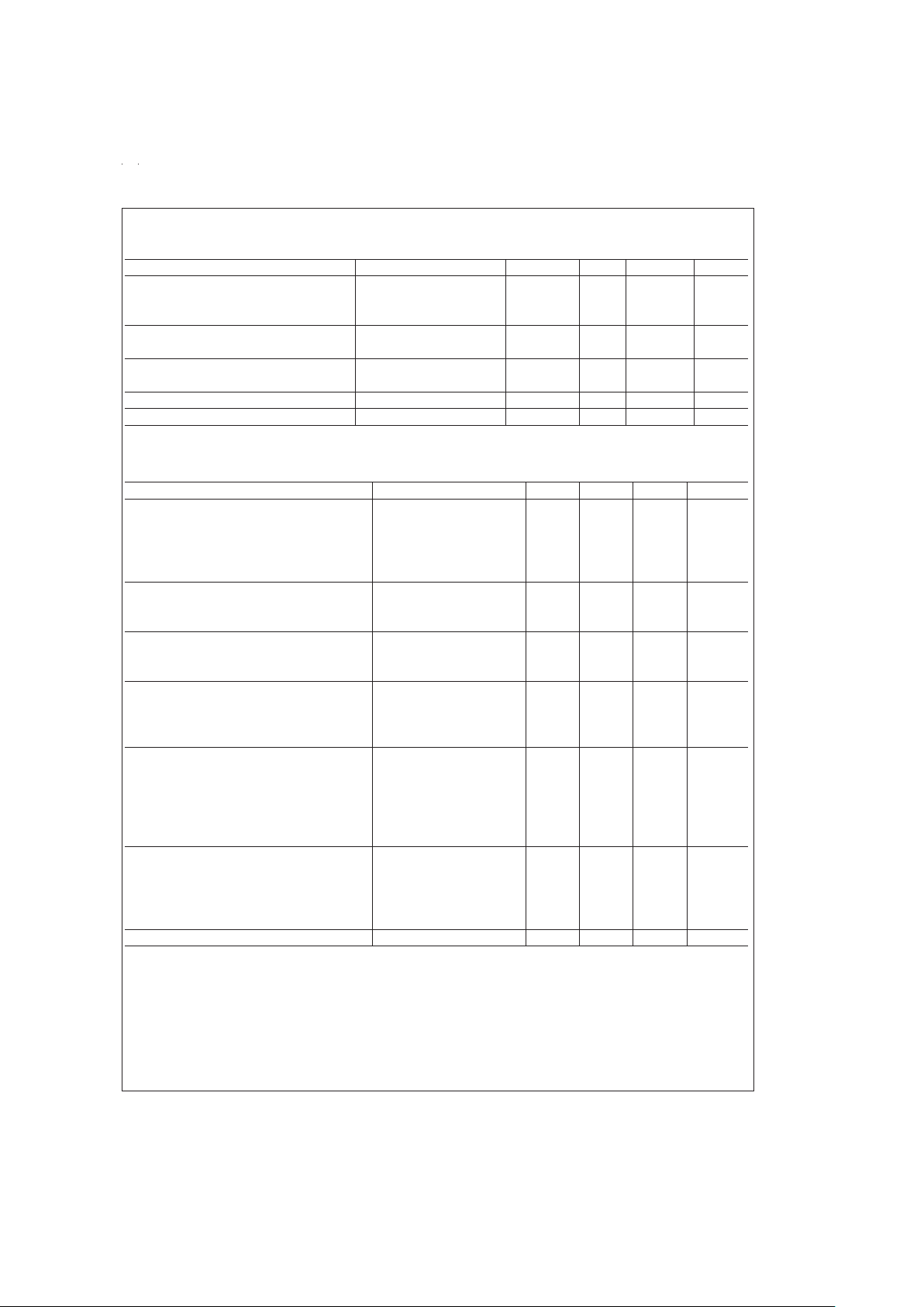
AC Electrical Characteristics
−40˚C ≤ TA≤ +85˚C unless otherwise specified.
Parameter Conditions Min Typ Max Units
Instruction Cycle Time (t
C
)
Crystal/Resonator, External 4.5V ≤ V
CC
≤ 5.5V 1.0 DC µs
2.7V ≤ V
CC
<
4.5V 2.0 DC µs
Internal R/C Oscillator 4.5V ≤ V
CC
≤ 5.5V 2.0 µs
2.7V ≤ V
CC
<
4.5V TBD µs
R/C Oscillator Frequency Variation 4.5V ≤ V
CC
≤ 5.5V
±
35
%
(Note 17) 2.7V ≤ V
CC
<
4.5V TBD
%
External CKI Clock Duty Cycle (Note 17) fr=Max 45 55
%
Rise Time (Note 17) fr=10 MHz Ext Clock 12 ns
Fall Time (Note 17) fr=10 MHz Ext Clock 8 ns
www.national.com 10
AC Electrical Characteristics (Continued)
−40˚C ≤ TA≤ +85˚C unless otherwise specified.
Parameter Conditions Min Typ Max Units
Inputs
t
SETUP
4.5V ≤ VCC≤ 5.5V 200 ns
2.7V ≤ V
CC
<
4.5V 500 ns
t
HOLD
4.5V ≤ VCC≤ 5.5V 60 ns
2.7V ≤ V
CC
<
4.5V 150 ns
Output Propagation Delay (Note 16) R
L
=
2.2k, C
L
=
100 pF
t
PD1,tPD0
SO, SK 4.5V ≤ VCC≤ 5.5V 0.7 µs
2.7V ≤ V
CC
<
4.5V 1.75 µs
All Others 4.5V ≤ V
CC
≤ 5.5V 1.0 µs
2.7V ≤ V
CC
<
4.5V 2.5 µs
MICROWIRE Setup Time (t
UWS
) (Note 16) 20 ns
MICROWIRE Hold Time (t
UWH
) (Note 16) 56 ns
MICROWIRE Output Propagation Delay (t
UPD
) 220 ns
MICROWIRE Maximum Shift Clock
Master Mode 500 kHz
Slave Mode 1 MHz
Input Pulse Width (Note 17)
Interrupt Input High Time 1 t
C
Interrupt Input Low Time 1 t
C
Timer 1 Input High Time 1 t
C
Timer 1 Input Low Time 1 t
C
Reset Pulse Width 1 µs
Note 11: t
C
=
Instruction cycle time (Clock input frequency divided by 10).
Note 12: Maximum rate of voltage change must be
<
0.5 V/ms.
Note 13: Supply and IDLE currents are measured with CKI driven with a square wave Oscillator, CKO driven 180˚ out of phase with CKI, inputs connected to V
CC
and outputs driven low but not connected to a load.
Note 14: TheHALTmode will stop CKI from oscillating in the R/C and the Crystal configurations. In the R/C configuration, CKI is forced high internally.In the crystal
or external configuration, CKI is TRI-STATE. Measurement of I
DD
HALT is done with device neither sourcingnor sinking current; with L. F, C, G0, and G2–G5 pro-
grammed as low outputs and not driving a load; all outputs programmed low and not driving a load; all inputs tied to V
CC
; clock monitor disabled. Parameter refers
to HALT mode entered via setting bit 7 of the G Port data register.
Note 15: PinsG6 and RESET are designed with a high voltage input network. These pins allow input voltages
>
VCCand the pins will have sink current to VCCwhen
biased at voltages>VCC(the pins do not have source current when biasedat a voltage below VCC). The effective resistance to VCCis 750Ω (typical). These two
pins will not latch up. The voltage at the pins must be limited to
<
14V.WARNING: Voltages in excess of 14V will cause damage to the pins. This warning excludes
ESD transients.
Note 16: The output propagation delay is referenced to the end of the instruction cycle where the output change occurs.
Note 17: Parameter characterized but not tested.
Note 18: Rise times faster than this specification may reset the device if POR is enabled and may affectthe value of IdleTimer T0 if POR is not enabled.
DS012838-9
FIGURE 4. MICROWIRE/PLUS Timing
www.national.com11
Absolute Maximum Ratings (Note 19)
If Military/Aerospace specified devices are required,
please contact the National Semiconductor Sales Office/
Distributors for availability and specifications.
Supply Voltage (V
CC
)7V
Voltage at Any Pin −0.6V to V
CC
+0.6V
ESD Protection Level 2 kV
(Human Body Model)
Total Current into V
CC
Pin (Source) 80 mA
Total Current out of GND Pin (Sink) 100 mA
Storage Temperature Range −65˚C to +140˚C
Note 19:
Absolute maximum ratings indicate limits beyond which damage to
the device may occur. DC and AC electrical specifications are not ensured
when operating the device at absolute maximum ratings.
DC Electrical Characteristics
−40˚C ≤ TA≤ +125˚C unless otherwise specified.
Parameter Conditions Min Typ Max Units
Operating Voltage 4.5 5.5 V
Power Supply Rise Time from 0.0V (Note 17)
(On-Chip Power-On Reset Selected) 10 ns 50 ms
V
CC
Start Voltage to Guarantee POR 0.25 V
Power Supply Ripple (Note 12) Peak-to-Peak 0.1 V
CC
V
Supply Current (Note 13)
CKI=10 MHz V
CC
=
5.5V, t
C
=
1 µs 6.0 mA
HALT Current (Note 14) —WATCHDOG
Disabled
V
CC
=
5.5V, CKI=0 MHz
<
10 30 µA
IDLE Current (Note 13)
CKI=10 MHz V
CC
=
5.5V, t
C
=
1 µs 1.5 mA
Input Levels (V
IH,VIL
)
RESET
Logic High 0.8 V
CC
V
Logic Low 0.2 V
CC
V
CKI, All Other Inputs
Logic High 0.7 V
CC
V
Logic Low 0.2 V
CC
V
Value of the Internal Bias Resistor 0.5 1.0 2.0 MΩ
for the Crystal/Resonator Oscillator
CKI Resistance to V
CC
or GND when R/C V
CC
=
5.5V 5 8 11 kΩ
Oscillator is Selected
Hi-Z Input Leakage V
CC
=
5.5V −5 +5 µA
Input Pullup Current V
CC
=
5.5V, V
IN
=
0V −35 −400 µA
G and L Port Input Hysteresis 0.25 V
CC
V
Output Current Levels
D Outputs
Source V
CC
=
4.5V, V
OH
=
3.3V −0.4 mA
Sink V
CC
=
4.5V, V
OL
=
1.0V 9 mA
L Port
Source (Weak Pull-Up) V
CC
=
4.5V, V
OH
=
2.7V −9 −140 µA
Source (Push-Pull Mode) V
CC
=
4.5V, V
OH
=
3.3V −0.4 mA
Sink (L0–L3, Push-Pull Mode) V
CC
=
4.5V, V
OL
=
1.0V 9 mA
Sink (L4–L7, Push-Pull Mode) V
CC
=
4.5V, V
OL
=
0.4V 1.4 mA
All Others
Source (Weak Pull-Up Mode) V
CC
=
4.5V, V
OH
=
2.7V −9 −140 µA
Source (Push-Pull Mode) V
CC
=
4.5V, V
OH
=
3.3V −0.4 mA
Sink (Push-Pull Mode) V
CC
=
4.5V, V
OL
=
0.4V 1.4 mA
TRI-STATE Leakage V
CC
=
5.5V −5 +5 µA
www.national.com 12
DC Electrical Characteristics (Continued)
−40˚C ≤ TA≤ +125˚C unless otherwise specified.
Parameter Conditions Min Typ Max Units
Allowable Sink Current per Pin (Note 17)
D Outputs and L0 to L3 15 mA
All Others 3mA
Maximum Input Current without Latchup Room Temp
±
200 mA
(Note 15)
RAM Retention Voltage, Vr 2.0 V
V
CC
Rise Time from a VCC≥ 2.0V (Note 18) 12 µs
Input Capacitance (Note 17) 7 pF
Load Capacitance on D2 (Note 17) 1000 pF
AC Electrical Characteristics
−40˚C ≤ TA≤ +125˚C unless otherwise specified.
Parameter Conditions Min Typ Max Units
Instruction Cycle Time (t
C
)
Crystal/Resonator, External 4.5V ≤ V
CC
≤ 5.5V 1.0 DC µs
Internal R/C Oscillator 4.5V ≤ V
CC
≤ 5.5V 2.0 DC µs
R/C Oscillator Frequency Variation 4.5V ≤ V
CC
≤ 5.5V TBD
%
(Note 6)
External CKI Clock Duty Cycle (Note 6) fr=Max 45 55
%
Rise Time (Note 6) fr=10 MHz Ext Clock 12 ns
Fall Time (Note 6) fr=10 MHz Ext Clock 8 ns
Inputs
t
SETUP
4.5V ≤ VCC≤ 5.5V 200 ns
t
HOLD
4.5V ≤ VCC≤ 5.5V 60 ns
Output Propagation Delay (Note 5) R
L
=
2.2k, C
L
=
100 pF
t
PD1,tPD0
SO, SK 4.5V ≤ VCC≤ 5.5V 0.7 µs
All Others 4.5V ≤ V
CC
≤ 5.5V 1.0 µs
MICROWIRE Setup Time (t
UWS
) (Note 5) 20 ns
MICROWIRE Hold Time (t
UWH
) (Note 5) 56 ns
MICROWIRE Output Propagation Delay (t
UPD
) 220 ns
MICROWIRE Maximum Shift Clock
Master Mode 500 kHz
Slave Mode 1 MHz
Input Pulse Width (Note 6)
Interrupt Input High Time 1 t
C
Interrupt Input Low Time 1 t
C
Timer 1, 2, 3 Input High Time 1 t
C
Timer 1, 2, 3 Input Low Time 1 t
C
Reset Pulse Width 1 µs
www.national.com13
5.0 Pin Descriptions
COP8SAx I/O structure minimizes external component requirements. Software-switchable I/O enables designers to
reconfigure the microcontroller’s I/O functions with a
single instruction. Each individual I/O pin can be independently configured as an output pin low, an output high, an
input with high impedance or an inputwith a weak pull-up
device.A typical example is the use ofI/O pins as the keyboard matrix input lines. The input lines can be programmed with internal weak pull-ups so that the input
lines read logic high when the keys are all up. With a key
closure, the corresponding input line will read a logic zero
since the weak pull-up can easily be overdriven. When the
key is released, the internal weak pullupwill pull the input
line back to logic high. This flexibility eliminates the need
for external pull-up resistors. The Highcurrent options are
available for driving LEDs, motors and speakers. This
flexibility helps to ensure a cleaner design, with less external components and lower costs.Below is thegeneral description of all available pins.
V
CC
and GND are the power supply pins. All VCCand
GND pins must be connected.
CKI is the clock input. This can come from the Internal
R/C oscillator, external, or a crystal oscillator (in conjunction with CKO). See Oscillator Description section.
RESET is the master reset input. See Reset description
section.
The device contains four bidirectional 8-bit I/O ports (C, G,
L and F), where each individual bit may be independently
configured as an input (Schmitt trigger inputs on ports L
and G), output or TRI-STATE under program control.
Three data memory address locations are allocated for
each of these I/O ports. Each I/Oport has two associated
8-bit memory mapped registers, the CONFIGURATION
register and the output DATAregister. A memory mapped
address is also reserved for the input pins of each I/O
port. (See thememory map for the various addresses associated with the I/O ports.)
Figure 5
shows the I/O port
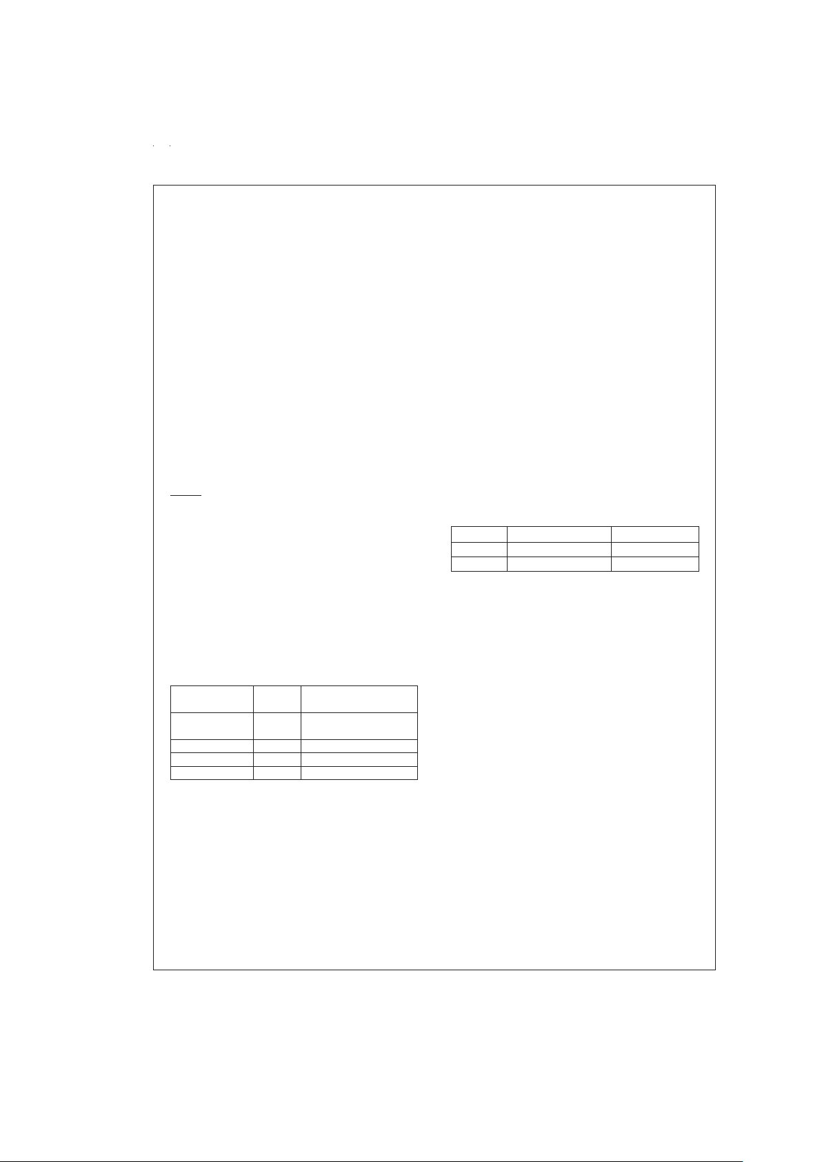
configurations. The DATA and CONFIGURATION registers allow for each port bit to be individually configured under software control as shown below:
CONFIGURATION DATA Port Set-Up
Register Register
0 0 Hi-Z Input
(TRI-STATE Output)
0 1 Input with Weak Pull-Up
1 0 Push-Pull Zero Output
1 1 Push-Pull One Output
Port L is an 8-bit I/O port. All L-pins haveSchmitt triggers on
the inputs.
Port L supports the Multi-Input Wake Up feature on all eight
pins. The 16-pin device does not have a full complement of
Port L pins. The unavailable pins are not terminated. Aread
operation these unterminated pins are not terminated.A read
operation these unterminated pins will return unpredictable
values. To minimize current drain, the unavailable pins must
be programmed as outputs.
Port G is an 8-bit port. Pin G0, G2–G5 are bi-directional I/O
ports. Pin G6 is always a general purposeHi-Z input. All pins
have Schmitt Triggers on theirinputs. Pin G1 serves as the
dedicated WDOUT WATCHDOG output with weakpullup
if WATCHDOG feature is selected by the ECON register.
The pin is a general purpose I/O if WATCHDOGfeature is
not selected. If WATCHDOG feature is selected, bit 1of the
Port G configuration anddata register does not have any effect on Pin G1 setup. Pin G7 is either input or output depending on the oscillator option selected. With the crystal oscillator option selected, G7 serves as the dedicated output pin for
the CKO clock output. With the internal R/C or the external
oscillator option selected, G7 serves as a general purpose
Hi-Z input pin and is also used to bring the device out of
HALT mode with a low to high transition on G7. There are
two registers associated with Port G, a data register and a
configuration register. Using these registers, each of the 5
I/O pins (G0, G2–G5) can be individually configured under
software control.
Since G6 is an input only pin and G7 is the dedicated CKO
clock output pin (crystal clock option) or general purpose input (R/C or external clock option), the associated bits in the
data and configuration registers for G6 and G7 are used for
special purpose functions as outlined below. Reading the G6
and G7 data bits will return zeroes.
The device will be placed in the HALT mode by writing a “1”
to bit 7 of the Port G Data Register. Similarly the device will
be placed in the IDLE mode by writing a “1” to bit 6 of the
Port G Data Register.
Writing a “1” to bit 6 of the Port G ConfigurationRegister enables the MICROWIRE/PLUS to operate with the alternate
phase of the SK clock. The G7 configuration bit, if set high,
enables the clock start up delay after HALT when the R/C
clock configuration is used.
Config. Reg. Data Reg.
G7 CLKDLY HALT
G6 Alternate SK IDLE
Port G has the following alternate features:
G6 SI (MICROWIRE Serial Data Input)
G5 SK (MICROWIRE Serial Clock)
G4 SO (MICROWIRE Serial Data Output)
G3 T1A (Timer T1 I/O)
G2 T1B (Timer T1 Capture Input)
G0 INTR (External Interrupt Input)
Port G has the following dedicated functions:
G7 CKO Oscillator dedicated output or general purpose in-
put
G1 WDOUTWATCHDOGand/or CLock Monitor if WATCH-
DOG enabled, otherwise it is a general purpose I/O
Port C is an 8-bit I/O port. The 40-pin device does not have
a full complement of Port C pins. The unavailable pins are
not terminated. A read operation on these unterminated pins
will return unpredictable values. Only the COP8SAC7 device
contains Port C. The 20/28 pin devices do not offer Port C.
On these devices, the associated Port C Data and Configuration registers should not be used.
Port F is an 8-bit I/O port. The 28-pin device does not have
a full complement of Port F pins. The unavailable pins are
not terminated. A read operation on these unterminated pins
will return unpredictable values.
www.national.com 14
5.0 Pin Descriptions (Continued)
Port D is an 8-bit output port that is preset high when RESET
goes low. The user can tie two or more D port outputs (except D2) together in order to get a higher drive.
Note: Care must be exercised with the D2 pin operation.At RESET, the ex-
ternal loads on this pin must ensure that the output voltages stay
above 0.7 V
CC
to prevent the chip from entering special modes.Also
keep the external loading on D2 to less than 1000 pF.
6.0 Functional Description
The architecture of the device is a modified Harvard architecture. With the Harvard architecture, the program memory
EPROM is separated from the data store memory (RAM).
Both EPROM and RAM have their own separate addressing
space with separate address buses. The architecture,
though based on the Harvard architecture, permits transfer
of data from EPROM to RAM.
6.1 CPU REGISTERS
The CPU can do an 8-bit addition, subtraction, logical or shift
operation in one instruction (t
C
) cycle time.
There are six CPU registers:
A is the 8-bit Accumulator Register
PC is the 15-bit Program Counter Register
PU is the upper 7 bits of the program counter (PC)
PL is the lower 8 bits of the program counter (PC)
B is an 8-bit RAM address pointer, which can be optionally
post auto incremented or decremented.
X is an 8-bit alternate RAM address pointer, which can be
optionally post auto incremented or decremented.
SP is the 8-bit stack pointer, which points to the subroutine/
interrupt stack (in RAM). With reset the SP is initialized to
RAM address 02F Hex (devices with 64 bytes of RAM), or
initialized to RAM address 06F Hex (devices with 128 bytes
of RAM).
All the CPU registers are memory mapped with the exception of the Accumulator (A) and the Program Counter (PC).
6.2 PROGRAM MEMORY
The program memory consists of 1024, 2048, or 4096 bytes
of EPROM or ROM.
Table 1
shows the program memory
sizes for the different devices. These bytes may hold program instructions or constant data (data tables for the LAID
instruction, jump vectors for theJID instruction, andinterrupt
vectors for the VIS instruction). The program memory is addressed by the 15-bit program counter (PC). All interrupts in
the device vector to programmemory location0FF Hex. The
contents of the program memory read 00 Hex in the erased
state.
6.3 DATA MEMORY
The data memory address space includes the on-chip RAM
and data registers, the I/O registers (Configuration, Data and
Pin), the control registers, the MICROWIRE/PLUS SIO shift
register, and the various registers, and counters associated
with the timers (with the exception of the IDLE timer). Data
memory is addressed directly by the instruction or indirectly
by the B, X and SP pointers.
The data memory consistsof 64or 128bytes of RAM.
Table
1
shows the data memory sizesfor thedifferent devices. Fifteen bytes of RAM are mapped as “registers” at addresses
0F0 to 0FE Hex. These registers can be loaded immediately,
and also decremented and tested with the DRSZ (decrement
register and skip if zero) instruction. The memory pointer
registers X, SP and B are memory mappedinto this space at
address locations 0FC to 0FE Hex respectively, with the
other registers (except 0FF) being available for general usage.Address location 0FF is reserved for future RAM expansion. If compatibility with future devices (with more RAM) is
not desired, this location can be used as a general purpose
RAM location.
DS012838-10
FIGURE 5. I/O Port Configurations
DS012838-12
FIGURE 6. I/O Port Configurations— Output Mode
DS012838-11
FIGURE 7. I/O Port Configurations— Input Mode
www.national.com15

6.0 Functional Description (Continued)
The instruction set permits any bitin memory to beset, reset
or tested. All I/O and registers (except A and PC) are
memory mapped; therefore,I/O bits and register bitscan be
directly and individually set, reset and tested. The accumulator (A) bits can also be directly and individually tested.
RAM contents are undefined upon power-up.
TABLE 1. Program/Data Memory Sizes
Program Data User
Device Memory Memory Storage
(Bytes) (Bytes) (Bytes)
COP8SAA7 1024 64 8
COP8SAB7 2048 128 8
COP8SAC7 4096 128 8
6.4 ECON (CONFIGURATION) REGISTER
The ECON register is used to configure the user selectable
clock, security, power-on reset, WATCHDOG, and HALT options. The register can be programmed and read only in
EPROM programming mode. Therefore, the register should
be programmed at the same time as the program memory.
The contents of the ECON register shipped from the factory
read 00 Hex (windowed device), 80 Hex (OTP device) or as
specified by the customer (ROM device).
The format of the ECON register is as follows:
Bit 7 Bit 6 Bit 5 Bit 4 Bit 3 Bit 2 Bit 1 Bit 0
X POR SECURITY CKI 2 CKI 1 WATCH Reserved HALT
DOG
Bit 7=x This is for factory test. The polarity is al-
ways 0.
Bit 6=1 Power-on reset enabled.
=
0 Power-on reset disabled.
Bit 5=1 Security enabled. EPROM read and write
are not allowed.
=
0 Security disabled. EPROM read and write
are allowed.
Bits 4, 3=0, 0 External CKI option selected. G7 is avail-
able as a HALT restart and/or general purpose input. CKI is clock input.
=
0, 1 R/C oscillator option selected. G7 is avail-
able as a HALT restart and/or general purpose input. CKI clock input. Internal R/C
components are supplied for maximum
R/C frequency.
=
1, 0 Crystal oscillator with on-chip crystal bias
resistor disabled. G7 (CKO) is the clock
generator output to crystal/resonator.
=
1, 1 Crystal oscillator with on-chip crystal bias
resistor enabled. G7 (CKO) is the clock
generator output to crystal/resonator.
Bit 2=1 WATCHDOG feature disabled. G1 is a
general purpose I/O.
=
0 WATCHDOG feature enabled. G1 pin is
WATCHDOG output with waek pullup.
Bit 1
=
Reserved.
Bit 0=1 HALT mode disabled.
=
0 HALT mode enabled.
6.5 USER STORAGE SPACE IN EPROM
In addition to the ECON register, there are 8 bytes of
EPROM available for “user information”. ECON and these 8
bytes are outside of the code area and are not protected by
the security bit of the ECON register. Even when security is
set, information in the 8-byte USER area is both read and
write enabled allowing the user to read from and write into
the area at all times while still protecting the code fromunauthorized access.
Both ECON and USER area,9 bytes total,are outside of the
normal address range of the EPROM and can not be accessed by the executing software. This allows for the storage of non-secured information. Typical uses arefor storage
of serial numbers, data codes, version numbers, copyright
information, lot numbers, etc.
The COP8 assembler defines a special ROM section type,
CONF, into which theECON and USER data may be coded.
Both ECON and User Data are programmed automatically
by programmers that are certified by National.
The following examples illustrate the declaration of ECON
and the User information.
Syntax:
[label:] .sect econ, conf
.db value ;1 byte,
;configures options
.db
.endsect<user information>
;up to 8 bytes
Example: The following sets a value in the ECON register
and User Identification for a COP8SAC728M7. The ECON
bit values shown selectoptions: Power-on enabled,Security
disabled, Crystal oscillator with on-chip bias disabled,
WATCHDOG enabled and HALT mode enabled.
.chip 8SAC
.sect econ, conf
.db 0x55 ;por, extal, wd, halt
.db 'my v1.00' ;user data declaration
.endsect
...
.end start
Note: All programmers certified for programming this family of parts will sup-
port programming of the CONFiguration section. Please contact National or your device programmer supplier for more information.
6.6 OTP SECURITY
The device has a security feature that, when enabled, prevents external reading of theOTP program memory.The security bit in the ECON register determines, whether security
is enabled or disabled. If the security feature is disabled, the
contents of the internal EPROM may be read.
If the security feature is enabled, thenany attempt to externally read the contents of the EPROM will result in the
value FF Hex beingread fromall program locations. Under no circumstances can a secured part be read. In ad-
dition, with the security feature enabled, the write operation
to the EPROM program memory and ECONregister is inhibited. The ECON register is readable regardless of the state
of the security bit. The security bit, when set, cannot be
erased, even in windowed packages. If the security bit is
set in a device in a windowed package, that device may be
erased but will not be further programmable.
If security is being used, itis recommended that allother bits
in the ECON register beprogrammed first.Then the security
bit can be programmed.
www.national.com 16
6.0 Functional Description (Continued)
6.7 RESET
The device is initialized whenthe RESET pinis pulled lowor
the On-chip Power-On Reset is enabled.
The following occurs upon initialization:
Port L: TRISTATE
Port C: TRISTATE
Port G: TRISTATE
Port F: TRISTATE
Port D: HIGH
PC: CLEARED to 0000
PSW, CNTRL and ICNTRL registers: CLEARED
SIOR: UNAFFECTED after RESET with power already
applied
RANDOM after RESET at power-on
T1CNTRL: CLEARED
Accumulator, Timer 1:
RANDOM after RESET with crystal clock option
(power already applied)
UNAFFECTED after RESET with R/C clock option
(power already applied)
RANDOM after RESET at power-on
WKEN, WKEDG: CLEARED
WKPND: RANDOM
SP (Stack Pointer):
Initialized to RAM address 02F Hex (devices with
64 bytes of RAM), or initialized to
RAM address 06F Hex (devices with
128 bytes of RAM).
B and X Pointers:
UNAFFECTED after RESET with power
already applied
RANDOM after RESET at power-on
RAM:
UNAFFECTED after RESET with power already
applied
RANDOM after RESET at power-on
WATCHDOG (if enabled):
The device comes out of reset with both the WATCHDOG
logic and the Clock Monitor detector armed, with the
WATCHDOG service window bits set and the Clock Monitor
bit set. The WATCHDOG and Clock Monitor circuits are inhibited during reset. The WATCHDOG service window bits
being initialized high default to the maximum WATCHDOG
service window of 64k t
C
clock cycles. The Clock Monitor bit
being initialized high will cause a Clock Monitor error following reset if the clock has not reached the minimum specified
frequency at the termination of reset. A Clock Monitor error
will cause an active low error output on pin G1. This error
output will continue until 16 t
C
–32 tCclock cycles following
the clock frequency reaching the minimum specified value,
at which time the G1 output will go high.
6.7.1 External Reset
The RESET input whenpulled lowinitializes thedevice. The
RESET pin must be held low for a minimum of one instruction cycle to guarantee a valid reset. During Power-Up initialization, the user mustensure thatthe RESET pin is heldlow
until the device is within the specified VCCvoltage. An R/C
circuit on the RESET pin with a delay 5 times (5x) greater
than the power supply rise time or 15 µs whichever is
greater,is recommended. Reset should also be wide enough
to ensure crystal start-up upon Power-Up.
RESET may also be used to cause an exit from the HALT
mode.
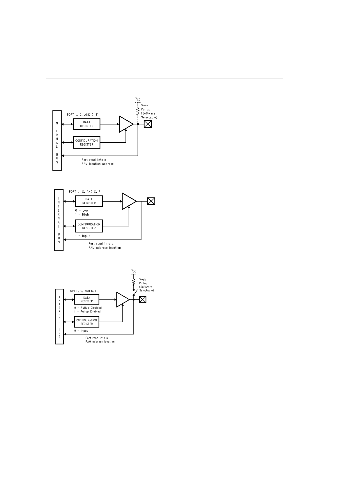
Arecommended reset circuit for this devicedis shown in
Fig-
ure 9
.
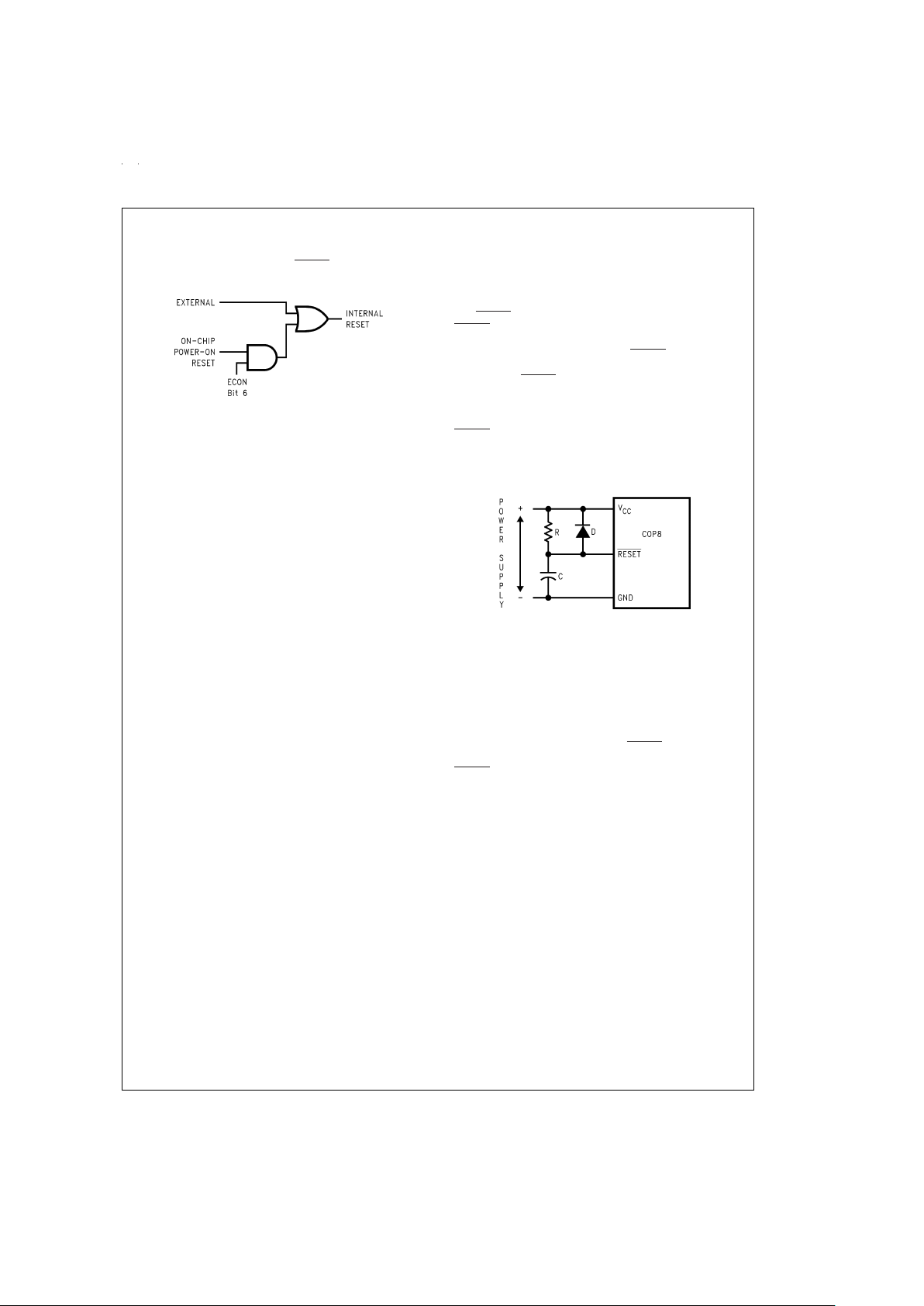
6.7.2 On-Chip Power-On Reset
The on-chip reset circuit is selected by a bit in the ECON register. When enabled, the device generates an internal reset
as V
CC
rises to a voltage level above 2.0V. The on-chipreset
circuitry is able to detect both fast and slow rise times on V
CC
(VCCrise time between 10 ns and 50 ms).
Under no circumstances should the RESET pin be allowed
to float. If the on-chip Power-On Reset feature isbeing used,
RESET pin should be connected directly to V
CC
. The output
of the power-on reset detector will always preset the Idle
timer to 0FFF(4096 t
C
). At this time, the internal reset will be
generated.
If the Power-On Reset feature is enabled, the internal reset
will not be turned offuntil the Idle timer underflows. The internal reset will perform the same functions as external reset.
The user is responsible for ensuring that V
CC
is at the mini-
mum level for the operating frequencywithin the 4096t
C
. After the underflow, the logic is designed such that no additional internal resets occur as long as V
CC
remains above
2.0V.
Note: While the POR feature of the COP8SAx was never intended to function
as a brownout detector, there are certainconstraints of this block that
the system designer must address to properly recover from a brownout
condition. This is true regardless of whether the internal POR or the
external reset feature is used.
A brownout condition is reached when V
CC
of the device goes below
the minimum operating conditions of the device. The minimum guaranteed operating conditions are defined as V
CC
= 4.5V@10 MHz CKI,
V
CC
= 2.7V@4 MHz, or VCC= 2.0V during HALT mode (or when CKI
is stopped) operation.
When using either the external reset or the POR feature to recover
from a brownout condition, V
CC
must be lowered to 0.25V or an external reset must be applied whenever it goes below the minimumoperating conditions as stated above.
DS012838-13
FIGURE 8. Reset Logic
DS012838-14
RC>5x power supply rise time or 15 µs, whichever is greater.
FIGURE 9. Reset Circuit Using External Reset
www.national.com17
6.0 Functional Description (Continued)
The contents of data registers and RAM are unknown following the on-chip reset.
6.8 OSCILLATOR CIRCUITS
There are four clock oscillator options available: Crystal Oscillator with or without on-chip bias resistor, R/C Oscillator
with on-chip resistor and capacitor, and External Oscillator.
The oscillator feature is selectedby programming theECON
register, which is summarized in
Table 2
.
TABLE 2. Oscillator Option
ECON4 ECON3 Oscillator Option
0 0 External Oscillator
1 0 Crystal Oscillator without Bias Resistor
0 1 R/C Oscillator
1 1 Crystal Oscillator with Bias Resistor
6.8.1 Crystal Oscillator
The crystal Oscillator mode can be selected by programming
ECON Bit 4 to 1. CKI is the clock input while G7/CKO is the
clock generator output to the crystal. An on-chip bias resistor
connected between CKI and CKO can be enabled by programming ECON Bit 3 to 1 with the crystal oscillator option
selection. The value of the resistor is in the range of 0.5M to
2M (typically 1.0M).
Table3
shows the component values required for various standard crystal values. Resistor R2 is
only used when the on-chip bias resistor is disabled.
Figure
12
shows the crystal oscillator connection diagram.
TABLE 3. Crystal Oscillator Configuration,
T
A
=
25˚C, V
CC
=
5V
R1 (kΩ)R2(MΩ) C1 (pF) C2 (pF) CKI Freq. (MHz)
0 1 30 30 15
0 1 32 32 10
0 1 45 30–36 4
5.6 1 100 100–156 0.455
6.8.2 External Oscillator
The External Oscillator mode can be selected by programming ECON Bit 3 to 0 and ECON Bit 4 to 0. CKI can be
driven by an external clock signal provided it meets the
specified duty cycle, rise andfall times,and input levels.G7/
CKO is available as a general purpose input G7 and/or Halt
control.
Figure 13
shows the external oscillator connection
diagram.
6.8.3 R/C Oscillator
The R/C Oscillator mode can be selected by programming
ECON Bit 3 to 1 and ECON Bit 4 to 0. In R/C oscillation
mode, CKI is left floating, while G7/CKO is available as a
general purpose input G7 and/or HALTcontrol. The R/C controlled oscillator has on-chip resistor and capacitor for maximum R/C oscillator frequency operation. The maximum frequency is 5 MHz
±
35%for VCCbetween 4.5V to 5.5V and
temperature range of −40˚C to +85˚C. For max frequency
operation, the CKI pin should be left floating. For lower frequencies, an external capacitor should be connected between CKI and either V
CC
or GND. Immunity of the R/C oscillator to external noise can be improved by connecting one
half the external capacitance to V
CC
and one half to GND.
PC board trace length on the CKI pin should be kept as short
as possible.
Table 4
shows the oscillator frequency as a
function of external capacitance on the CKI pin.
Figure 14
shows the R/C oscillator configuration.
TABLE 4. R/C Oscillator Configuration,
−40˚C to +85˚C, V
CC
=
4.5V to 5.5V,
OSC Freq. Variation of
±
35
%
External Capacitor R/C OSC Freq Instr. Cycle
(pF) (MHz) (µs)
0 5 2.0
9 4 2.5
52 2 5.0
150 1 10
TBD 32 kHz 312.5
DS012838-15
FIGURE 10. Reset Timing (Power-On Reset Enabled)
with V
CC
Tied to RESET
DS012838-16
FIGURE 11. Reset Circuit Using Power-On Reset
www.national.com 18
 Loading...