


NSC CLC449MDC, CLC449AMC, CLC449AJP, CLC449AJE-TR13, CLC449AJE Datasheet
...N June 1999
CLC449
1.1GHz Ultra-Wideband Monolithic Op Amp
General Description
The CLC449 is an ultra-high-speed monolithic op amp, with a typical -3dB bandwidth of 1.1GHz at a gain of +2. This wideband op amp supports rise and fall times less than 1ns, settling time of 6ns (to 0.2%) and slew rate of 2500V/µs. The CLC449 achieves 2nd harmonic distortion of -68dBc at 5MHz at a low supply current of only 12mA. These performance advantages have been achieved through improvements in National’s proven current feedback topology combined with a high-speed complementary bipolar process.
The DC to 1.2GHz bandwidth of the CLC449 is suitable for many IF and RF applications as a versatile op amp building block for replacement of AC coupled discrete designs. Operational amplifier functions such as active filters, gain blocks, differentiation, addition, subtraction and other signal conditioning functions take full advantage of the CLC449’s unity-gain stable closed-loop performance.
The CLC449 performance provides greater headroom for lower frequency applications such as component video, high-resolution workstation graphics, and LCD displays. The amplifier’s 0.1dB gain flatness to beyond 200MHz, plus 0.8ns 2V rise and fall times are ideal for improved time domain performance. In addition, the 0.03%/0.02° differential gain/phase performance allows system flexibility for handling standard NTSC and PAL signals.
In applications using high-speed flash A/D and D/A converters, the CLC449 provides the necessary wide bandwidth (1.1GHz), settling (6ns to 0.2%) and low distortion into 50Ω loads to improve SFDR.
Features
■1.1GHz small-signal bandwidth (Av = +2)
■2500V/µs slew rate
■0.03%, 0.02° DG, DΦ
■6ns settling time to 0.2%
■3rd order intercept, 30dBm @ 70MHz
■Dual ±5V or single 10V supply
■High output current: 90mA
■2.5dB noise figure
Applications
■High performance RGB video
■RF/IF amplifier
■Instrumentation
■Medical electronics
■Active filters
■High-speed A/D driver
■High-speed D/A buffer
Frequency Response (Av = +2V/V)
Wideband-Ultra 1GHz.1 |
CLC449 |
Amp Op Monolithic |
|
Typical Application
120MSPS High-Speed Flash ADC Driver
Pinout
DIP & SOIC
|
|
|
|
|
|
|
|
|
|
|
|
|
|
|
|
|
|
|
|
|
|
|
|
|
|
|
|
|
|
|
|
|
|
|
|
|
|
|
|
|
|
|
|
|
|
|
|
|
|
|
|
|
|
|
|
|
|
|
|
|
|
|
|
|
|
|
|
|
|
|
|
|
|
|
|
|
|
|
|
|
|
|
|
|
|
|
|
|
|
|
|
|
|
|
|
|
|
|
|
|
|
|
|
|
|
|
|
|
|
|
|
|
|
|
|
|
|
|
|
|
|
|
|
|
|
|
|
|
|
|
|
|
|
|
|
|
|
|
|
|
|
|
|
|
|
|
|
|
|
|
|
|
|
|
|
|
|
|
|
|
|
|
|
|
© 1999 National Semiconductor Corporation |
|
|
|
http://www.national.com |
||||||
|
|
|
||||||||
Printed in the U.S.A.

CLC449 Electrical Characteristics (Av = +2, Rf = 250Ω, Vcc = ±5V, R L = 100Ω; unless specified)
|
PARAMETERS |
CONDITIONS |
TYP |
|
MIN/MAX RATINGS |
UNITS |
NOTES |
||
|
|
|
|
|
|
|
|
|
|
|
|
CLC449 |
+25° |
+25° |
|
0° to +70° |
-40° to +85° |
|
|
|
|
|
|
|
|
|
|
|
|
|
FREQUENCY DOMAIN RESPONSE |
|
|
|
|
|
|
|
|
|
-3dB bandwidth |
|
|
|
|
|
|
|
|
|
small signal |
<0.2Vpp |
1100 |
|
|
|
|
MHz |
|
|
large signal |
<2Vpp |
500 |
380 |
|
380 |
360 |
MHz |
|
|
±0.1 dB bandwidth |
<2Vpp |
200 |
|
|
|
|
MHz |
|
|
gain flatness |
|
|
|
|
|
|
|
|
|
peaking |
DC to 200MHz |
0 |
|
|
|
|
dB |
|
|
rolloff |
DC to 200MHz |
0.1 |
0.5 |
|
0.5 |
0.5 |
dB |
|
|
linear phase deviation |
<200MHz |
0.8 |
|
|
|
|
deg |
|
|
differential gain |
4.43MHz, RL=150Ω |
0.03 |
0.05 |
|
0.05 |
0.05 |
% |
|
|
differential phase |
4.43MHz, RL=150Ω |
0.02 |
0.02 |
|
0.05 |
0.05 |
deg |
|
|
TIME DOMAIN RESPONSE |
|
|
|
|
|
|
|
|
|
rise and fall time |
2V step |
0.8 |
1.1 |
|
1.1 |
1.1 |
ns |
|
|
settling time to 0.2% |
2V step |
6 |
|
|
|
|
ns |
|
|
settling time to 0.1% |
2V step |
11 |
|
|
|
|
ns |
|
|
overshoot |
2V step |
10 |
18 |
|
18 |
18 |
% |
|
|
slew rate |
4V step |
2500 |
2000 |
|
2000 |
2000 |
V/µs |
|
|
|
|
|
|
|
|
|
|
|
|
DISTORTION AND NOISE RESPONSE |
|
|
|
|
|
|
|
|
|
2nd harmonic distortion |
2Vpp, 5MHz |
-63 |
59 |
|
59 |
59 |
dBc |
|
|
|
2Vpp, 20MHz |
-52 |
-48 |
|
-48 |
-48 |
dBc |
|
|
|
2Vpp, 50MHz |
-44 |
40 |
|
40 |
40 |
dBc |
|
|
3rd harmonic distortion |
2Vpp, 5MHz |
-84 |
77 |
|
75 |
75 |
dBc |
|
|
|
2Vpp, 20MHz |
-73 |
-66 |
|
-64 |
-64 |
dBc |
|
|
3rd order intercept |
2Vpp, 50MHz |
-62 |
55 |
|
53 |
53 |
dBc |
|
|
70MHz |
30 |
|
|
|
|
dBm |
|
|
|
1dB gain compression @ 50MHz |
|
16 |
|
|
|
|
dBm |
|
|
equivalent input noise |
|
|
|
|
|
|
nV/√Hz |
|
|
non-inverting voltage |
1MHz |
2.2 |
2.9 |
|
|
|
|
|
|
inverting current |
1MHz |
15 |
20.0 |
|
|
|
pA/√Hz |
|
|
non-inverting current |
1MHz |
3 |
5.0 |
|
|
|
pA/√Hz |
|
|
|
|
|
|
|
|
|
|
|
|
STATIC DC PERFORMANCE |
|
|
|
|
|
|
|
|
|
input offset voltage |
|
3 |
7 |
|
9 |
9 |
mV |
A |
|
average drift |
|
25 |
|
|
|
|
µV/°C |
|
|
input bias current |
non-inverting |
6 |
30 |
|
45 |
60 |
µA |
A |
|
average drift |
|
50 |
|
|
|
|
nA/°C |
|
|
input bias current |
inverting |
2 |
20 |
|
25 |
40 |
µA |
A |
|
average drift |
|
25 |
|
|
|
|
nA/°C |
|
|
power supply rejection ratio |
DC |
48 |
43 |
|
41 |
41 |
dB |
A |
|
common-mode rejection ratio |
DC |
47 |
44 |
|
45 |
46 |
dB |
|
|
supply current |
RL= ∞ |
12 |
13.5 |
|
14 |
14 |
mA |
A |
|
MISCELLANEOUS PERFORMANCE |
|
|
|
|
|
kΩ |
|
|
|
input resistance |
non-inverting |
400 |
200 |
|
200 |
150 |
|
|
|
input capacitance |
non-inverting |
1.3 |
|
|
|
|
pF |
|
|
output resistance |
closed loop |
0.1 |
0.15 |
|
0.15 |
0.25 |
Ω |
|
|
output voltage range |
RL= ∞ |
3.3 |
3.1 |
|
3.1 |
3.1 |
V |
|
|
input voltage range |
RL=100Ω |
2.9 |
2.8 |
|
2.8 |
2.8 |
V |
|
|
common-mode |
2.4 |
2.2 |
|
2.1 |
1.9 |
V |
|
|
|
output current |
|
80 |
60 |
|
50 |
40 |
mA |
|
|
|
|
|
|
|
|
|
|
|
|
|
|
|
|
|
|
|
|
|
Min/max ratings are based on product characterization and simulation. Individual parameters are tested as noted. Outgoing quality levels are determined from tested parameters.
Absolute Maximum Ratings
Voc |
±6V |
Iout is short circuit protected to ground |
|
common-mode input voltage |
±Vcc |
maximum junction temperature |
+150°C |
operating temperature range |
|
AJ |
-40°C to +85°C |
storage temperature range |
-65°C to +150°C |
lead temperature (soldering 10 sec) |
+300°C |
ESD (human body model) |
500V |
Notes
A) J-level: spec is 100% tested at +25°C.
Package Thermal Resistance
Package |
|
θJC |
|
θJA |
Plastic (AJP) |
|
90°C/W |
|
105°C/W |
Surface Mount (AJE) |
|
110°C/W |
|
130°C/W |
|
|
http://www.national.com |
2 |

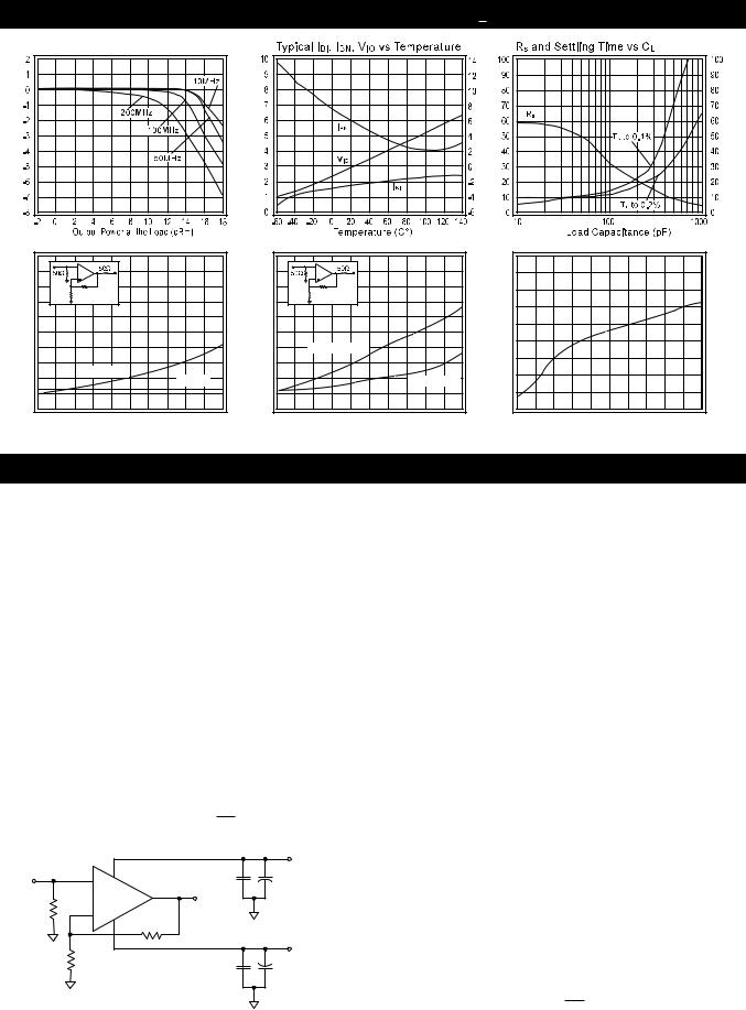
CLC449 Typical Performance Characteristics (TA = 25°C, Vcc = + 5V, Rf = 250Ω, Av = +2, RL = 100Ω) |
|
||||
(3dB/div) |
(deg) Phase |
(3dB/div) |
(deg) Phase |
(3dB/div) |
(deg) Phase |
Magnitude |
|
Magnitude |
|
Magnitude |
|
|
|
|
|
Phase (deg) |
|
|
|
|
|
|
|
|
180 |
|
|
|
|
(dBΩ) |
|
|
|
160 |
(dBc) |
|
|
|
|
|
|
|
|
|
|
||
20 log|Z| |
|
|
|
|
Distortion |
|
|
|
10k |
100k |
1M |
10M |
100M |
0.1M |
1M |
10M |
100M |
Distortion (dBc) |
|
|
|
|
Distortion (dBc) |
|
|
|
Po = 10dBm |
Intercept Point (dBm) |
Magnitude (0.1dB/div) |
(1deg/div) Phase |
Noise Voltage (nV/√Hz), Current (pA/√Hz)
3dB Bandwidth (MHz) |
D.G. (%), D.P. (deg) |
- |
|
0.1k |
1k |
10k |
100k |
1M |
10M |
100M |
|
|
Frequency (Hz) |
|
|
||
PSRR |
|
|
|
PSRR/CMRR (dB) |
|
|
|
0.1M |
1M |
10M |
100M |
(ohms) outR
Time (1ns/div) |
Time (1ns/div) |
3 |
http://www.national.com |
CLC449 Typical Performance Characteristics (TA = 25°C, Vcc = + 5V, Rf = 250Ω, Av = +2, RL = 100Ω) |
|
|||
|
Gain Compression |
|
|
|
Magnitude(1dB/div) |
(mV) |
Input |
TimeSettling(ns) |
(ohms) |
Voltage,Offset V |
BN |
|||
|
IO |
Bias |
|
R |
|
|
Current, |
|
s |
|
|
I |
|
|
|
|
BI |
|
|
|
|
I , |
|
|
|
Input |
A) ( |
|
|
Input VSWR |
Output VSWR |
Reverse Isolation (S12) |
VSWR
1.9 |
|
|
|
|
|
1.8 |
|
|
|
|
|
1.7 |
|
|
|
|
|
1.6 |
|
|
|
|
|
1.5 |
|
|
|
|
|
1.4 |
|
|
|
|
|
1.3 |
|
|
|
|
|
1.2 |
Non-Inverting |
|
|
|
|
1.1 |
|
|
|
||
|
|
|
Inverting |
|
|
1.0 |
|
|
|
|
|
0.9 |
|
|
|
|
|
0 |
100M |
200M |
300M |
400M |
500M |
|
|
Frequency (Hz) |
|
|
|
|
2.8 |
|
|
|
|
|
|
-10 |
|
2.6 |
|
|
|
|
|
|
-20 |
|
2.4 |
|
|
|
|
|
|
-30 |
|
|
|
|
|
|
|
|
|
|
2.2 |
|
|
|
|
|
|
-40 |
|
1.8 |
|
|
|
|
|
(dB)| |
|
VSWR |
2.0 |
Uncompensated |
|
|
|
|S |
-50 |
|
1.6 |
|
|
|
|||||
|
|
|
|
|
|
|
|
|
|
|
|
|
|
|
|
12 |
-60 |
|
|
|
|
|
|
|
|
|
|
1.4 |
|
|
|
|
|
|
-70 |
|
|
|
|
|
|
|
|
|
|
1.2 |
|
|
|
Compensated |
|
-80 |
|
|
|
|
|
|
|
|||
|
1.0 |
|
|
|
|
|
|
-90 |
|
0.8 |
|
|
|
|
|
-100 |
|
|
0 |
100M |
200M |
300M |
400M |
500M |
|
0 |
|
|
|
Frequency (Hz) |
|
|
|
|
|
100M |
200M |
300M |
400M |
500M |
|
Frequency (Hz) |
|
|
|
CLC449 OPERATION
CLC449 Extended Application Information
The following design and application topics will supply you with:
•A comprehensive set of design parameters and design parameter adjustment techniques.
•A set of formulas that support design parameter change prediction.
•A series of common applications that the CLC449 supports.
•A set of easy to use design guidelines for the CLC449.
Additional design applications are possible with the CLC449. If you have application questions, call 1-800-272- 9959 in the U.S. to contact a technical staff member.
DC Gain (Non-Inverting)
The non-inverting DC voltage gain for the configuration
shown in Figure 1 is:
AV = 1+ Rf Rg
|
|
|
|
|
|
Vcc |
Vin |
3 |
+ 7 |
|
0.1µF |
+ |
6.8µF |
6 |
|
|||||
|
|
CLC449 |
Vo |
|
|
|
Rt |
2 |
|
|
|
||
- |
Rf |
|
|
|
||
|
|
4 |
|
|
Vee |
|
|
|
|
|
|
|
|
|
Rg |
|
|
0.1µF |
|
6.8µF |
|
|
|
|
+ |
Figure 1: Non-Inverting Gain
The normalized gain plots in the Typical Performance Characteristics section show different feedback resistors, Rf, for different gains. These values of Rf are recommended for obtaining the highest bandwidth with minimal peaking. The resistor Rt in Figure 1 provides DC bias for the non-inverting input.
For Av ≤ 5, calculate the recommended Rf as follows:
Rf 340 - Av • Ri, where Ri = 45Ω. For Av > 5, the minimum recommended feedback resistor is Rf = 100Ω.
Select Rg to set the DC gain: Rg = |
Rf |
|
||
Av |
− 1 |
|||
|
||||
Accuracy of DC gain is usually limited by the tolerance of the external resistors Rf and Rg.
DC Gain (Unity Gain Buffer)
Unity gain buffers are easily designed with a currentfeedback amplifier as long as the recommended feedback resistor Rf = 402Ω is used and Rg = ∞, i.e. open. Parasitic capacitance at the inverting node may require a slight increase of the feedback resistor Rf to maintain a flat frequency response.
DC Gain (Inverting)
The inverting DC voltage gain for the configuration shown in Figure 2 is:
Av = − Rf
Rg
http://www.national.com |
4 |
 Loading...