


September 1999
COP884BC/COP885BC
8-Bit CMOS ROM Based Microcontrollers with 2k Memory, Comparators, and CAN Interface
General Description
The COP884BC ROM based microcontrollers are highly integrated COP8™ Feature core devices with 2k memory and advanced features including a CAN 2.0B (passive) interface and two Analog comparators. These single-chip CMOS devices are suited for applications requiring a full featured controller with a CAN interface, low EMI, and an 8-bit 39 kHz PWM timer. COP87L84BC devices are pin and software compatible 16k OTP (One Time Programmable) versions for pre-production, and for use with a range of COP8 software and hardware development tools.
Features include an 8-bit memory mapped architecture, 10 MHz CKI (crystal osc) with 1µs instruction cycle, one multifunction 16-bit timer/counter, 8-bit 39 kHz PWM timer with 2 outputs, CAN 2.0B (passive) interface, MICROWIRE/ PLUS™ serial I/O, two Analog comparators, two power saving HALT/IDLE modes, idle timer, MIWU, software selectable I/O options, Power on Reset, low EMI 4.5V to 5.5V operation, and 20/28 pin packages.
Note: A companion device with CAN interface, more I/O and memory, A/D, and USART is the COP888EB.
Devices included in this datasheet are:
Device |
Memory (bytes) |
RAM (bytes) |
I/O Pins |
Packages |
Temperature |
|
|
|
|
|
|
COP684BC |
2k ROM |
64 |
18 |
28 SOIC |
-55 to +125ÊC |
COP884BC |
2k ROM |
64 |
18 |
28 SOIC |
-40 to +85ÊC |
COP685BC |
2k ROM |
64 |
10 |
20 SOIC |
-55 to +125ÊC |
COP885BC |
2k ROM |
64 |
10 |
20 SOIC |
-40 to +85ÊC |
|
|
|
|
|
|
Key Features
nCAN 2.0B (passive) Interface
nPower On Reset (selectable)
nOne 16-bit timer, with two 16-bit registers supporting:
ÐProcessor Independent PWM mode
ÐExternal Event counter mode
ÐInput Capture mode
nHigh speed, constant resolution 8-bit PWM/frequency monitor timer with 2 output pins
n2048 bytes on-board ROM
n64 bytes on-board RAM
Additional Peripheral Features
nIdle Timer
nMulti-Input Wake Up (MIWU) with optional interrupts (7)
nTwo analog comparators
nMICROWIRE/PLUS serial I/O
I/O Features
nMemory mapped I/O
nSoftware selectable I/O options (TRI-STATE® Output, Push-Pull Output, Weak Pull-Up Input, High Impedance Input)
nSchmitt trigger inputs on ports G and L
nPackages: 28 SO with 18 I/O pins and 20 SO with 10 I/O pins
CPU/Instruction Set Features
n1 µs instruction cycle time
nEleven multi-source vectored interrupts servicing
ÐExternal Interrupt
ÐIdle Timer T0
ÐTimer T1 (with 2 Interrupts)
ÐMICROWIRE/PLUS
ÐMulti-Input Wake Up
ÐSoftware Trap
ÐPWM Timer
ÐCAN Interface (with 3 interrupts)
nVersatile and easy to use instruction set
n8-bit Stack Pointer (SP) Ð stack in RAM
nTwo 8-bit Register Indirect Data Memory Pointers (B and X)
Fully Static CMOS
nTwo power saving modes: HALT and IDLE
nLow current drain (typically <1 µA)
nSingle supply operation: 4.5V±5.5V
nTemperature ranges: −40ÊC to +85ÊC, −55ÊC to +125ÊC
Development Support
nEmulation and OTP devices
nReal time emulation and full program debug offered by MetaLink Development Systems
COP8™ , and MICROWIRE/PLUS™ are trademarks of National Semiconductor Corporation. TRI-STATE® is a registered trademark of National Semiconductor Corporation. iceMASTER® is a registered trademark of MetaLink Corporation.
Comparators, Memory, 2k with Microcontrollers Based ROM CMOS Bit-8 COP884BC/COP885BC Interface CAN and
© 1999 National Semiconductor Corporation |
DS012067 |
www.national.com |

Block Diagram
DS012067-1
FIGURE 1. Block Diagram
www.national.com |
2 |
Connection Diagrams |
Pinouts for 28-SO Package |
|
|
||||
|
|
Port |
Type |
Alt. Function |
20-Pin |
28-Pin |
|
|
|
Pin |
SO |
SO |
|||
|
|
|
|
||||
|
|
|
|
|
|
|
|
|
|
G0 |
I/O |
INTR |
17 |
25 |
|
|
|
G1 |
I/O |
|
18 |
26 |
|
|
|
G2 |
I/O |
T1B |
19 |
27 |
|
|
|
G3 |
I/O |
T1A |
20 |
28 |
|
|
|
G4 |
I/O |
SO |
1 |
1 |
|
|
|
G5 |
I/O |
SK |
2 |
2 |
|
|
|
G6 |
I |
SI |
3 |
3 |
|
|
|
G7 |
I |
CKO |
4 |
4 |
|
|
|
|
|
|
|
|
|
|
|
L0 |
I/O |
CMP1IN+/MIWU |
|
7 |
|
|
|
L1 |
I/O |
CMP1IN−/MIWU |
|
8 |
|
|
|
L2 |
I/O |
CMP10UT/MIWU |
|
9 |
|
|
|
L3 |
I/O |
CMP2IN−/MIWU |
|
10 |
|
|
|
L4 |
I/O |
CMP2IN+/MIWU |
7 |
11 |
|
DS012067-2 |
|
L5 |
I/O |
CMP2IN−/PWM1/MIWU |
8 |
12 |
|
|
L6 |
I/O |
CMP2OUT/PWM0/ |
|
13 |
||
Top View |
|
9 |
|||||
|
|
|
|
CAPTIN/MIWU |
|
||
Order Number COP884BC-xxx/WM or |
|
|
|
|
|
|
|
|
|
|
|
|
|
|
|
COP684BC-xxx/WM |
|
D0 |
O |
|
|
19 |
|
See NS Package Number M28B |
|
D1 |
O |
|
|
20 |
|
|
|
|
|
||||
|
|
D2 |
O |
|
|
21 |
|
|
|
D3 |
O |
|
|
22 |
|
|
CAN VREF |
|
|
14 |
18 |
||
|
CAN Tx0 |
O |
|
11 |
15 |
||
|
|
|
|
|
|
|
|
|
CAN Tx1 |
O |
|
10 |
14 |
||
|
CAN Rx0 |
I |
MIWU (Note 1) |
13 |
17 |
||
|
CAN Rx1 |
I |
MIWU |
12 |
16 |
||
|
|
|
|
|
|
|
|
|
|
VCC |
|
|
6 |
6 |
|
|
|
GND |
|
|
15 |
23 |
|
|
|
|
|
|
|
|
|
|
|
CKI |
I |
|
5 |
5 |
|
|
|
I |
|
16 |
24 |
||
|
|
RESET |
|
|
|||
Note 1: The MIWU function for the CAN interface is internal (see CAN inter-
DS012067-76 |
face block diagram) |
|
|
Top View |
|
Order Number COP885BC-xxx/WM or |
|
COP685BC-xxx/WM |
|
See NS Package Number M20B |
|
FIGURE 2. Connection Diagrams |
|
3 |
www.national.com |

Absolute Maximum Ratings (Note 2)
If Military/Aerospace specified devices are required, please contact the National Semiconductor Sales Office/ Distributors for availability and specifications.
Supply Voltage (VCC) |
6V |
Voltage at Any Pin |
−0.3V to V CC +0.3V |
Total Current into VCC Pin (Source) |
90 mA |
Total Current out of GND Pin (Sink) |
100 mA |
Storage Temperature Range |
−65ÊC to +150ÊC |
Note 2: Absolute maximum ratings indicate limits beyond which damage to the device may occur. DC and AC electrical specifications are not ensured when operating the device at absolute maximum ratings.
DC Electrical Characteristics COP884BC:
−40ÊC ≤ TA ≤ +85ÊC
Parameter |
Conditions |
Min |
Typ |
Max |
Units |
|
|
|
|
|
|
Operating Voltage |
|
4.5 |
|
5.5 |
V |
Power Supply Ripple (Note 3) |
Peak-to-Peak |
|
|
0.1 VCC |
V |
Supply Current |
|
|
|
|
|
CKI = 10 MHz (Note 4) |
VCC = 5.5V, tc = 1 µs |
|
|
15 |
mA |
HALT Current (Notes 5, 6) |
VCC = 5.5V, CKI = 0 MHz |
|
|
|
|
|
Power-On Reset Enabled |
|
<300 |
480 |
µA |
|
Power-On Reset Disabled |
|
<250 |
380 |
µA |
|
|
|
|
|
|
IDLE Current (Note 6) |
|
|
|
|
|
CKI = 10 MHz |
VCC = 5.5V, tc = 1 µs |
|
|
5.5 |
mA |
Input Levels (VIH, VIL) |
|
|
|
|
|
Reset, CKI |
|
|
|
|
|
Logic High |
|
0.8 VCC |
|
|
V |
Logic Low |
|
|
|
0.2 VCC |
V |
All Other Inputs |
|
|
|
|
|
Logic High |
|
0.7 VCC |
|
|
V |
Logic Low |
|
|
|
0.2 VCC |
V |
Hi-Z Input Leakage |
VCC = 5.5V |
|
|
±2 |
µA |
Input Pull-up Current |
VCC = 5.5V, VIN = 0V |
−40 |
|
−250 |
µA |
G and L Port Input Hysteresis |
(Notes 9, 10) |
|
0.05 VCC |
|
V |
Output Current Levels D Outputs |
|
|
|
|
|
Source |
VCC = 4.5V, VOH = 3.3V |
−0.4 |
|
|
mA |
Sink |
VCC = 4.5V, VOL = 1.0V |
10 |
|
|
mA |
Comparator Output (L2, L6) |
|
|
|
|
|
Source (Push-Pull) |
VCC = 4.5V, VOH = 3.3V |
−1.6 |
|
|
mA |
Sink (Push-Pull) |
VCC = 4.5V, VOL = 0.4V |
1.6 |
|
|
mA |
CAN Transmitter Outputs |
|
|
|
|
|
Source (Tx1) |
VCC = 4.5V, VOH = VCC − 0.1V |
−1.5 |
|
|
mA |
|
VCC = 4.5V, VOH = VCC − 0.6V |
−10 |
|
|
mA |
Sink (Tx0) |
VCC = 4.5V, VOL = 0.1V |
1.5 |
|
|
mA |
|
VCC = 4.5V, VOL = 0.6V |
10 |
|
|
mA |
All Others |
|
|
|
|
|
Source (Weak Pull-Up) |
VCC = 4.5V, VOH = 2.7V |
−10 |
|
−110 |
µA |
Source (Push-Pull) |
VCC = 4.5V, VOH = 3.3V |
−0.4 |
|
|
mA |
Sink (Push-Pull) |
VCC = 4.5V, VOL = 0.4V |
1.6 |
|
|
mA |
TRl-STATE Leakage |
VCC = 5.5V |
|
|
±2.0 |
µA |
Allowable Sink/Source Current per |
|
|
|
|
|
Pin |
|
|
|
|
|
D Outputs (Sink) |
|
|
|
15 |
mA |
Tx0 (Sink) (Note 10) |
|
|
|
30 |
mA |
Tx1 (Source) (Note 10) |
|
|
|
30 |
mA |
All Other |
|
|
|
3 |
mA |
|
|
|
|
|
|
www.national.com |
4 |

DC Electrical Characteristics COP884BC: (Continued)
−40ÊC ≤ TA ≤ +85ÊC
Parameter |
Conditions |
Min |
Typ |
Max |
Units |
Maximum Input Current |
|
|
|
|
|
without Latchup (Notes 8, 10) |
Room Temp |
|
|
±100 |
mA |
|
|
|
|
|
|
RAM Retention Voltage, Vr (Note 9) |
500 ns Rise and Fall Time |
2.0 |
|
|
V |
Input Capacitance |
(Note 10) |
|
|
7 |
pF |
|
|
|
|
|
|
Load Capacitance on D2 |
|
|
|
1000 |
pF |
|
|
|
|
|
|
Note 3: Maximum rate of voltage change must be less than 0.5 V/ms
Note 4: Supply current is measured after running 2000 cycles with a square wave CKI input, CKO open, inputs at VCC or GND, and outputs open.
Note 5: The HALT mode will stop CKI from oscillating in the Crystal configurations. Halt test conditions: All inputs tied to VCC; L, and G port I/Os configured as outputs and programmed low; D outputs programmed low. Parameter refers to HALT mode entered via setting bit 7 of the G Port data register. Part will pull up CKI during HALT in crystal clock mode.
Note 6: HALT and IDLE current specifications assume CAN block and comparators are disabled.
5 |
www.national.com |

Absolute Maximum Ratings (Note 7)
If Military/Aerospace specified devices are required, please contact the National Semiconductor Sales Office/ Distributors for availability and specifications.
Supply Voltage (VCC) |
7V |
Voltage at Any Pin |
−0.3V to V CC +0.3V |
Total Current into VCC Pin (Source) |
100 mA |
Total Current out of GND Pin (Sink) |
110 mA |
Storage Temperature Range |
−65ÊC to +150ÊC |
Note 7: Absolute maximum ratings indicate limits beyond which damage to the device may occur. DC and AC electrical specifications are not ensured when operating the device at absolute maximum ratings.
DC Electrical Characteristics COP684BC:
−55ÊC ≤ TA ≤ +125ÊC
|
|
Parameter |
Conditions |
Min |
Typ |
Max |
Units |
|
|
|
|
|
|
|
|
Operating Voltage |
|
4.5 |
|
5.5 |
V |
||
Power Supply Ripple (Note 3) |
Peak-to-Peak |
|
|
0.1 VCC |
V |
||
Supply Current |
|
|
|
|
|
||
CKI = 10 MHz (Note 4) |
VCC = 5.5V, tc = 1 µs |
|
|
15 |
mA |
||
HALT Current (Notes 5, 6) |
VCC = 5.5V, CKI = 0 MHz |
|
|
|
|
||
|
|
|
Power-On Reset Enabled |
|
<300 |
480 |
µA |
|
|
|
Power-On Reset Disabled |
|
<250 |
380 |
µA |
|
|
|
|
|
|
|
|
IDLE Current (Note 6) |
|
|
|
|
|
||
CKI = 10 MHz |
VCC = 5.5V, tc = 1 µs |
|
|
5.5 |
mA |
||
Input Levels (VIH, VIL) |
|
|
|
|
|
||
|
|
|
|
|
|
|
|
|
Reset, |
CKI |
|
|
|
|
|
|
Logic High |
|
0.8 VCC |
|
|
V |
|
|
Logic Low |
|
|
|
0.2 VCC |
V |
|
All Other Inputs |
|
|
|
|
|
||
|
Logic High |
|
0.7 VCC |
|
|
V |
|
|
Logic Low |
|
|
|
0.2 VCC |
V |
|
Hi-Z Input Leakage |
VCC = 5.5V |
|
|
±5 |
µA |
||
Input Pull-up Current |
VCC = 5.5V, VIN = 0V |
−35 |
|
−250 |
µA |
||
G and L Port Input Hysteresis |
(Note 9) |
|
0.05 VCC |
|
V |
||
Output Current Levels D Outputs |
|
|
|
|
|
||
|
Source |
VCC = 4.5V, VOH = 3.3V |
−0.4 |
|
|
mA |
|
|
Sink |
VCC = 4.5V, VOL = 1.0V |
9.0 |
|
|
mA |
|
Comparator Output (L2, L6) |
|
|
|
|
|
||
|
Source (Push-Pull) |
VCC = 4.5V, VOH = 3.3V |
−1.6 |
|
|
mA |
|
|
Sink (Push-Pull) |
VCC = 4.5V, VOL = 0.4V |
1.6 |
|
|
mA |
|
CAN Transmitter Outputs |
|
|
|
|
|
||
|
Source (Tx1) |
VCC = 4.5V, VOH = VCC − 0.1V |
−1.5 |
|
|
mA |
|
|
|
|
VCC = 4.5V, VOH = VCC − 0.6V |
−10 |
|
|
mA |
|
Sink (Tx0) |
VCC = 4.5V, VOL = 0.1V |
1.5 |
|
|
mA |
|
|
|
|
VCC = 4.5V, VOL = 0.6V |
10 |
|
|
mA |
All Others |
|
|
|
|
|
||
|
Source (Weak Pull-Up) |
VCC = 4.5V, VOH = 2.7V |
−9.0 |
|
−100 |
µA |
|
|
Source (Push-Pull) |
VCC = 4.5V, VOH = 3.3V |
−0.4 |
|
|
mA |
|
|
Sink (Push-Pull) |
VCC = 4.5V, VOL = 0.4V |
1.4 |
|
|
mA |
|
|
TRl-STATE Leakage |
VCC = 5.5V |
|
|
±5.0 |
µA |
|
Allowable Sink/Source Current per |
|
|
|
|
|
||
Pin |
|
|
|
|
|
||
D Outputs (Sink) |
|
|
|
12 |
mA |
||
Tx0 (Sink) (Note 10) |
|
|
|
30 |
mA |
||
Tx1 (Source) (Note 10) |
|
|
|
30 |
mA |
||
All Other |
|
|
|
2.5 |
mA |
||
|
|
|
|
|
|
|
|
www.national.com |
6 |

DC Electrical Characteristics COP684BC: (Continued)
−55ÊC £ TA £ +125ÊC
Parameter |
Conditions |
Min |
Typ |
Max |
Units |
||
Maximum Input Current |
|
|
|
|
|
||
without Latchup (Notes 8, 10) |
Room Temp |
|
|
±100 |
mA |
||
|
|
|
|
|
|
|
|
RAM Retention Voltage, Vr (Note 9) |
500 ns Rise and Fall Time |
2.0 |
|
|
V |
||
Input Capacitance |
(Note 10) |
|
|
7 |
pF |
||
|
|
|
|
|
|
|
|
Load Capacitance on D2 |
|
|
|
1000 |
pF |
||
|
|
|
|
|
|
|
|
|
|
|
|
|
|
|
|
Note 8: Pins G6 and RESET are designed with a high voltage input network. These pins allow input voltages greater than VCC and the pins will have sink current to VCC when biased at voltages greater than VCC (the pins do not have source current when biased at a voltage below VCC). The effective resistance to VCC is 750Ω (typical). These two pins will not latch up. The voltage at the pins must be limited to less than 14V.
Note 9: Condition and parameter valid only for part in HALT mode.
Note 10: Parameter characterized but not tested.
AC Electrical Characteristics COP684BC and COP884BC:
−55ÊC £ TA £ +125ÊC
Parameter |
Conditions |
Min |
Typ |
Max |
Units |
|
|
|
|
|
|
Instruction Cycle Time (tc) |
|
|
|
|
|
Crystal/Resonator |
VCC ³ 4.5V |
1.0 |
|
DC |
µs |
Inputs |
|
|
|
|
|
tSETUP |
VCC ³ 4.5V |
200 |
|
|
ns |
tHOLD |
VCC ³ 4.5V |
60 |
|
|
ns |
PWM Capture Input |
|
|
|
|
|
tSETUP |
VCC ³ 4.5V |
30 |
|
|
ns |
tHOLD |
VCC ³ 4.5V |
70 |
|
|
ns |
Output Propagation Delay |
|
|
|
|
|
(tPD1, tPD0) (Note 12) |
CL = 100 pF, RL = 2.2 kW |
|
|
|
|
SK, SO |
VCC ³ 4.5V |
|
|
0.7 |
µs |
PWM Outputs |
VCC ³ 4.5V |
|
|
75 |
ns |
All Others |
VCC ³ 4.5V |
|
|
1 |
µs |
MICROWIRE |
|
|
|
|
|
Setup Time (tUWS) (Note 13) |
|
20 |
|
|
ns |
Hold Time (tUWH) (Note 13) |
|
56 |
|
|
ns |
Output Prop Delay (tUPD) |
|
|
|
220 |
ns |
Input Pulse Width (Note 14) |
|
|
|
|
|
Interrupt High Time |
|
1 |
|
|
tc |
Interrupt Low Time |
|
1 |
|
|
tc |
Timer 1,2 High Time |
|
1 |
|
|
tc |
Timer 1,2 Low Time |
|
1 |
|
|
tc |
Reset Pulse Width (Note 13) |
|
1.0 |
|
|
µs |
|
|
|
|
|
|
Power Supply Rise Time for Proper |
|
50 µs |
|
256*tc |
|
Operation of On-Chip RESET |
|
|
|
|
|
|
|
|
|
|
|
Note 11: For device testing purposes of all AC parameters, VOH will be tested at 0.5*VCC.
Note 12: The output propagation delay is referenced to the end of the instruction cycle where the output change occurs.
Note 13: Parameter not tested.
Note 14: tc = Instruction Cycle Time.
7 |
www.national.com |
On-Chip Voltage Reference:
−55ÊC ≤ TA ≤ +125ÊC
Parameter |
Conditions |
Min |
Max |
Units |
|
|
|
|
|
Reference Voltage |
IOUT < 80 µA, |
0.5 VCC −0.12 |
0.5 V CC +0.12 |
V |
VREF |
VCC = 5V |
|
|
|
Reference Supply Current, |
IOUT = 0A, (No Load) |
|
120 |
µA |
IDD |
VCC = 5V (Note 15) |
|
|
|
Note 15: Reference supply IDD is supplied for information purposes only, it is not tested.
Comparator DC/AC Characteristics:
4.5V ≤ VCC ≤ 5.5V, −55ÊC ≤ TA ≤ +125ÊC
Parameter |
Conditions |
Min |
Typ |
Max |
Units |
|
|
|
|
|
|
Input Offset Voltage |
0.4V < VIN < VCC −1.5V |
|
±10 |
±25 |
mV |
Input Common Mode Voltage Range |
|
0.4 |
|
VCC −1.5 |
V |
Voltage Gain |
|
|
300k |
|
V/V |
Outputs Sink/Source |
See I/O-Port DC Specifications |
|
|
|
|
|
|
|
|
|
|
DC Supply Current (when enabled) |
VCC = 6.0V |
|
|
250 |
µA |
Response Time |
TBD mV Step, TBD mV Overdrive, |
|
1 |
|
µs |
|
100 pF Load |
|
|
|
|
CAN Comparator DC and AC Characteristics:
4.8V ≤ VCC ≤ 5.2V, −40ÊC ≤ TA ≤ +125ÊC
Parameters |
Conditions |
Min |
Typ |
Max |
Units |
|
|
|
|
|
|
Differential Input Voltage |
|
|
|
±25 |
mV |
|
|
|
|
|
|
Input Offset Voltage |
1.5V < VIN < VCC − 1.5V |
|
|
±10 |
mV |
Input Common Mode Voltage Range |
|
1.5 |
|
VCC − 1.5 |
V |
Input Hysteresis |
|
8 |
|
|
mV |
|
|
|
|
|
|
DS012067-4
DS012067-3
FIGURE 3. MICROWIRE/PLUS Timing Diagram
FIGURE 4. PWM/CAPTURE Timer
Input/Output Timing Diagram
www.national.com |
8 |

Typical Performance Characteristics −55ÊC ≤ TA ≤ +125ÊC
Port D Source Current |
Port D Sink Current |
DS012067-39 DS012067-40
Ports G/L Source Current Port G/L Sink Current
DS012067-41 DS012067-42
Ports G/L Weak Pull-Up Source Current Dynamic IDD vs VCC
DS012067-43 |
DS012067-44 |
9 |
www.national.com |

Typical Performance Characteristics −55ÊC ≤ TA ≤ +125ÊC (Continued)
Idle IDD vs VCC |
Halt Supply Current |
DS012067-46
|
DS012067-45 |
CAN Tx0 Sink Current |
CAN Tx1 Source Current |
DS012067-47
Pin Descriptions
VCC and GND are the power supply pins.
CKI is the clock input. The clock can come from a crystal oscillator (in conjunction with CKO). See Oscillator Description section.
RESET is the master reset input. See Reset Description section.
The device contains one bidirectional 8-bit I/O port (G), and one 7-bit bidirectional I/O port (L) where each individual bit may be independently configured as an input (Schmitt trigger inputs on ports G and L), output or TRI-STATE® under program control. Three data memory address locations are allocated for each of these I/O ports. Each I/O port has two associated 8-bit memory mapped registers, the CONFIGURATION register and the output DATA register. A memory mapped address is also reserved for the input pins of each I/O port. (See the memory map for the various addresses associated with the I/O ports.) Figure 5 shows the I/O port configurations for the device. The DATA and CONFIGURATION registers allow for each port bit to be individually configured under software control as shown below:
|
|
DS012067-48 |
|
|
|
|
|
Configuration |
Data |
Port Set-Up |
|
Register |
Register |
||
|
|||
|
|
|
|
0 |
0 |
Hi-Z Input (TRI-STATE |
|
|
|
Output) |
|
0 |
1 |
Input with Weak Pull-Up |
|
1 |
0 |
Push-Pull Zero Output |
|
1 |
1 |
Push-Pull One Output |
|
|
|
|
PORT L is a 7-bit I/O port. All L-pins have Schmitt triggers on the inputs.
Port L supports Multi-Input Wake Up (MIWU) on all seven pins.
Port L has the following alternate features:
L6 MIWU or CMP2OUT or PWM0 or CAPTIN
L5 MIWU or CMP2IN− or PWM1
L4 MIWU or CMP2IN+
L3 MIWU or CMP2IN−
L2 MIWU or CMP1OUT
L1 MIWU or CMP1IN−
L0 MIWU or CMP1IN+
Port G is an 8-bit port with 5 I/O pins (G0±G5), an input pin (G6), and one dedicated output pin (G7). Pins G0±G6 all have Schmitt Triggers on their inputs. G7 serves as the dedicated output pin for the CKO clock output. There are two reg-
www.national.com |
10 |
Pin Descriptions (Continued)
isters associated with the G Port, a data register and a configuration register. Therefore, each of the 6 I/O bits (G0±G5) can be individually configured under software control.
Since G6 is an input only pin and G7 is the dedicated CKO clock output pin the associated bits in the data and configuration registers for G6 and G7 are used for special purpose functions as outlined below. Reading the G6 and G7 data bits will return zeroes.
Note that the chip will be placed in the HALT mode by writing a ª1º to bit 7 of the Port G Data Register. Similarly the chip will be placed in the IDLE mode by writing a ª1º to bit 6 of the Port G Data Register.
Writing a ª1º to bit 6 of the Port G Configuration Register enables the MICROWIRE/PLUS to operate with the alternate phase of the SK clock.
|
Config. Register |
Data Register |
|
|
|
G7 |
|
HALT |
|
|
|
G6 |
Alternate SK |
IDLE |
|
|
|
CAN pins: For the on-chip CAN interface this device has five dedicated pins with the following features:
VREF |
On-chip reference voltage with the value of VCC/2 |
Rx0 |
CAN receive data input pin. |
Rx1 |
CAN receive data input pin. |
Tx0 |
CAN transmit data output pin. This pin may be put in |
|
the TRI-STATE mode with the TXEN0 bit in the CAN |
|
Bus control register. |
Tx1 |
CAN transmit data output pin. This pin may be put in |
|
the TRI-STATE mode with the TXEN1 bit in the CAN |
|
Bus control register. |
Port G has the following alternate features:
G6 SI (MICROWIRE Serial Data Input)
G5 SK (MICROWIRE Serial Clock)
G4 SO (MICROWIRE Serial Data Output)
G3 T1A (Timer T1 I/O)
G2 T1B (Timer T1 Capture Input)
G0 INTR (External Interrupt Input)
Port G has the following dedicated function:
G7 CKO Oscillator dedicated output
Port D is a 4-bit output port that is preset high when RESET goes low. The user can tie two or more D port outputs (except D2) together in order to get a higher drive.
Note: Care must be exercised with the D2 pin operation. At RESET, the external loads on this pin must ensure that the output voltages stay above 0.8 VCC to prevent the chip from entering special modes. Also keep the external loading on D2 to less than 1000 pF.
DS012067-5
FIGURE 5. I/O Port Configurations
Functional Description
The architecture of the device utilizes a modified Harvard architecture. With the Harvard architecture, the control store program memory (ROM) is separated from the data store memory (RAM). Both ROM and RAM have their own separate addressing space with separate address buses. The architecture, though based on Harvard architecture, permits transfer of data from ROM to RAM.
CPU REGISTERS
The CPU can do an 8-bit addition, subtraction, logical or shift operation in one instruction (tc) cycle time.
There are five CPU registers:
A is the 8-bit Accumulator Register
PC is the 15-bit Program Counter Register
PU is the upper 7 bits of the program counter (PC)
PL is the lower 8 bits of the program counter (PC)
B is an 8-bit RAM address pointer, which can be optionally post auto incremented or decremented.
X is an 8-bit alternate RAM address pointer, which can be optionally post auto incremented or decremented.
SP is the 8-bit stack pointer, which points to the subroutine/ interrupt stack (in RAM). The SP is initialized to RAM address 02F with reset.
All the CPU registers are memory mapped with the exception of the Accumulator (A) and the Program Counter (PC).
PROGRAM MEMORY
Program memory for the device consists of 2048 bytes of ROM. These bytes may hold program instructions or constant data (data tables tor the LAID instruction, jump vectors for the JID instruction, and interrupt vectors for the VIS instruction). The program memory is addressed by the 15-bit program counter (PC). All interrupts in the device vector to program memory location 0FF Hex.
DATA MEMORY
The data memory address space includes the on-chip RAM and data registers, the I/O registers (Configuration, Data and Pin), the control registers, the MICROWIRE/PLUS SIO shift register, and the various registers, and counters associated with the timers (with the exception of the IDLE timer). Data memory is addressed directly by the instruction or indirectly by the B, X and SP pointers.
11 |
www.national.com |

Functional Description (Continued)
The device has 64 bytes of RAM. Sixteen bytes of RAM are mapped as ªregistersº at addresses 0F0 to 0FF Hex. These registers can be loaded immediately, and also decremented and tested with the DRSZ (decrement register and skip if zero) instruction. The memory pointer registers X, SP, and B are memory mapped into this space at address locations 0FC to 0FE Hex respectively, with the other registers (other than reserved register 0FF) being available for general usage.
The instruction set permits any bit in memory to be set, reset or tested. All I/O and registers (except A and PC) are memory mapped; therefore, I/O bits and register bits can be directly and individually set, reset and tested. The accumulator (A) bits can also be directly and individually tested.
Note: RAM contents are undefined upon power-up.
RESET
The RESET input when pulled low initializes the microcontroller. lnitialization will occur whenever the RESET input is pulled low. Upon initialization, the data and configuration registers for Ports L and G, are cleared, resulting in these Ports being initialized to the TRI-STATE mode. Port D is initialized high with RESET. The PC, PSW, CNTRL, and ICNTRL control registers are cleared. The Multi-Input Wake Up registers WKEN, WKEDG, and WKPND are cleared. The Stack Pointer, SP, is initialized to 02F Hex.
The following initializations occur with RESET:
Port L: TRI-STATE
Port G: TRI-STATE
Port D: HIGH
PC: CLEARED
PSW, CNTRL and ICNTRL registers: CLEARED
Accumulator and Timer 1:
RANDOM after RESET with power already applied
RANDOM after RESET at power-on
SP (Stack Pointer): Loaded with 2F Hex
CMPSL (Comparator control register): CLEARED
PWMCON (PWM control register): CLEARED
B and X Pointers:
UNAFFECTED after RESET with power already applied
RANDOM after RESET at power-up
RAM:
UNAFFECTED after RESET with power already applied
RANDOM after RESET at power-up
CAN:
The CAN Interface comes out of external reset in the ªerror-activeº state and waits until the user's software sets either one or both of the TXEN0, TXEN1 bits to ª1º. After that, the device will not start transmission or reception of a frame until eleven consecutive ªrecessiveº (undriven) bits have been received. This is done to ensure that the output drivers are not enabled during an active message on the bus.
CSCAL, CTlM, TCNTL, TEC, REC: CLEARED
RTSTAT: CLEARED with the exception of the TBE bit which is set to 1
RID, RIDL, TID, TDLC: RANDOM
ON-CHIP POWER-ON RESET
The device is designed with an on-chip power-on reset circuit which will trigger a 256 tc delay as VCC rises above the minimum RAM retention voltage (Vr). This delay allows the oscillator to stabilize before the device exits the reset state. The contents of data registers and RAM are unknown following an on-chip power-on reset. The external reset takes priority over the on-chip reset and will deactivate the 256 tc delay if in progress.
When using external reset, the external RC network shown in Figure 6 should be used to ensure that the RESET pin is held low until the power supply to the chip stabilizes.
Under no circumstances should the RESET pin be allowed to float. If the on-chip power-on reset feature is being used, RESET should be connected directly to VCC. Be aware of the Power Supply Rise Time requirements specified in the DC Specifications Table. These requirements must be met for the on-chip power-on reset to function properly.
The on-chip power-on reset circuit may reset the device if the operating voltage (VCC) goes below Vr.
DS012067-6
RC > 5 x Power Supply Rise Time
FIGURE 6. Recommended Reset Circuit
Oscillator Circuits
The chip can be driven by a clock input on the CKI input pin which can be between DC and 10 MHz. The CKO output clock is on pin G7. The CKI input frequency is divided by 10 to produce the instruction cycle clock (1/tc).
Figure 7 shows the Crystal diagram.
DS012067-7
FIGURE 7. Crystal Oscillator Diagram
CRYSTAL OSCILLATOR
CKI and CKO can be connected to make a closed loop crystal (or resonator) controlled oscillator.
Table 1 shows the component values required for various standard crystal values.
www.national.com |
12 |
Oscillator Circuits (Continued)
TABLE 1. Crystal Oscillator Configuration, TA = 25ÊC
R1 |
R2 |
C1 |
C2 |
CKI Freq. |
Conditions |
|||||
(kΩ) |
(MΩ) |
(pF) |
(pF) |
(MHz) |
||||||
|
|
|||||||||
0 |
1 |
30 |
30±36 |
10 |
|
VCC = 5V |
||||
0 |
1 |
30 |
30±36 |
4 |
|
VCC = 5V |
||||
0 |
1 |
200 |
100±150 |
0.455 |
|
VCC = 5V |
||||
Control Registers |
|
|
|
|
|
|||||
CNTRL Register (Address X©00EE) |
|
|
||||||||
|
|
|
|
|
|
|
|
|
||
T1C3 |
T1C2 |
T1C1 |
T1C0 |
MSEL |
IEDG |
|
SL1 |
SL0 |
||
|
|
|
|
|
|
|
|
|
|
|
Bit 7 |
|
|
|
|
|
|
|
|
Bit 0 |
|
|
|
|
|
|
|
|
|
|
|
|
The Timer1 (T1) and MICROWIRE/PLUS control register contains the following bits:
T1C3 |
Timer T1 mode control bit |
T1C2 |
Timer T1 mode control bit |
T1C1 |
Timer T1 mode control bit |
T1C0 |
Timer T1 Start/Stop control in timer |
|
modes 1 and 2, T1 Underflow Interrupt |
|
Pending Flag in timer mode 3 |
MSEL |
Selects G5 and G4 as MICROWIRE/PLUS |
|
signals SK and SO respectively |
IEDG |
External interrupt edge polarity select |
|
(0 = Rising edge, 1 = Falling edge) |
SL1 & SL0 |
Select the MICROWIRE/PLUS clock divide |
|
by (00 = 2, 01 = 4, 1x = 8) |
PSW Register (Address X©00EF)
HC |
C |
T1PNDA |
T1ENA |
EXPND |
BUSY |
EXEN |
GIE |
|
|
|
|
|
|
|
|
Bit 7 |
|
|
|
|
|
|
Bit 0 |
|
|
|
|
|
|
|
|
The PSW register contains the following select bits:
HC |
Half Carry Flag |
C |
Carry Flag |
T1PNDA Timer T1 Interrupt Pending Flag (Autoreload RA in mode 1, T1 Underflow in Mode 2, T1A capture edge in mode 3)
T1ENA |
Timer T1 Interrupt Enable for Timer Underflow |
|
or T1A Input capture edge |
EXPND |
External interrupt pending |
BUSY |
MICROWIRE/PLUS busy shifting flag |
EXEN |
Enable external interrupt |
GIE |
Global interrupt enable (enables interrupts) |
The Half-Carry flag is also affected by all the instructions that affect the Carry flag. The SC (Set Carry) and R/C (Reset Carry) instructions will respectively set or clear both the carry flags. In addition to the SC and R/C instructions, ADC, SUBC, RRC and RLC instructions affect the Carry and Half Carry flags.
ICNTRL Register (Address X©00E8)
Reserved |
LPEN |
|
T0PND |
T0EN |
µWPND |
µWEN |
T1PNDB |
T1ENB |
|
|
|
|
|
|
|
|
|
Bit 7 |
|
|
|
|
|
|
Bit 0 |
|
|
|
|
|
|
|
|
|
|
The ICNTRL register contains the following bits: |
||||||||
Reserved |
This bit is reserved and should be zero. |
|||||||
LPEN |
L Port Interrupt Enable (Multi-Input Wakeup/ |
|||||||
|
|
Interrupt) |
||||||
T0PND |
Timer T0 |
Interrupt pending |
T0EN |
Timer T0 |
Interrupt Enable (Bit 12 toggle) |
µWPND |
MICROWIRE/PLUS interrupt pending |
|
µWEN |
Enable MICROWIRE/PLUS interrupt |
|
T1PNDB |
Timer T1 Interrupt Pending Flag for T1B cap- |
|
|
ture edge |
|
T1ENB |
Timer T1 Interrupt Enable for T1B Input cap- |
|
|
ture edge |
|
Timers
The device contains a very versatile set of timers (T0, T1, and an 8-bit PWM timer). All timers and associated autoreload/capture registers power up containing random data.
Figure 8 shows a block diagram for timers T1 and T0 on the device.
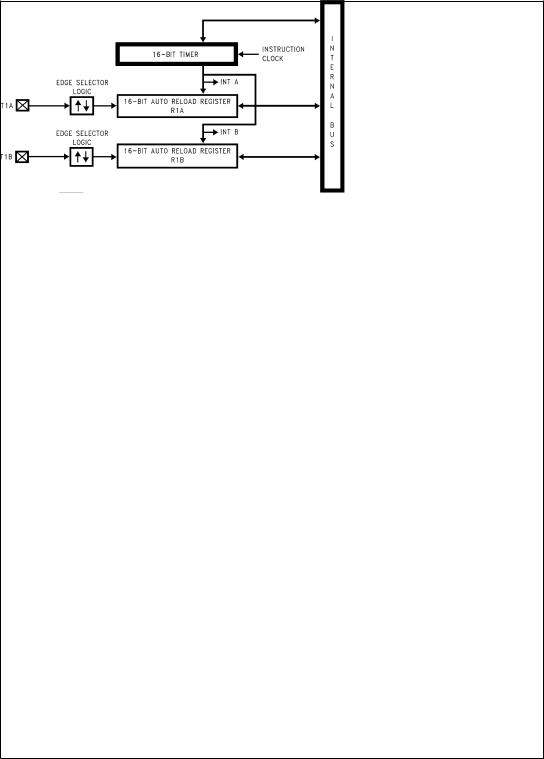
DS012067-8
FIGURE 8. Timers T1 and T0
TIMER T0 (IDLE TIMER)
The device supports applications that require maintaining real time and low power with the IDLE mode. This IDLE mode support is furnished by the IDLE timer T0, which is a 16-bit timer. The Timer T0 runs continuously at the fixed rate of the instruction cycle clock, tc. The user cannot read or write to the IDLE Timer T0, which is a count down timer.
The Timer T0 supports the following functions:
Exit out of the Idle Mode (See Idle Mode description)
Start up delay out of the HALT mode
The IDLE Timer T0 can generate an interrupt when the thirteenth bit toggles. This toggle is latched into the T0PND pending flag, and will occur every 4.096 ms at the maximum clock frequency (tc = 1 µs). A control flag T0EN allows the interrupt from the thirteenth bit of Timer T0 to be enabled or disabled. Setting T0EN will enable the interrupt, while resetting it will disable the interrupt.
TIMER T1
The device has a powerful timer/counter block, T1.
The timer block consists of a 16-bit timer, T1, and two supporting 16-bit autoreload/capture registers, R1A and R1B. The timer block has two pins associated with it, T1A and T1B. The pin T1A supports I/O required by the timer block, while the pin T1B is an input to the timer block. The powerful and flexible timer block allows the device to easily perform all timer functions with minimal software overhead. The timer
13 |
www.national.com |
Timers (Continued)
block has three operating modes: Processor Independent PWM mode, External Event Counter mode, and Input Capture mode.
The control bits T1C3, T1C2, and T1C1 allow selection of the different modes of operation.
Mode 1. Processor Independent PWM Mode
As the name suggests, this mode allows the device to generate a PWM signal with very minimal user intervention.
The user only has to define the parameters of the PWM signal (ON time and OFF time). Once begun, the timer block will continuously generate the PWM signal completely independent of the microcontroller. The user software services the timer block only when the PWM parameters require updating.
In this mode the timer T1 counts down at a fixed rate of tc. Upon every underflow the timer is alternately reloaded with the contents of supporting registers, R1A and R1B. The very first underflow of the timer causes the timer to reload from the register R1A. Subsequent underflows cause the timer to be reloaded from the registers alternately beginning with the register R1B.
The T1 Timer control bits, T1C3, T1C2 and T1C1 set up the timer for PWM mode operation.
Figure 9 shows a block diagram of the timer in PWM mode. The underflows can be programmed to toggle the T1A output pin. The underflows can also be programmed to generate interrupts.
DS012067-9
FIGURE 9. Timer 1 in PWM MODE
Underflows from the timer are alternately latched into two pending flags, T1PNDA and T1PNDB. The user must reset these pending flags under software control. Two control enable flags, T1ENA and T1ENB, allow the interrupts from the timer underflow to be enabled or disabled. Setting the timer enable flag T1ENA will cause an interrupt when a timer underflow causes the R1A register to be reloaded into the timer. Setting the timer enable flag T1ENB will cause an interrupt when a timer underflow causes the R1B register to be reloaded into the timer. Resetting the timer enable flags will disable the associated interrupts.
Either or both of the timer underflow interrupts may be enabled. This gives the user the flexibility of interrupting once per PWM period on either the rising or falling edge of the PWM output. Alternatively, the user may choose to interrupt on both edges of the PWM output.
Mode 2. External Event Counter Mode
This mode is quite similar to the processor independent PWM mode described above. The main difference is that the timer, T1, is clocked by the input signal from the T1A pin. The T1 timer control bits, T1C3, T1C2 and T1C1 allow the timer to be clocked either on a positive or negative edge from the T1A pin. Underflows from the timer are latched into the T1PNDA pending flag. Setting the T1ENA control flag will cause an interrupt when the timer underflows.
In this mode the input pin T1B can be used as an independent positive edge sensitive interrupt input if the T1ENB control flag is set. The occurrence of a positive edge on the T1B input pin is latched into the T1PNDB flag.
Figure 10 shows a block diagram of the timer in External Event Counter mode.
Note: The PWM output is not available in this mode since the T1A pin is being used as the counter input clock.
Mode 3. Input Capture Mode
The device can precisely measure external frequencies or time external events by placing the timer block, T1, in the input capture mode.
In this mode, the timer T1 is constantly running at the fixed tc rate. The two registers, R1A and R1B, act as capture registers. Each register acts in conjunction with a pin. The register R1A acts in conjunction with the T1A pin and the register R1B acts in conjunction with the T1B pin.
The timer value gets copied over into the register when a trigger event occurs on its corresponding pin. Control bits, T1C3, T1C2 and T1C1, allow the trigger events to be specified either as a positive or a negative edge. The trigger condition for each input pin can be specified independently.
The trigger conditions can also be programmed to generate interrupts. The occurrence of the specified trigger condition on the T1A and T1B pins will be respectively latched into the pending flags, T1PNDA and T1PNDB. The control flag T1ENA allows the interrupt on T1A to be either enabled or disabled. Setting the T1ENA flag enables interrupts to be generated when the selected trigger condition occurs on the T1A pin. Similarly, the flag T1ENB controls the interrupts from the T1B pin.
Underflows from the timer can also be programmed to generate interrupts. Underflows are latched into the timer T1C0 pending flag (the T1C0 control bit serves as the timer underflow interrupt pending flag in the Input Capture mode). Consequently, the T1C0 control bit should be reset when entering the Input Capture mode. The timer underflow interrupt is enabled with the T1ENA control flag. When a T1A interrupt occurs in the Input Capture mode, the user must check both the T1PNDA and T1C0 pending flags in order to determine whether a T1A input capture or a timer underflow (or both) caused the interrupt.
Figure 11 shows a block diagram of the timer in Input Capture mode.
www.national.com |
14 |
Timers (Continued)
DS012067-10
FIGURE 10. Timer 1 in External Event Counter Mode
DS012067-11
FIGURE 11. Timer 1 in Input Capture Mode
15 |
www.national.com |

Timers (Continued)
TIMER CONTROL FLAGS
The control bits and their functions are summarized below.
T1C3 Timer mode control
T1C2 Timer mode control
T1C1 Timer mode control
T1C0 Timer Start/Stop control in Modes 1 and 2 (Processor Independent PWM and External Event Counter), where 1 = Start, 0 = Stop
Timer Underflow Interrupt Pending Flag in Mode 3 (Input Capture)
T1PNDA Timer Interrupt Pending Flag
T1ENA Timer Interrupt Enable Flag
1 = Timer Interrupt Enabled
0 = Timer Interrupt Disabled
T1PNDB Timer Interrupt Pending Flag
T1ENB Timer Interrupt Enable Flag
1 = Timer Interrupt Enabled
0 = Timer Interrupt Disabled
The timer mode control bits (T1C3, T1C2 and T1C1) are detailed below:
Mode |
T1C3 |
T1C2 |
T1C1 |
Description |
Interrupt A |
Interrupt B |
Timer |
|
Source |
Source |
Counts On |
||||||
|
|
|
|
|
||||
|
|
|
|
|
|
|
|
|
|
1 |
0 |
1 |
PWM: T1A Toggle |
Autoreload RA |
Autoreload RB |
tC |
|
1 |
1 |
0 |
0 |
PWM: No T1A |
Autoreload RA |
Autoreload RB |
tC |
|
|
|
|
|
Toggle |
|
|
||
|
|
|
|
|
|
|
||
|
|
|
|
|
|
|
|
|
|
0 |
0 |
0 |
External Event |
Timer |
Pos. T1B Edge |
Pos. T1A |
|
2 |
|
|
|
Counter |
Underflow |
|
Edge |
|
|
|
|
|
|
|
|
||
0 |
0 |
1 |
External Event |
Timer |
Pos. T1B Edge |
Pos. T1A |
||
|
||||||||
|
|
|
|
Counter |
Underflow |
|
Edge |
|
|
|
|
|
|
|
|
|
|
|
0 |
1 |
0 |
Captures: |
Pos. T1A Edge |
Pos. T1B Edge |
tC |
|
|
|
|
|
T1A Pos. Edge |
or Timer |
|
|
|
|
|
|
|
T1B Pos. Edge |
Underflow |
|
|
|
|
|
|
|
|
|
|
|
|
|
1 |
1 |
0 |
Captures: |
Pos. T1A |
Neg. T1B |
tC |
|
|
|
|
|
T1A Pos. Edge |
Edge or Timer |
Edge |
|
|
3 |
|
|
|
T1B Neg. Edge |
Underflow |
|
|
|
|
|
|
|
|
|
|
||
0 |
1 |
1 |
Captures: |
Neg. T1A |
Neg. T1B |
tC |
||
|
||||||||
|
|
|
|
T1A Neg. Edge |
Edge or Timer |
Edge |
|
|
|
|
|
|
T1B Neg. Edge |
Underflow |
|
|
|
|
|
|
|
|
|
|
|
|
|
1 |
1 |
1 |
Captures: |
Neg. T1A |
Neg. T1B |
tC |
|
|
|
|
|
T1A Neg. Edge |
Edge or Timer |
Edge |
|
|
|
|
|
|
T1B Neg. Edge |
Underflow |
|
|
|
|
|
|
|
|
|
|
|
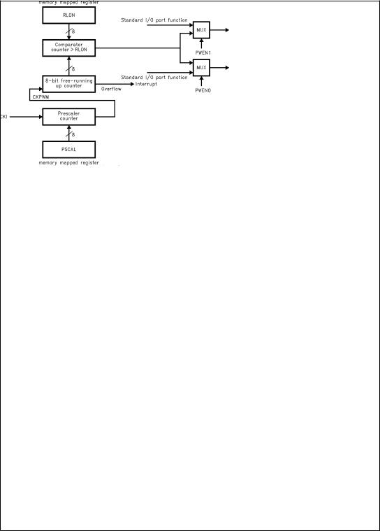
HIGH SPEED, CONSTANT RESOLUTION
PWM TIMER
The device has one processor independent PWM timer. The PWM timer operates in two modes: PWM mode and capture mode. In PWM mode the timer outputs can be programmed to two pins PWM0 and PWM1. In capture mode, pin PWM0 functions as the capture input. Figure 12 shows a block diagram for this timer in capture mode and Figure 13 shows a block diagram for the timer in PWM mode.
PWM Timer Registers
The PWM Timer has three registers: PWMCON, the PWM control register, RLON, the PWM on-time register and PSCAL, the prescaler register.
PWM Prescaler Register (PSCAL) (Address X'00A0)
The prescaler is the clock source for the counter in both PWM mode and in frequency monitor mode.
PSCAL is a read/write register that can be used to program the prescaler. The clock source to the timer in both PWM and capture modes can be programmed to CKI/N where N =
PSCAL + 1, so the maximum PWM clock frequency = CKI and the minimum PWM clock frequency = CKI/256. The processor is able to modify the PSCAL register regardless of whether the counter is running or not and the change in frequency occurs with the next underflow of the prescaler (CKPWM).
PWM On-time Register (RLON) (Address X'00A1)
RLON is a read/write register. In PWM mode the timer output will be a ª1º for RLON counts out of a total cycle of 255 PWM clocks. In capture mode it is used to program the threshold frequency.
The PWM timer is specially designed to have a resolution of 255 PWM clocks. This allows the duty cycle of the PWM output to be selected between 1/255 and 254/255. A value of 0 in the RLON register will result in the PWM output being continuously low and a value of 255 will result in the PWM output being continuously high.
Note: The effect of changing the RLON register during active PWM mode operation is delayed until the boundary of a PWM cycle. In capture mode the effect takes place immediately.
www.national.com |
16 |
Timers (Continued)
DS012067-12
FIGURE 12. PWM Timer Capture Mode Block Diagram
|
DS012067-13 |
FIGURE 13. PWM Timer PWM Mode Block Diagram |
|
PWM Control Register (PWMCON) (Address X'00A2) |
PWEN1 Enable PWM1 output function on I/O port. |
Reserved |
ESEL |
PWPND |
PWIE |
PWMD |
PWON |
PWEN1 |
PWEN0 |
|
|
|
|
|
|
|
|
Bit 7 |
|
|
|
|
|
|
Bit 0 |
|
|
|
|
|
|
|
|
Note: The associated bits in the configuration and data register of the I/O- port have to be setup as outputs and/or inputs in addition to setting the PWEN bits.
The PWMCON Register Bits are:
Reserved |
This bit is reserved and must be zero. |
ESEL |
Edge select bit, ª1º for falling edge, ª0º for rising |
|
edge. |
PWPND |
PWM interrupt pending bit. |
PWIE |
PWM interrupt enable bit. |
PWMD |
PWM Mode bit, ª1º for PWM mode, ª0º for fre- |
|
quency monitor mode. |
PWON |
PWM start Bit, ª1º to start timer, ª0º to stop timer. |
PWEN0 Enable PWM0 output/input function on I/O port.
PWM Mode
The PWM timer can generate PWM signals at frequencies up to 39 kHz (@ tc = 1 µs) with a resolution of 255 parts. Lower PWM frequencies can be programmed via the prescaler.
If the PWM mode bit (PWMD) in the PWM configuration register (PWMCON) is set to ª1º the timer operates in PWM mode. In this mode, the timer generates a PWM signal with
17 |
www.national.com |
Timers (Continued)
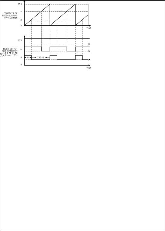
a fixed, non-programmable repetition rate of 255 PWM clock cycles. The timer is clocked by the output of an 8-bit, programmable prescaler, which is clocked with the chip's CKI frequency. Thus the PWM signal frequency can be calculated with the formula:
Selecting the PWM mode by setting PWMD to ª1º, but not yet starting the timer (PWON is ª0º), will set the timer output to ª1º.
The contents of an 8-bit register, RLON, multiplied by the clock cycle of the prescaler output defines the time between overflow (or starting) and the falling edge of the PWM output.
Once the timer is started, the timer output goes low after RLON cycles and high after a total of 255 cycles. The procedure is continually repeated. In PWM mode the timer is available at pins PWM0 and/or PWM1, provided the port configuration bits for those pins are defined as outputs and the PWEN0 and/or PWEN1 bits in the PWMCON register are set.
The PWM timer is started by the software setting the PWON bit to ª1º. Starting the timer initializes the timer register. From this point, the timer will continually generate the PWM signal, independent of any processor activity, until the timer is stopped by software setting the PWON bit to ª0º. The processor is able to modify the RLON register regardless of whether the timer is running. If RLON is changed while the timer is running, the previous value of RLON is used for comparison until the next overflow occurs, when the new value of RLON is latched into the comparator inputs.
When the timer overflows, the PWM pending flag (PWPND) is set to ª1º. If the PWM interrupt enable bit (PWIE) is also set to ª1º, timer overflow will generate an interrupt. The PWPND bit remains set until the user's software writes a ª0º to it. If the software writes a ª1º to the PWPND bit, this has no effect. If the software writes a ª0º to the PWPND bit at the same time as the hardware writes to the bit, the hardware has precedence.
Note: The software controlling the duty cycle is able to change the PWM duty cycle without having to wait for the timer overflow.
Figure 14 shows how the PWM output is implemented. The PWM Timer output is set to ª1º on an overflow of the timer and set to ª0º when the timer is greater than RLON. The output can be multiplexed to two pins.
Capture Mode
If the PWM mode bit (PWMD) is set to ª0º the PWM Timer operates in capture mode. Capture mode allows the programmer to test whether the frequency of an external source exceeds a certain threshold.
If PWMD is ª0º and PWON is ª0º, the timer output is set to ª0º. In capture mode the timer output is available at pin PWM1, provided the port configuration register bit for that pin is set up as an output and the PWEN1 bit in the PWMCON register is set. Setting PWON to ª1º will initialize the timer register and start the counter. A rising edge, or if selected, a falling edge, on the FMONIN input pin will initialize the timer register and clear the timer output. The counter continues to count up after being initialized. The ESEL bit determines whether the active edge is a rising or a falling edge.
DS012067-14
FIGURE 14. PWM Mode Operation
If, in capture mode PWM0 is configured incorrectly as an output and is enabled via the PWEN0 bit, the timer output will feedback into the PWM block as the timer input.
The contents of the counter are continually compared with the RLON register. If the frequency of the input edges is sufficiently high, the contents of the counter will always be less
than the value in RLON. However, if the frequency of the input edges is too low, the free-running counter value will count up beyond the value in RLON.
When the counter is greater than RLON, the PWM timer output is set to ª1º. It is set to ª0º by a detected edge on the timer input or when the counter overflows. When the counter be-
www.national.com |
18 |
 Loading...