


CLC440MDC
NSC CLC440MDC, CLC440AJP, CLC440AJE-TR13, CLC440AJE, CLC440AJ Datasheet
...
Frequency Response (A
V
= +2V/V)
Features
■
Unity-gain stable
■
High unity-gain bandwidth: 750MHz
■
Ultra-low differential gain:0.015%
■
Very low differential phase: 0.025°
■
Low power: 70mW
■
Extremely fast slew rate:1500V/µs
■
High output current: 90mA
■
Low noise: 3.5nV/√Hz
■
Dual ±2.5V to ±6V or single 5V to 12V supplies
Applications
■
Professional video
■
Graphics workstations
■
Test equipment
■
Video switching & routing
■
Communications
■
Medical imaging
■
A/D drivers
■
Photo diode transimpedance amplifiers
■
Improved replacement f or CLC420 or OPA620
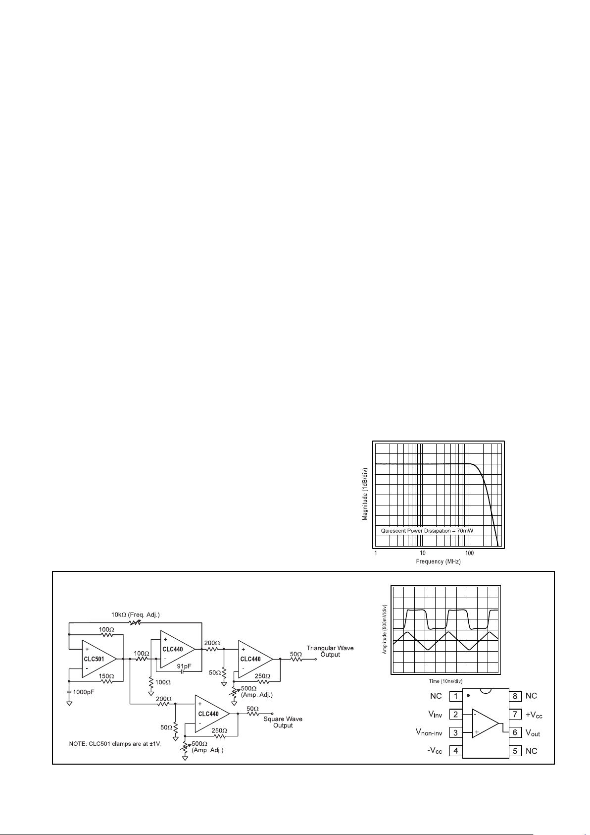
Typical Application
10MHz to 40MHz Square and Triangular Wave Generator
Pinout
DIP & SOIC
General Description
The CLC440 is a wideband, low-power, voltage feedback op amp
that offers 750MHz unity-gain bandwidth, 1500V/µs slew rate, and
90mA output current. For video applications, the CLC440 sets new
standards for voltage f eedback monolithics b y off ering the impres-
sive combination of 0.015% differential gain and 0.025° differen-
tial phase errors while dissipating a mere 70mW.
The CLC440 incorporates the proven properties of Comlinear’s
current feedback amplifiers (high bandwidth, f ast sle wing, etc.) into a
“classical” voltage feedback architecture. This amplifier possesses
truly differential and fully symmetrical inputs both having a high
900kΩ impedance with matched low input bias currents.
Furthermore, since the CLC440 incorporates voltage feedback, a
specific R
f
is not required for stability. This flexibility in choosing R
f
allows for numerous applications in wideband filtering and integration.
Unlike several other high-speed voltage feedback op amps, the
CLC440 operates with a wide range of dual or single supplies
allowing for use in a multitude of applications with limited supply
availability. The CLC440’s low 3.5nV/√Hz(e
n
) and 2.5pA/√Hz(i
n
)
noise sets a very low noise floor.
CLC440
High-Speed, Low-Power,Voltage Feedback Op Amp
N
June 1999
CLC440
High-Speed, Low-Power, Voltage Feedback Op Amp
Generator Waveforms
© 1999 National Semiconductor Corporation http://www.national.com
Printed in the U.S.A.

PARAMETERS CONDITIONS TYP MIN/MAX RATINGS UNITS NOTES
Ambient T emper ature CLC440 +25˚C +25˚C 0 to 70˚C -40 to 85˚C
FREQUENCY DOMAIN RESPONSE
-3dB bandwidth A
V
=+2 V
out
< 0.2V
pp
260 165 165 135 MHz
V
out
< 4.0V
pp
190 150 135 130 MHz
-3dB bandwidth A
V
=+1 V
out
< 0.2V
pp
750 MHz
gain bandwidth product V
out
< 0.2V
pp
230 MHz
gain flatness
V
out
< 2.0V
pp
DC to 75MHz
0.05 0.15 0.20 0.20 dB
linear phase deviation
V
out
< 2.0V
pp
DC to 75MHz
0.8 1.2 1.5 1.5 deg
differential gain 4.43MHz, R
L
=150Ω 0.015 0.03 0.04 0.04 %
differential phase 4.43MHz, R
L
=150Ω 0.025 0.05 0.06 0.06 deg
TIME DOMAIN RESPONSE
rise and fall time 2V step 1.5 2.0 2.2 2.5 ns
4V step 3.2 4.2 4.5 5.0 ns
settling time to 0.05% 2V step 10 14 16 16 ns
overshoot 4V step 7 13 13 13 %
slew rate 4V step, ±0.5V crossing 1500 900 750 600 V/µs
DISTORTION AND NOISE RESPONSE
2nd harmonic distortion 2V
pp
, 5MHz -64 -59 -59 -59 dBc
2V
pp
, 20MHz -52 -46 -46 -46 dBc
3rd harmonic distortion 2V
pp
, 5MHz -70 -65 -64 -64 dBc
2V
pp
, 20MHz -51 -45 -43 -43 dBc
equivalent input noise
voltage >1MHz 3.5 4.5 5.0 5.0 nV/√Hz
current >1MHz 2.5 3.5 4.0 4.0 pA/√Hz
STATIC DC PERFORMANCE
input offset voltage 1.0 3.0 3.5 4.0 mV A
average drift 5.0 10 10 µV/°C
input bias current 10 30 35 40 µAA
average drift 30 50 60 nA/°C
input offset current 0.5 2.0 2.0 3.0 µAA
average drift 3.0 10 10 nA/°C
power supply rejection ratio DC 65 58 58 58 dB
common-mode rejection ratio DC 80 65 60 60 dB
supply current R
L
= ∞ 7.0 7.5 8.0 8.0 mA A
MISCELLANEOUS PERFORMANCE
input resistance common-mode 900 500 400 300 kΩ
input capacitance common-mode 1.2 2.0 2.0 2.0 pF
differential-mode 0.5 1.0 1.0 1.0 pF
input voltage range common-mode ±3.0 ±2.8 ±2.7 ±2.7 V
output voltage range R
L
= 100Ω ±2.5 ±2.3 ±2.2 ±2.2 V
output voltage range R
L
= ∞ ±3.0 ±2.8 ±2.7 ±2.7 V
output current ±80 ±72 ±65 ±45 mA
Min/max ratings are based on product characterization and simulation. Individual parameters are tested as noted. Outgoing quality levels are
determined from tested parameters.
CLC440 Electrical Characteristics
(A
V
= +2, R
f
= R
g
= 250Ω:V
cc
= + 5V, R
L
= 100Ω unless specified)
Absolute Maximum Ratings
voltage supply
±
6V
I
out
is short circuit protected to ground
common-mode input voltage
±
Vcc
maximum junction temperature +150
˚
C
storage temperature range -65
˚
C to +150
˚
C
lead temperature (soldering 10 sec) +300
˚
C
ESD rating (human bodey model) <1000V
Notes
A) J-level: spec is 100% tested at +25
˚
C.
Transitor Count 46
Ordering Information
Model Temperature Range Description
CLC440AJP -40
˚
C to +85
˚
C 8-pin PDIP
CLC440AJE -40
˚
C to +85
˚
C 8-pin SOIC
CLC440A8B -55
˚
C to +125
˚
C 8-pin hermetic CerDIP,
MIL-STD-883
Contact factory for SMD number.
Pac kage Thermal Resistance
Package
θθ
jc
θθ
ja
Plastic (AJP) 70
˚
/W 125
˚
/W
Surface Mount (AJE) 60
˚
/W 140
˚
/W
CerDip 40
˚
/W 130
˚
/W
http://www.national.com 2
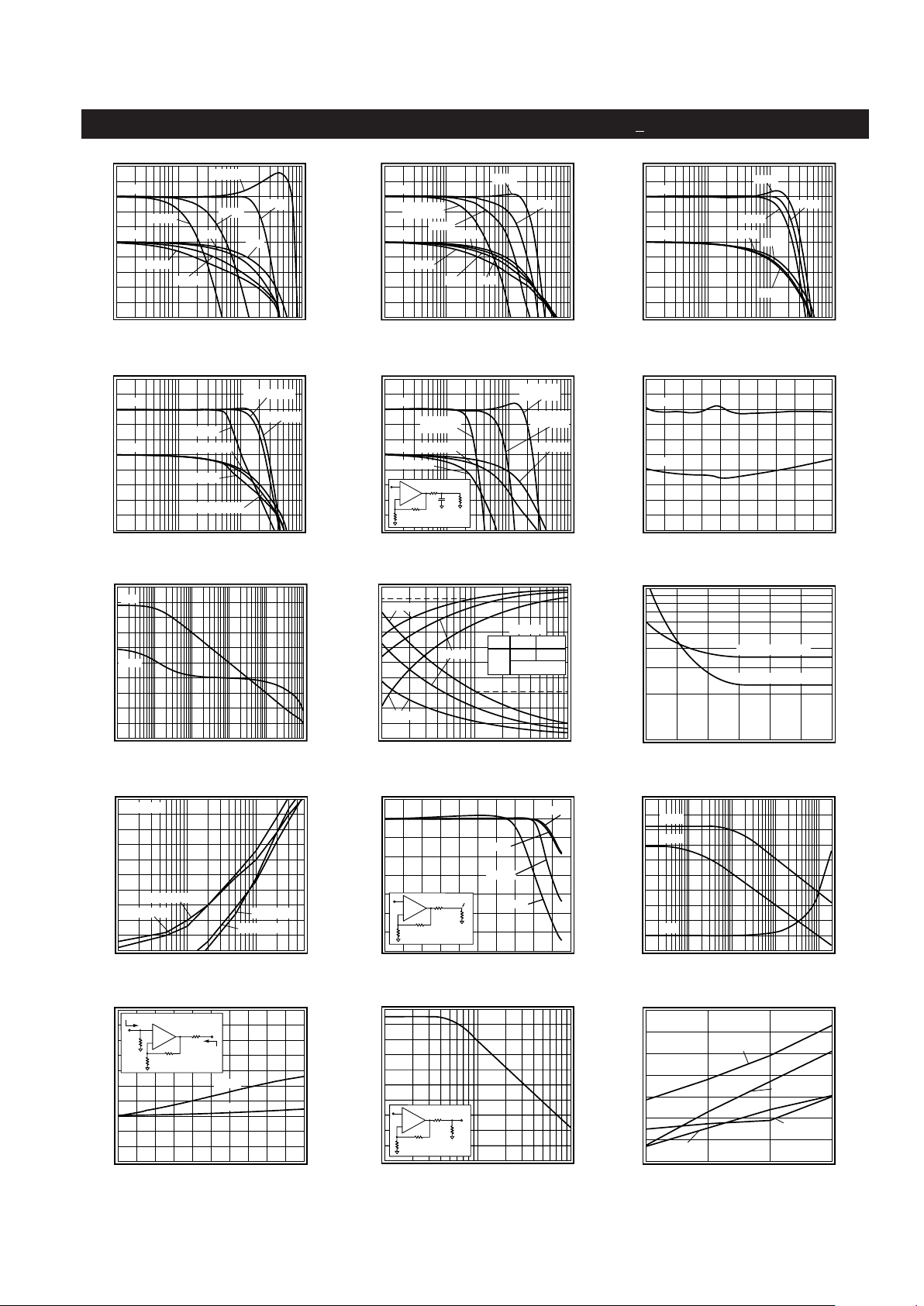
CLC440 Typical Performance Characteristics
(A
V
= +2, R
f
= 250Ω:V
cc
= + 5V, R
L
= 100Ω unless specified)
Non-Inverting Frequency Response
Magnitude (1dB/div)
Phase (deg)
-180
-90
-135
-45
0
1
10
100
Frequency (MHz)
A
V
= 10
A
V
= 2
A
V
= 1
A
V
= 1(R
f
= 0)
A
V
= 2
A
V
= 10
A
V
= 5
A
V
= 5
1000
Gain
Phase
Inverting Frequency Response
Magnitude (1dB/div)
Phase (deg)
-360
-270
-315
-225
-180
1
10
100
Frequency (MHz)
A
V
-10
A
V
-1
A
V
-2
A
V
= -1
A
V
= -2
A
V
= -10
(Rf = 500Ω)
A
V
= -5
A
V
-5
1000
Gain
Phase
Frequency Response vs. Load
Magnitude (1dB/div)
Phase (deg)
-180
-90
-135
-45
0
1
10
100
Frequency (MHz)
R
L
=1K
R
L
=100
R
L
=1K
R
L
=100
R
L
=50
R
L
=50
1000
Gain
Phase
Frequency Response vs. V
out
Magnitude (1dB/div)
Phase (deg)
-180
-90
-135
-45
0
1
10
100
Frequency (MHz)
V
out
= 200mV
pp
1000
Gain
Phase
V
out
= 2V
pp
V
out
= 5V
pp
V
out
= 5V
pp
V
out
= 200mV
pp
V
out
= 2V
pp
Frequency Response vs. Capacitive Load
Magnitude (1dB/div)
Phase (deg)
-180
-90
-135
-45
0
1
10
100
Frequency (MHz)
C
L
= 10pF
R
s
= 50
1000
Gain
Phase
C
L
= 100pF
R
s
= 30
C
L
= 1000pF
R
s
= 5
C
L
= 1000pF
C
L
= 100pF
C
L
= 10pF
+
-
R
s
1k
C
L
Gain Flatness and Linear Phase
Magnitude (0.05dB/div)
Phase (1.0deg/div)
0
Frequency (7.5MHz/div)
75
Gain
Phase
Open Loop Gain and Phase
Open Loop Gain (dB)
Phase (deg)
1k
Frequency (Hz)
100M
Gain
Phase
10k
100k 1M
10M
80
60
40
20
0
-20
0
-90
-180
-270
BW vs. Gain for Transimpedance Configuration
C
f
(pF)
100
1000
10000
R
f
0
4
8
16
20
Bandwidth (MHz)
400
320
240
80
0
12
160
C
d
= 1pF
C
d
= 5pF
C
d
= 20pF
BW
C
f
R
f
1000
C
f
1.6
BW
123
See dashed lines
Example
Equivalent Input Noise
Noise Voltage (nV/√Hz)
Frequency (Hz)
10
1
1k
100
10k
100k
1M
10M
Noise Current (pA/√Hz)
10
1
Voltage = 3.5nV/√Hz
Current = 2.5pA/√Hz
100M
Harmonic Distortion vs. Frequency
Distortion (dBc)
Frequency (MHz)
-45
-55
-95
0.1
1
10
-75
-85
-65
3rd R
L
= 100
2nd R
L
= 1k
3rd R
L
= 1k
2nd R
L
= 100
50
V
o
= 2V
pp
1dB Compression
Gain (1dB/div)
Output Power (P
out
)
-4
0
16
50MHz
100MHz
5MHz
20MHz
4812
+
-
50Ω
50Ω
Pout
250Ω
250Ω
Input and Output VSWR
VSWR
Frequency (20MHz/div)
0
200
Input
Output
1.0
1.4
1.8
2.2
40 80 120 160
+
-
50Ω
Output
50Ω
250Ω
50Ω
Input
PSRR, CMRR, and Closed Loop R
out
PSRR/CMRR (dB)
Frequency (Hz)
45
35
10k
100k
100M
15
25
100
80
40
0
60
5
1M 10M
20
CMRR
R
out
PSRR
R
out
(Ω)
Differential Gain and Phase
Differential Gain (%), Phase (deg)
Number of 150Ω Loads
0.12
1
2
3
0.04
0
0.08
Gain
Positive Sync
Phase
Negative Sync
4
Gain
Negative Sync
Phase
Positive Sync
2-Tone, 3rd Order Intermodulation Intercept
Intercept Point (+dBm)
1
10
100
Frequency (MHz)
50
40
30
20
10
0
+
-
50Ω
P
out
250Ω
250Ω
50Ω
3 http://www.national.com
 Loading...