


MOTOROLA MC14490P, MC14490DW, MC14490DWR2, MC14490FEL, MC14490FL1 Datasheet
...
MC14490
Hex Contact Bounce
Eliminator
The MC14490 is constructed with complementary MOS enhancement mode devices, and is used for the elimination of extraneous level changes that result when interfacing with mechanical contacts. The digital contact bounce eliminator circuit takes an input signal from a bouncing contact and generates a clean digital signal four clock periods after the input has stabilized. The bounce eliminator circuit will remove bounce on both the ªmakeº and the ªbreakº of a contact closure. The clock for operation of the MC14490 is derived from an internal R±C oscillator which requires only an external capacitor to adjust for the desired operating frequency (bounce delay). The clock may also be driven from an external clock source or the oscillator of another MC14490 (see Figure 5).
NOTE: Immediately after power±up, the outputs of the MC14490 are in indeterminate states.
•Diode Protection on All Inputs
•Six Debouncers Per Package
•Internal Pullups on All Data Inputs
•Can Be Used as a Digital Integrator, System Synchronizer, or Delay Line
•Internal Oscillator (R±C), or External Clock Source
•TTL Compatible Data Inputs/Outputs
•Single Line Input, Debounces Both ªMakeº and ªBreakº Contacts
•Does Not Require ªForm Cº (Single Pole Double Throw) Input Signal
•Cascadable for Longer Time Delays
•Schmitt Trigger on Clock Input (Pin 7)
•Supply Voltage Range = 3.0 V to 18 V
•Chip Complexity: 546 FETs or 136.5 Equivalent Gates
MAXIMUM RATINGS (Voltages Referenced to VSS) (Note 2.)
Symbol |
Parameter |
Value |
Unit |
|
|
|
|
VDD |
DC Supply Voltage Range |
± 0.5 to +18.0 |
V |
Vin, Vout |
Input or Output Voltage Range |
± 0.5 to VDD + 0.5 |
V |
|
(DC or Transient) |
|
|
|
|
|
|
Iin |
Input Current |
± 10 |
mA |
|
(DC or Transient) per Pin |
|
|
|
|
|
|
PD |
Power Dissipation, |
500 |
mW |
|
per Package (Note 3.) |
|
|
|
|
|
|
TA |
Ambient Temperature Range |
± 55 to +125 |
°C |
Tstg |
Storage Temperature Range |
± 65 to +150 |
°C |
TL |
Lead Temperature |
260 |
°C |
|
(8±Second Soldering) |
|
|
|
|
|
|
2.Maximum Ratings are those values beyond which damage to the device may occur.
3.Temperature Derating:
Plastic ªP and D/DWº Packages: ± 7.0 mW/C From 65_C To 125_C
http://onsemi.com
|
|
MARKING |
|
|
DIAGRAMS |
|
|
16 |
|
PDIP±16 |
MC14490P |
|
P SUFFIX |
|
|
AWLYYWW |
|
|
CASE 648 |
|
|
|
|
|
|
1 |
|
|
16 |
|
SOIC±16 |
14490 |
|
|
|
|
DW SUFFIX |
|
|
CASE 751G |
AWLYYWW |
|
|
|
|
|
1 |
|
|
16 |
|
SOEIAJ±16 |
MC14490 |
|
F SUFFIX |
|
|
AWLYWW |
|
|
CASE 966 |
|
|
|
|
|
|
1 |
A |
= Assembly Location |
|
WL or L = Wafer Lot |
|
|
YY or Y |
= Year |
|
WW or W = Work Week |
||
ORDERING INFORMATION |
||
Device |
Package |
Shipping |
MC14490DW |
SOIC±16 |
47/Rail |
MC14490DWR2 |
SOIC±16 |
1000/Tape & Reel |
MC14490F |
SOEIAJ±16 |
See Note 1. |
MC14490FEL |
SOEIAJ±16 |
See Note 1. |
MC14490P |
PDIP±16 |
25/Rail |
1.For ordering information on the EIAJ version of the SOIC packages, please contact your local ON Semiconductor representative.
This device contains protection circuitry to guard against damage due to high static voltages or electric fields. However, precautions must be taken to avoid applications of any voltage higher than maximum rated voltages to this high±impedance circuit. For proper operation, Vin and Vout should be constrained to the
range VSS v (Vin or Vout) v VDD.
Unused inputs must always be tied to an appropriate logic voltage level (e.g., either VSS or VDD). Unused outputs must be left open.
Semiconductor Components Industries, LLC, 2000 |
1 |
Publication Order Number: |
May, 2000 ± Rev. 4 |
|
MC14490/D |

MC14490
Ain 1
OSCin 7
OSCout 9
Bin 14
Cin 3
Din 12
Ein 5
Fin 10
PIN ASSIGNMENT
Ain |
|
1 |
16 |
VDD |
|
||||
|
||||
Bout |
|
2 |
15 |
Aout |
|
||||
|
||||
Cin |
|
3 |
14 |
Bin |
|
||||
Dout |
|
4 |
13 |
Cout |
|
||||
Ein |
|
5 |
12 |
Din |
|
||||
Fout |
|
6 |
11 |
Eout |
|
||||
OSCin |
|
7 |
10 |
Fin |
|
||||
VSS |
|
8 |
9 |
OSCout |
|
|
BLOCK DIAGRAM |
|
|
|
|
|
|
+VDD |
|
|
|
|
|
|
|
|
|
DATA |
|
|
1/2±BIT |
15 Aout |
|
|
4±BIT STATIC SHIFT REGISTER |
||||||
|
DELAY |
|
|||||
|
SHIFT |
LOAD |
|
|
|
||
|
|
|
|
|
|
||
OSCILLATOR |
φ 1 |
|
|
|
φ 1 |
φ 2 |
VDD = PIN 16 |
AND |
|
φ 1 |
φ 2 |
VSS = PIN 8 |
|||
|
|
|
|||||
TWO±PHASE |
|
|
|
|
|
|
|
CLOCK GENERATOR |
φ 2 |
φ 1 |
|
φ 2 |
|
|
|
|
|
|
|
|
|
||
|
IDENTICAL TO ABOVE STAGE |
|
|
|
2 |
Bout |
|
|
|
φ 1 |
|
φ 2 |
|
|
|
|
IDENTICAL TO ABOVE STAGE |
|
|
13 |
Cout |
|
|
||||
|
φ 1 |
φ 2 |
|
|
|
|
|
|
|
|
|
|
IDENTICAL TO ABOVE STAGE |
|
|
4 |
Dout |
|
|
||||
|
φ 1 |
φ 2 |
|
|
|
|
|
|
|
|
|
|
IDENTICAL TO ABOVE STAGE |
|
|
11 Eout |
|
|
|
|
|||
|
φ 1 |
φ 2 |
|
|
|
|
|
|
|
6 |
Fout |
|
IDENTICAL TO ABOVE STAGE |
|
|
||
|
|
||||
http://onsemi.com
2

MC14490
ELECTRICAL CHARACTERISTICS (Voltages Referenced to VSS)
|
|
|
VDD |
± 55_C |
|
25_C |
|
125_C |
|
||
|
|
|
|
|
|
|
|
|
|
|
|
Characteristic |
|
Symbol |
Vdc |
Min |
Max |
Min |
Typ (4.) |
Max |
Min |
Max |
Unit |
Output Voltage |
ª0º Level |
VOL |
5.0 |
Ð |
0.05 |
Ð |
0 |
0.05 |
Ð |
0.05 |
Vdc |
Vin = VDD or 0 |
|
|
10 |
Ð |
0.05 |
Ð |
0 |
0.05 |
Ð |
0.05 |
|
|
|
|
15 |
Ð |
0.05 |
Ð |
0 |
0.05 |
Ð |
0.05 |
|
|
|
|
|
|
|
|
|
|
|
|
|
|
ª1º Level |
VOH |
5.0 |
4.95 |
Ð |
4.95 |
5.0 |
Ð |
4.95 |
Ð |
Vdc |
Vin = 0 or VDD |
|
|
10 |
9.95 |
Ð |
9.95 |
10 |
Ð |
9.95 |
Ð |
|
|
|
|
15 |
14.95 |
Ð |
14.95 |
15 |
Ð |
14.95 |
Ð |
|
|
|
|
|
|
|
|
|
|
|
|
|
Input Voltage |
ª0º Level |
VIL |
|
|
|
|
|
|
|
|
Vdc |
(VO = 4.5 or 0.5 Vdc) |
|
|
5.0 |
Ð |
1.5 |
Ð |
2.25 |
1.5 |
Ð |
1.5 |
|
(VO = 9.0 or 1.0 Vdc) |
|
|
10 |
Ð |
3.0 |
Ð |
4.50 |
3.0 |
Ð |
3.0 |
|
(VO = 13.5 or 1.5 Vdc) |
|
|
15 |
Ð |
4.0 |
Ð |
6.75 |
4.0 |
Ð |
4.0 |
|
(VO = 0.5 or 4.5 Vdc) |
ª1 Levelº |
|
|
|
|
|
|
|
|
|
|
VIH |
5.0 |
3.5 |
Ð |
3.5 |
2.75 |
Ð |
3.5 |
Ð |
Vdc |
||
(VO = 1.0 or 9.0 Vdc) |
|
|
10 |
7.0 |
Ð |
7.0 |
5.50 |
Ð |
7.0 |
Ð |
|
(VO = 1.5 or 13.5 Vdc) |
|
|
15 |
11 |
Ð |
11 |
8.25 |
Ð |
11 |
Ð |
|
Output Drive Current |
|
IOH |
|
|
|
|
|
|
|
|
mAdc |
Oscillator Output |
Source |
|
|
|
|
|
|
|
|
|
|
(VOH = 2.5 V) |
|
|
5.0 |
± 0.6 |
Ð |
± 0.5 |
± 1.5 |
Ð |
± 0.4 |
Ð |
|
(VOH = 4.6 V) |
|
|
5.0 |
± 0.12 |
Ð |
± 0.1 |
± 0.3 |
Ð |
± 0.08 |
Ð |
|
(VOH = 9.5 V) |
|
|
10 |
± 0.23 |
Ð |
± 0.2 |
± 0.8 |
Ð |
± 0.16 |
Ð |
|
(VOH = 13.5 V) |
|
|
15 |
± 1.4 |
Ð |
± 1.2 |
± 3.0 |
Ð |
± 1.0 |
Ð |
|
Debounce Outputs |
|
|
|
|
|
|
|
|
|
|
|
(VOH = 2.5 V) |
|
|
5.0 |
± 0.9 |
Ð |
± 0.75 |
± 2.2 |
Ð |
± 0.6 |
Ð |
|
(VOH = 4.6 V) |
|
|
5.0 |
± 0.19 |
Ð |
± 0.16 |
± 0.46 |
Ð |
± 0.12 |
Ð |
|
(VOH = 9.5 V) |
|
|
10 |
± 0.6 |
Ð |
± 0.5 |
± 1.2 |
Ð |
± 0.4 |
Ð |
|
(VOH = 13.5 V) |
|
|
15 |
1.8 |
Ð |
± 1.5 |
± 4.5 |
Ð |
± 1.2 |
Ð |
|
Oscillator Output |
Sink |
IOL |
5.0 |
0.36 |
Ð |
0.3 |
0.9 |
Ð |
0.24 |
Ð |
mAdc |
(VOL = 0.4 V) |
|
|
|
||||||||
(VOL = 0.5 V) |
|
|
10 |
0.9 |
Ð |
0.75 |
2.3 |
Ð |
0.6 |
Ð |
|
(VOL = 1.5 V) |
|
|
15 |
4.2 |
Ð |
3.5 |
10 |
Ð |
2.8 |
Ð |
|
Debounce Outputs |
|
|
5.0 |
2.6 |
Ð |
2.2 |
4.0 |
Ð |
1.8 |
Ð |
|
(VOL = 0.4 V) |
|
|
|
||||||||
(VOL = 0.5 V) |
|
|
10 |
4.0 |
Ð |
3.3 |
9.0 |
Ð |
2.7 |
Ð |
|
(VOL = 1.5 V) |
|
|
15 |
12 |
Ð |
10 |
35 |
Ð |
8.1 |
Ð |
|
Input Current |
|
IIH |
15 |
Ð |
2.0 |
Ð |
0.2 |
2.0 |
Ð |
11 |
μAdc |
Debounce Inputs (Vin = VDD) |
|
|
|
|
|
|
|
|
|
|
|
Input Current Oscillator Ð Pin 7 |
Iin |
15 |
Ð |
± 620 |
Ð |
± 255 |
± 400 |
Ð |
± 250 |
μAdc |
|
(Vin = VSS or VDD) |
|
|
|
|
|
|
|
|
|
|
|
Pullup Resistor Source Current |
IIL |
5.0 |
175 |
375 |
140 |
190 |
255 |
70 |
225 |
μAdc |
|
Debounce Inputs |
|
|
10 |
340 |
740 |
280 |
380 |
500 |
145 |
440 |
|
(Vin = VSS) |
|
|
15 |
505 |
1100 |
415 |
570 |
750 |
215 |
660 |
|
Input Capacitance |
|
Cin |
Ð |
Ð |
Ð |
Ð |
5.0 |
7.5 |
Ð |
Ð |
pF |
Quiescent Current |
|
ISS |
5.0 |
Ð |
150 |
Ð |
40 |
100 |
Ð |
90 |
μAdc |
(Vin = VSS or VDD, Iout = 0 μA) |
|
10 |
Ð |
280 |
Ð |
90 |
225 |
Ð |
180 |
|
|
|
|
|
15 |
Ð |
840 |
Ð |
225 |
650 |
Ð |
550 |
|
|
|
|
|
|
|
|
|
|
|
|
|
4. Data labelled ªTypº is not to be used for design purposes but is intended as an indication of the IC's potential performance.
http://onsemi.com
3
MC14490
SWITCHING CHARACTERISTICS (5.) (CL = 50 pF, TA = 25_C)
|
|
|
VDD |
|
|
Typ (6.) |
|
|
|
||
|
Characteristic |
Symbol |
Vdc |
Min |
|
|
Max |
Unit |
|||
|
|
|
|
|
|
|
|
|
|
|
|
Output Rise Time |
|
tTLH |
5.0 |
Ð |
|
|
180 |
|
360 |
ns |
|
All Outputs |
|
|
10 |
Ð |
|
|
90 |
|
180 |
|
|
|
|
|
15 |
Ð |
|
|
65 |
|
130 |
|
|
|
|
|
|
|
|
|
|
|
|
|
|
Output Fall Time |
Oscillator Output |
|
5.0 |
Ð |
|
|
100 |
|
200 |
ns |
|
|
|
tTHL |
10 |
Ð |
|
|
50 |
|
100 |
|
|
|
|
|
15 |
Ð |
|
|
40 |
|
80 |
|
|
|
|
|
|
|
|
|
|
|
|
|
|
|
Debounce Outputs |
tTHL |
5.0 |
Ð |
|
|
60 |
|
120 |
|
|
|
|
|
10 |
Ð |
|
|
30 |
|
60 |
|
|
|
|
|
15 |
Ð |
|
|
20 |
|
40 |
|
|
|
|
|
|
|
|
|
|
|
|
||
Propagation Delay Time |
tPHL |
5.0 |
Ð |
|
|
285 |
|
570 |
ns |
||
Oscillator Input to Debounce Outputs |
|
10 |
Ð |
|
|
120 |
|
240 |
|
||
|
|
|
15 |
Ð |
|
|
95 |
|
190 |
|
|
|
|
|
|
|
|
|
|
|
|
|
|
|
|
tPLH |
5.0 |
Ð |
|
|
370 |
|
740 |
|
|
|
|
|
10 |
Ð |
|
|
160 |
|
320 |
|
|
|
|
|
15 |
Ð |
|
|
120 |
|
240 |
|
|
|
|
|
|
|
|
|
|
|
|
||
Clock Frequency (50% Duly Cycle) |
fcl |
5.0 |
Ð |
|
|
2.8 |
|
1.4 |
MHz |
||
(External Clock) |
|
|
10 |
Ð |
|
|
6 |
|
3.0 |
|
|
|
|
|
15 |
Ð |
|
|
9 |
|
4.5 |
|
|
|
|
|
|
|
|
|
|
|
|
||
Setup Time (See Figure 1) |
tsu |
5.0 |
100 |
|
|
50 |
|
Ð |
ns |
||
|
|
|
10 |
80 |
|
|
40 |
|
Ð |
|
|
|
|
|
15 |
60 |
|
|
30 |
|
Ð |
|
|
|
|
|
|
|
|
|
|
|
|
|
|
Maximum External Clock Input |
tr, tf |
5.0 |
|
|
|
|
|
|
|
ns |
|
Rise and Fall Time |
|
10 |
|
|
No Limit |
|
|
||||
Oscillator Input |
|
|
15 |
|
|
|
|
|
|
|
|
|
|
|
|
|
|
|
|
|
|
|
|
Oscillator Frequency |
|
fosc, typ |
|
|
|
|
1.5 |
|
|
Hz |
|
OSCout |
|
|
5.0 |
|
|
C |
ext |
(in mF) |
|
|
|
Cext ≥ 100 pF* |
|
|
|
|
|
|
|
|
|
|
|
|
|
10 |
|
|
|
4.5 |
|
|
|
||
|
|
|
|
|
|
|
|
|
|||
Note: These equations are intended to be a design guide. |
|
|
|
Cext (in mF) |
|
|
|||||
|
|
|
|
|
|
||||||
Laboratory experimentation may be required. Formulas |
|
15 |
|
|
|
6.5 |
|
|
|
||
are typically ± 15% of actual frequencies. |
|
|
|
|
|
|
|
|
|
||
|
|
|
Cext (in mF) |
|
|
||||||
|
|
|
|
|
|
||||||
5.The formulas given are for the typical characteristics only at 25_C.
6.Data labelled ªTypº is not to be used for design purposes but is intended as an indication of the IC's potential performance.
*POWER±DOWN CONSIDERATIONS
Large values of Cext may cause problems when powering down the MC14490 because of the amount of energy stored in the capacitor. When a system containing this device is powered down, the capacitor may discharge through the input protection diodes at Pin 7 or the parasitic diodes at Pin 9. Current through these internal diodes must be limited to 10 mA, therefore the
turn±off time of the power supply must not be faster than t = (VDD ± VSS) Cext / (10 mA). For example, If VDD ± VSS = 15 V and Cext = 1 μF, the power supply must turn off no faster than t = (15 V) (1 μF) / 10 mA = 1.5 ms. This is usually not a problem because power supplies are heavily filtered and cannot discharge at this rate.
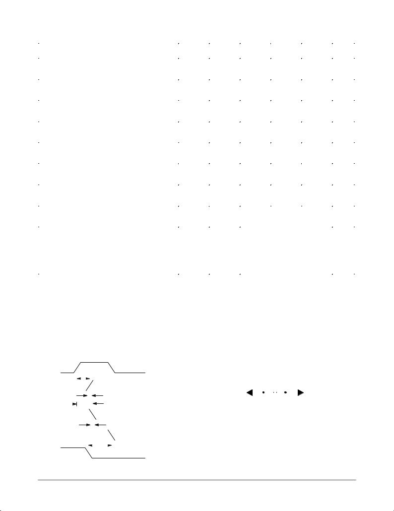
When a more rapid decrease of the power supply to zero volts occurs, the MC14490 may sustain damage. To avoid this possibility, use external clamping diodes, D1 and D2, connected as shown in Figure 2.
OSCin |
|
|
|
|
|
|
50% |
|
|
|
|
|
|
|
|
|
|
|
|
|
|
VDD |
|
|
|
|
|
|
|
|||||
|
|
|
|
|
|
|
|
|
|
|
|
|
|
|
|
|
|
|
|
|
|
|
|
|
|
|
||||||||
|
|
|
|
|
|
|
|
|
|
|
|
|
|
|
|
|
|
|
|
|
|
|
|
|
|
|
||||||||
|
|
|
|
|
|
|
|
|
|
|
|
|
|
|
|
|
|
|
|
0 V |
|
|
|
|
|
|
|
|||||||
|
|
|
|
|
|
|
|
|
|
|
|
|
|
|
|
|
|
|
|
|
|
|
|
|
|
|
|
|
|
|||||
|
tPLH |
|
|
|
|
|
|
|
|
|
|
|
|
|
|
|
|
|
|
|
|
|
|
|
|
|
|
|
|
|
|
|
||
Aout |
|
|
|
50% |
|
|
|
90% |
|
|
|
|
|
|
|
|
|
|
D1 |
Cext |
D2 |
|||||||||||||
|
|
|
|
|
10% |
|
|
|
|
|
|
|
|
|
|
|
||||||||||||||||||
|
|
|
|
|
|
|
|
|
|
tr |
VDD |
|
|
|
|
|
|
|
|
|
|
VDD |
||||||||||||
|
|
|
|
|
|
|
|
|
|
|
|
|
|
|
|
|
|
|
||||||||||||||||
|
|
|
|
|
|
|
|
|
|
|
|
|
|
|
|
|
|
|
|
|
|
|
|
|||||||||||
|
|
|
|
|
|
|
tPHL |
|
|
|
|
|
|
|
|
|
7 |
|
|
|
9 |
|
|
|
||||||||||
|
|
|
|
|
|
|
|
|
|
|
|
|
|
|
|
|
|
|
|
|
|
|
|
|
|
|||||||||
|
|
|
|
|
|
|
|
|
|
|
|
|
|
|
|
|
|
|
|
|
|
|
|
|||||||||||
Aout |
|
|
|
90% |
|
|
50% |
|
|
|
|
|
|
|
|
|
|
|
OSCin |
|
|
OSCout |
|
|
|
|||||||||
|
|
|
|
|
|
|
|
|
|
|
|
|
|
|
|
|||||||||||||||||||
|
|
|
10% |
|
|
|
|
|
|
|
|
|
|
|
|
|
|
|
|
|
|
|
|
|
|
|
|
|
|
|||||
OSCin |
|
|
|
|
|
|
|
|
|
|
|
|
|
tf |
VDD |
|
MC14490 |
|
|
|
||||||||||||||
|
|
|
|
|
|
|
|
|
|
|
|
|
|
|
|
|||||||||||||||||||
|
|
|
|
|
|
|
|
50% |
|
|
|
|
|
|
|
|
|
|
|
|
||||||||||||||
|
|
|
|
|
|
|
|
|
|
|
|
|
|
|
|
0 V |
|
|
|
|
||||||||||||||
|
|
|
|
|
|
|
|
|
|
|
|
|
|
|
|
|
|
|
||||||||||||||||
|
|
|
|
|
|
|
|
|
|
|
|
|
|
|
|
|
|
|
|
|
|
|
|
|
|
|
|
|
|
|
|
|||
|
|
|
|
|
|
|
|
|
|
|
|
|
|
|
|
|
|
|
|
|
|
|
|
|
|
|
|
|
|
|||||
Ain |
|
|
|
50% |
|
|
|
|
|
tsu |
|
|
|
VDD |
|
|
|
|
|
|
|
|
|
|||||||||||
|
|
|
|
|
|
|
|
|
|
|
|
|
|
|
|
|
|
|
|
|||||||||||||||
|
|
|
|
|
|
|
|
|
|
|
|
|
|
|
|
|
|
|
|
|
|
|
|
|
|
|
||||||||
|
|
|
|
|
|
|
|
|
|
|
|
|
|
|
|
|
|
|
|
|
|
|
|
|
||||||||||
|
|
|
|
|
|
|
|
|
|
|
|
|
|
|
|
|
|
|
|
|
|
|
0 V |
|
|
|
|
|
|
|
|
|
||
|
|
|
|
|
|
|
|
|
|
|
|
|
|
|
|
|
|
|
|
|
|
|
|
|
|
|
|
|
|
|||||
|
Figure 1. Switching Waveforms |
Figure 2. Discharge Protection During Power Down |
||||||||||||||||||||||||||||||||
http://onsemi.com
4
 Loading...