


MC14585B
4-Bit Magnitude
Comparator
The MC14585B 4±Bit Magnitude Comparator is constructed with complementary MOS (CMOS) enhancement mode devices. The circuit has eight comparing inputs (A3, B3, A2, B2, A1, B1, A0, B0), three cascading inputs (A < B, A = B, and A > B), and three outputs (A < B, A = B, and A > B). This device compares two 4±bit words (A and B) and determines whether they are ªless thanº, ªequal toº, or ªgreater thanº by a high level on the appropriate output. For words greater than 4±bits, units can be cascaded by connecting outputs (A > B), (A < B), and (A = B) to the corresponding inputs of the next significant comparator. Inputs (A < B), (A = B), and (A > B) on the least significant (first) comparator are connected to a low, a high, and a low, respectively.
Applications include logic in CPU's, correction and/or detection of instrumentation conditions, comparator in testers, converters, and controls.
•Diode Protection on All Inputs
•Expandable
•Applicable to Binary or 8421±BCD Code
•Supply Voltage Range = 3.0 Vdc to 18 Vdc
•Capable of Driving Two Low±power TTL Loads or One Low±power Schottky TTL Load over the Rated Temperature Range
•Can be Cascaded ± See Fig. 3
MAXIMUM RATINGS (Voltages Referenced to VSS) (Note 2.)
Symbol |
Parameter |
Value |
Unit |
|
|
|
|
VDD |
DC Supply Voltage Range |
± 0.5 to +18.0 |
V |
Vin, Vout |
Input or Output Voltage Range |
± 0.5 to VDD + 0.5 |
V |
|
(DC or Transient) |
|
|
|
|
|
|
Iin, Iout |
Input or Output Current |
±10 |
mA |
|
(DC or Transient) per Pin |
|
|
|
|
|
|
PD |
Power Dissipation, |
500 |
mW |
|
per Package (Note 3.) |
|
|
|
|
|
|
TA |
Ambient Temperature Range |
± 55 to +125 |
°C |
Tstg |
Storage Temperature Range |
± 65 to +150 |
°C |
TL |
Lead Temperature |
260 |
°C |
|
(8±Second Soldering) |
|
|
|
|
|
|
2.Maximum Ratings are those values beyond which damage to the device may occur.
3.Temperature Derating:
Plastic ªP and D/DWº Packages: ± 7.0 mW/C From 65_C To 125_C
This device contains protection circuitry to guard against damage due to high static voltages or electric fields. However, precautions must be taken to avoid applications of any voltage higher than maximum rated voltages to this high±impedance circuit. For proper operation, Vin and Vout should be constrained
to the range VSS v (Vin or Vout) v VDD.
Unused inputs must always be tied to an appropriate logic voltage level (e.g., either VSS or VDD). Unused outputs must be left open.
http://onsemi.com
|
|
MARKING |
|
|
DIAGRAMS |
|
|
16 |
|
PDIP±16 |
MC14585BCP |
|
P SUFFIX |
|
|
AWLYYWW |
|
|
CASE 648 |
|
|
|
|
|
|
1 |
|
|
16 |
|
SOIC±16 |
14585B |
|
D SUFFIX |
|
|
AWLYWW |
|
|
CASE 751B |
|
|
|
|
|
|
1 |
|
|
16 |
|
SOEIAJ±16 |
MC14585B |
|
F SUFFIX |
|
|
AWLYWW |
|
|
CASE 966 |
|
|
|
|
|
|
1 |
A |
= Assembly Location |
|
WL or L = Wafer Lot |
|
|
YY or Y |
= Year |
|
WW or W = Work Week |
||
ORDERING INFORMATION |
||
Device |
Package |
Shipping |
MC14585BCP |
PDIP±16 |
2000/Box |
MC14585BD |
SOIC±16 |
48/Rail |
MC14585BDR2 |
SOIC±16 |
2500/Tape & Reel |
MC14585BF |
SOEIAJ±16 |
See Note 1. |
1.For ordering information on the EIAJ version of the SOIC packages, please contact your local ON Semiconductor representative.
Semiconductor Components Industries, LLC, 2000 |
1 |
Publication Order Number: |
March, 2000 ± Rev. 3 |
|
MC14585B/D |
MC14585B
PIN ASSIGNMENT
B2 |
|
1 |
16 |
VDD |
|
||||
|
||||
A2 |
|
2 |
15 |
A3 |
(A = B)out |
|
3 |
14 |
B3 |
|
||||
|
||||
(A uB)in |
|
4 |
13 |
(A uB)out |
|
||||
|
||||
(A tB)in |
|
5 |
12 |
(A tB)out |
|
||||
|
||||
(A = B)in |
|
6 |
11 |
B0 |
|
||||
|
||||
A1 |
|
7 |
10 |
A0 |
|
||||
VSS |
|
8 |
9 |
B1 |
|
||||
|
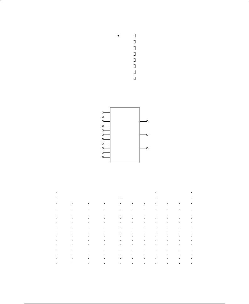
BLOCK DIAGRAM
4 |
(A > B)in |
|
|
6 |
(A = B)in |
|
|
5 |
(A < B)in |
(A > B)out |
13 |
10 |
A0 |
|
|
11 |
B0 |
|
|
7 |
A1 |
(A = B)out |
3 |
9 |
B1 |
|
|
2 |
A2 |
|
|
1 |
B2 |
(A < B)out |
12 |
15 |
A3 |
|
|
14 |
B3 |
|
|
VDD = PIN 16
VSS = PIN 8
TRUTH TABLE (x = Don't Care)
|
|
Inputs |
|
|
|
|
|
|
|
|
|
|
|
|
|
|
|
|
Outputs |
|
|
|
Comparing |
|
Cascading |
|
|
|||||
|
|
|
|
|
|
|
|
|
|
|
A3, B3 |
A2, B2 |
A1, B1 |
A0, B0 |
A < B |
A = B |
A > B |
A < B |
|
A = B |
A > B |
|
|
|
|
|
|
|
|
|
|
|
A3 > B3 |
x |
x |
x |
x |
x |
x |
0 |
|
0 |
1 |
A3 = B3 |
A2 > B2 |
x |
x |
x |
x |
x |
0 |
|
0 |
1 |
A3 = B3 |
A2 = B2 |
A1 > B1 |
x |
x |
x |
x |
0 |
|
0 |
1 |
A3 = B3 |
A2 = B2 |
A1 = B1 |
A0 > B0 |
x |
x |
x |
0 |
|
0 |
1 |
|
|
|
|
|
|
|
|
|
|
|
A3 = B3 |
A2 = B2 |
A1 = B1 |
A0 = B0 |
0 |
0 |
x |
0 |
|
0 |
1 |
A3 = B3 |
A2 = B2 |
A1 = B1 |
A0 = B0 |
0 |
1 |
x |
0 |
|
1 |
0 |
A3 = B3 |
A2 = B2 |
A1 = B1 |
A0 = B0 |
1 |
0 |
x |
1 |
|
0 |
0 |
A3 = B3 |
A2 = B2 |
A1 = B1 |
A0 = B0 |
1 |
1 |
x |
1 |
|
1 |
0 |
|
|
|
|
|
|
|
|
|
|
|
A3 = B3 |
A2 = B2 |
A1 = B1 |
A0 < B0 |
x |
x |
x |
1 |
|
0 |
0 |
A3 = B3 |
A2 = B2 |
A1 < B1 |
x |
x |
x |
x |
1 |
|
0 |
0 |
A3 = B3 |
A2 < B2 |
x |
x |
x |
x |
x |
1 |
|
0 |
0 |
|
|
|
|
|
|
|
|
|
|
|
A3 < B3 |
x |
x |
x |
x |
x |
x |
1 |
|
0 |
0 |
|
|
|
|
|
|
|
|
|
|
|
http://onsemi.com
2

MC14585B
ELECTRICAL CHARACTERISTICS (Voltages Referenced to VSS)
|
|
|
VDD |
± 55_C |
|
25_C |
|
|
125_C |
|
||
|
|
|
|
|
|
|
|
|
|
|
|
|
Characteristic |
|
Symbol |
Vdc |
Min |
Max |
Min |
Typ (4.) |
Max |
Min |
Max |
Unit |
|
Output Voltage |
ª0º Level |
VOL |
5.0 |
Ð |
0.05 |
Ð |
0 |
0.05 |
Ð |
0.05 |
Vdc |
|
Vin = VDD or 0 |
|
|
10 |
Ð |
0.05 |
Ð |
0 |
0.05 |
Ð |
0.05 |
|
|
|
|
|
15 |
Ð |
0.05 |
Ð |
0 |
0.05 |
Ð |
0.05 |
|
|
|
|
|
|
|
|
|
|
|
|
|
|
|
|
ª1º Level |
VOH |
5.0 |
4.95 |
Ð |
4.95 |
5.0 |
|
Ð |
4.95 |
Ð |
Vdc |
Vin = 0 or VDD |
|
|
10 |
9.95 |
Ð |
9.95 |
10 |
|
Ð |
9.95 |
Ð |
|
|
|
|
15 |
14.95 |
Ð |
14.95 |
15 |
|
Ð |
14.95 |
Ð |
|
|
|
|
|
|
|
|
|
|
|
|
|
|
Input Voltage |
ª0º Level |
VIL |
|
|
|
|
|
|
|
|
|
Vdc |
(VO = 4.5 or 0.5 Vdc) |
|
|
5.0 |
Ð |
1.5 |
Ð |
2.25 |
|
1.5 |
Ð |
1.5 |
|
(VO = 9.0 or 1.0 Vdc) |
|
|
10 |
Ð |
3.0 |
Ð |
4.50 |
|
3.0 |
Ð |
3.0 |
|
(VO = 13.5 or 1.5 Vdc) |
|
|
15 |
Ð |
4.0 |
Ð |
6.75 |
|
4.0 |
Ð |
4.0 |
|
(VO = 0.5 or 4.5 Vdc) |
ª1º Level |
VIH |
5.0 |
3.5 |
Ð |
3.5 |
2.75 |
|
Ð |
3.5 |
Ð |
Vdc |
|
|
|
|
|||||||||
(VO = 1.0 or 9.0 Vdc) |
|
|
10 |
7.0 |
Ð |
7.0 |
5.50 |
|
Ð |
7.0 |
Ð |
|
(VO = 1.5 or 13.5 Vdc) |
|
|
15 |
11 |
Ð |
11 |
8.25 |
|
Ð |
11 |
Ð |
|
Output Drive Current |
|
IOH |
|
|
|
|
|
|
|
|
|
mAdc |
(VOH = 2.5 Vdc) |
Source |
|
5.0 |
± 3.0 |
Ð |
± 2.4 |
± 4.2 |
|
Ð |
± 1.7 |
Ð |
|
(VOH = 4.6 Vdc) |
|
|
5.0 |
± 0.64 |
Ð |
± 0.51 |
± 0.88 |
|
Ð |
± 0.36 |
Ð |
|
(VOH = 9.5 Vdc) |
|
|
10 |
± 1.6 |
Ð |
± 1.3 |
± 2.25 |
|
Ð |
± 0.9 |
Ð |
|
(VOH = 13.5 Vdc) |
|
|
15 |
± 4.2 |
Ð |
± 3.4 |
± 8.8 |
|
Ð |
± 2.4 |
Ð |
|
(VOL = 0.4 Vdc) |
Sink |
IOL |
5.0 |
0.64 |
Ð |
0.51 |
0.88 |
|
Ð |
0.36 |
Ð |
mAdc |
(VOL = 0.5 Vdc) |
|
|
10 |
1.6 |
Ð |
1.3 |
2.25 |
|
Ð |
0.9 |
Ð |
|
(VOL = 1.5 Vdc) |
|
|
15 |
4.2 |
Ð |
3.4 |
8.8 |
|
Ð |
2.4 |
Ð |
|
Input Current |
|
Iin |
15 |
Ð |
± 0.1 |
Ð |
± 0.00001 |
± 0.1 |
Ð |
± 1.0 |
μAdc |
|
Input Capacitance |
|
Cin |
Ð |
Ð |
Ð |
Ð |
5.0 |
|
7.5 |
Ð |
Ð |
pF |
(Vin = 0) |
|
|
|
|
|
|
|
|
|
|
|
|
Quiescent Current |
|
IDD |
5.0 |
Ð |
5.0 |
Ð |
0.005 |
|
5.0 |
Ð |
150 |
μAdc |
(Per Package) |
|
|
10 |
Ð |
10 |
Ð |
0.010 |
|
10 |
Ð |
300 |
|
|
|
|
15 |
Ð |
20 |
Ð |
0.015 |
|
20 |
Ð |
600 |
|
|
|
|
|
|
|
|
|
|
|
|
|
|
Total Supply Current (5.) (6.) |
I |
5.0 |
|
|
I = (0.6 μA/kHz) f + I |
DD |
|
|
μAdc |
|||
|
|
T |
|
|
|
T |
|
|
|
|
|
|
(Dynamic plus Quiescent, |
|
10 |
|
|
IT = (1.2 μA/kHz) f + IDD |
|
|
|
||||
Per Package) |
|
|
15 |
|
|
IT = (1.8 μA/kHz) f + IDD |
|
|
|
|||
(CL = 50 pF on all outputs, all |
|
|
|
|
|
|
|
|
|
|
|
|
buffers switching) |
|
|
|
|
|
|
|
|
|
|
|
|
|
|
|
|
|
|
|
|
|
|
|
|
|
4.Data labelled ªTypº is not to be used for design purposes but is intended as an indication of the IC's potential performance.
5.The formulas given are for the typical characteristics only at 25_C.
6.To calculate total supply current at loads other than 50 pF:
IT(CL) = IT(50 pF) + (CL ± 50) Vfk
where: IT is in μA (per package), CL in pF, V = (VDD ± VSS) in volts, f in kHz is input frequency, and k = 0.001.
http://onsemi.com
3
 Loading...