


MOTOROLA
SEMICONDUCTOR TECHNICAL DATA
Quad Precision Timer/Driver
MC14415 quad timer/driver is constructed with complementary MOS enhancement mode devices. The output pulse width of each digital timer is a function of the input clock frequency. Once the proper input sequence is detected the output buffer is set (turned on), and after 100 clock pulses are counted, the output buffer is reset (turned off).
The MC14415 was designed specifically for application in high speed line printers to provide the critical timing of the hammer drivers, but may be used in many applications requiring precision pulse widths.
•Four Precision Digital Time Delays
•Schmitt Trigger Clock Conditioning
•NPN Bipolar Output Drivers
•Timing Disable Capability Using Inhibit Output
•Positive or Negative Edge Strobing on the Inputs
•Synchronous Polynomial Counters Used for Delay Counting
MAXIMUM RATINGS* (Voltages Referenced to VSS)
Rating |
Symbol |
Value |
|
Unit |
|
|
|
|
|
DC Supply Voltage MC14415FL, FP,DW |
VDD |
± 0.5 to + |
18.0 |
V |
MC14415VL, VP |
|
± 0.5 to + 6.0 |
|
|
|
|
|
|
|
Input or Output Voltage (DC or Transient) |
Vin, Vout |
± 0.5 to VDD + 0.5 |
V |
|
Input Current (DC or Transient), per Pin |
Iin |
± 10 |
|
mA |
Output Current (DC or Transient), per Pin |
Iout |
± 20 |
|
mA |
Power Dissipation, per Package² |
PD |
500 |
|
mW |
Storage Temperature |
Tstg |
± 65 to + |
150 |
_C |
Lead Temperature (8±Second Soldering) |
TL |
260 |
|
_C |
* Maximum Ratings are those values beyond which damage to the device may occur. ²Temperature Derating:
Plastic ªP and D/DWº Packages: ± 7.0 mW/C From 65_C To 125_C Ceramic ªLº Packages: ± 12 mW/C From 100_C To 125_C
BLOCK DIAGRAM
SET A |
3 |
|
SET B |
4 |
INPUT |
SET C |
5 |
LOGIC |
SET D |
6 |
|
STROBE 2 |
9 |
|
STROBE 1 |
7 |
COMMON |
INPUT DISABLE 10 |
LOGIC |
|
|
||
OUTPUT SET |
2 |
|
CLOCK |
1 |
|
OUTPUT INHIBIT 15 
|
|
|
|
|
|
14 |
OUTPUT A |
|
|
|
|
|
|
||
|
DIVIDE±BY± |
|
OUTPUT |
|
13 |
OUTPUT B |
|
|
100 |
|
|
||||
|
|
BUFFERS |
|
12 |
OUTPUT C |
||
|
COUNTERS |
|
|
||||
|
|
|
|
|
11 OUTPUT D |
||
|
|
|
|
|
|
||
|
|
|
|
|
|
||
|
|
|
|
|
|
|
|
|
|
|
|
|
|
|
|
|
CLOCK |
|
|
|
VDD = PIN 16 |
||
|
CONDITIONING |
|
|
|
|||
|
CIRCUIT |
|
|
|
VSS = PIN 8 |
||
|
|
|
|
|
|
|
|
|
|
|
|
|
|
|
|
MC14415
L SUFFIX
CERAMIC
CASE 620
P SUFFIX
PLASTIC |
|
CASE 648 |
|
DW SUFFIX |
|
|
SOIC |
CASE 751G |
|
ORDERING INFORMATION |
|
MC14415FP (3.0 V±18 V) |
Plastic |
MC14415VP (3.0 V±6.0 V) |
Plastic |
MC14415FL (3.0 V±18 V) |
Ceramic |
MC14415VL (3.0 V±6.0 V) |
Ceramic |
MC14415DW (3.0 V±18 V) |
SOIC |
TA = ± 55° to 125°C for all packages.
PIN ASSIGNMENT
CLOCK |
|
1 |
16 |
|
|
VDD |
||||||
|
|
|
||||||||||
|
|
|
||||||||||
|
|
SET |
|
|
2 |
15 |
|
|
INH |
|
||
|
|
|
|
|
|
|||||||
SET A |
|
3 |
14 |
|
|
OUT A |
||||||
|
|
|
||||||||||
SET B |
|
4 |
13 |
|
|
OUT B |
||||||
|
|
|
||||||||||
SET C |
|
5 |
12 |
|
|
OUT C |
||||||
|
|
|
||||||||||
SET D |
|
6 |
11 |
|
|
OUT D |
||||||
|
|
|
||||||||||
|
|
|
1 |
|
7 |
10 |
|
|
|
|
|
|
ST |
|
|
DIS |
|||||||||
|
|
|
|
|
|
|||||||
|
VSS |
|
8 |
9 |
|
|
ST2 |
|||||
|
|
|
|
|||||||||
|
|
|
|
|||||||||
REV 3 1/94
Motorola, Inc. 1995

ELECTRICAL CHARACTERISTICS (Voltages Referenced to VSS)
|
|
|
|
VDD |
± 55_C |
|
25_C |
|
125_C |
|
||
|
|
|
|
|
|
|
|
|
|
|
|
|
|
Characteristic |
|
Symbol |
Vdc |
Min |
Max |
Min |
Typ # |
Max |
Min |
Max |
Unit |
|
|
|
|
|
|
|
|
|
|
|
|
|
Output Voltage |
ª0º Leve |
VOL |
5.0 |
Ð |
0.01 |
Ð |
0 |
0.01 |
Ð |
0.05 |
Vdc |
|
(No Load) |
|
|
10 |
Ð |
0.01 |
Ð |
0 |
0.01 |
Ð |
0.05 |
|
|
|
|
|
|
15 |
Ð |
Ð |
Ð |
Ð |
Ð |
Ð |
Ð |
|
|
|
|
|
|
|
|
|
|
|
|
|
|
|
|
ª1º Leve |
VOH |
5.0 |
Ð |
Ð |
3.0 |
4.14 |
Ð |
Ð |
Ð |
Vdc |
|
|
|
|
10 |
Ð |
Ð |
8.0 |
9.09 |
Ð |
Ð |
Ð |
|
|
|
|
|
15 |
Ð |
Ð |
Ð |
14.12 |
Ð |
Ð |
Ð |
|
|
|
|
|
|
|
|
|
|
|
|
|
|
Noise Immunity |
|
VNL |
|
|
|
|
|
|
|
|
Vdc |
|
( |
Vout v 1.5 Vdc) |
|
|
5.0 |
1.5 |
Ð |
1.5 |
2.25 |
Ð |
1.4 |
Ð |
|
( |
Vout v 3.0 Vdc) |
|
|
10 |
3.0 |
Ð |
3.0 |
4.50 |
Ð |
2.9 |
Ð |
|
( |
Vout v 4.5 Vdc) |
|
|
15 |
Ð |
Ð |
Ð |
6.75 |
Ð |
Ð |
Ð |
|
( |
Vout v 1.5 Vdc) |
|
VNH |
5.0 |
1.4 |
Ð |
1.5 |
2.25 |
Ð |
1.5 |
Ð |
Vdc |
( |
Vout v 3.0 Vdc) |
|
|
10 |
2.9 |
Ð |
3.0 |
4.50 |
Ð |
3.0 |
Ð |
|
( |
Vout v 4.5 Vdc) |
|
|
15 |
Ð |
Ð |
Ð |
6.75 |
Ð |
Ð |
Ð |
|
Output Drive Voltage (NPN Driver) |
VOH |
|
|
|
|
|
|
|
|
Vdc |
||
(IOH = 0 mA) |
Source |
|
5.0 |
Ð |
Ð |
3.0 |
4.14 |
Ð |
Ð |
Ð |
|
|
(IOH = 5.0 mA) |
|
|
|
Ð |
Ð |
2.7 |
3.44 |
Ð |
Ð |
Ð |
|
|
(IOH = 10 mA) |
|
|
|
Ð |
Ð |
2.5 |
3.30 |
Ð |
Ð |
Ð |
|
|
(IOH = 15 mA) |
|
|
|
Ð |
Ð |
2.2 |
3.08 |
Ð |
Ð |
Ð |
|
|
(IOH = 0 mA) |
|
|
10 |
Ð |
Ð |
8.0 |
9.09 |
Ð |
Ð |
Ð |
Vdc |
|
(IOH = 5.0 mA) |
|
|
|
Ð |
Ð |
7.7 |
8.45 |
Ð |
Ð |
Ð |
|
|
(IOH = 10 mA) |
|
|
|
Ð |
Ð |
7.5 |
8.30 |
Ð |
Ð |
Ð |
|
|
(IOH = 15 mA) |
|
|
|
Ð |
Ð |
7.1 |
8.14 |
Ð |
Ð |
Ð |
|
|
(IOH = 0 mA) |
|
|
15 |
Ð |
Ð |
Ð |
14.12 |
Ð |
Ð |
Ð |
Vdc |
|
(IOH = 5.0 mA) |
|
|
|
Ð |
Ð |
Ð |
13.81 |
Ð |
Ð |
Ð |
|
|
(IOH = 10 mA) |
|
|
|
Ð |
Ð |
Ð |
13.70 |
Ð |
Ð |
Ð |
|
|
(IOH = 15 mA) |
|
|
|
Ð |
Ð |
Ð |
13.61 |
Ð |
Ð |
Ð |
|
|
Output Drive Current |
|
IOL |
|
|
|
|
|
|
|
|
mAdc |
|
(VOL = 0.4 Vdc) |
Sink |
|
5.0 |
0.23 |
Ð |
0.2 |
0.78 |
Ð |
0.16 |
Ð |
|
|
(VOL = 0.5 Vdc) |
|
|
10 |
0.60 |
Ð |
0.5 |
2.0 |
Ð |
0.40 |
Ð |
|
|
(VOL = 1.5 Vdc) |
|
|
15 |
Ð |
Ð |
Ð |
7.8 |
Ð |
Ð |
Ð |
|
|
Input Leakage Current |
|
Iin |
15 |
Ð |
± 0.3 |
Ð |
± 0.00001 |
± 0.3 |
Ð |
± 1.0 |
μAdc |
|
Input Capacitance |
|
Cin |
Ð |
Ð |
Ð |
Ð |
5.0 |
Ð |
Ð |
Ð |
pF |
|
(Vin = 0) |
|
|
|
|
|
|
|
|
|
|
|
|
Quiescent Dissipation |
|
PQ |
5.0 |
Ð |
0.25 |
Ð |
0.00005 |
0.25 |
Ð |
3.5 |
mW |
|
|
|
|
|
10 |
Ð |
1.0 |
Ð |
0.00022 |
1.0 |
Ð |
14 |
|
|
|
|
|
15 |
Ð |
Ð |
Ð |
0.00050 |
Ð |
Ð |
Ð |
|
|
|
|
|
|
|
|
|
|
|
|
|
|
Power Dissipation** |
|
PD |
5.0 |
|
|
PD (56 mW/MHz) f + PQ |
|
|
mW |
|||
(Dynamic plus Quiescent) |
|
10 |
|
|
PD (225 mW/MHz) f + PQ |
|
|
|
||||
(CL = 15 pF) |
|
|
15 |
|
|
PD (510 mW/MHz) f + PQ |
|
|
|
|||
#Data labelled ªTypº is not to be used for design purposes but is intended as an indication of the IC's potential performance. ** The formulas given are for the typical characteristics only.
This device contains protection circuitry to guard against damage due to high static voltages or electric fields. However, precautions must be taken to avoid applications of any voltage higher than maximum rated voltages to this high-impedance
circuit. For proper operation, Vin and Vout should be constrained to the range VSS ≤ (Vin or Vout) ≤ VDD.
Unused inputs must always be tied to an appropriate logic voltage level (e.g., either VSS or VDD). Unused outputs must be left open.
MOTOROLA CMOS LOGIC DATA |
MC14415 |
|
291 |
SWITCHING CHARACTERISTICS* (CL = 15 pF, TA = 25_C)
|
|
|
|
|
|
VDD |
|
|
|
|
Characteristic |
Symbol |
Vdc |
Min |
Typ # |
Max |
Unit |
||||
|
|
|
|
|
|
|
|
|
|
|
Output Rise Time |
tTLH |
|
|
|
|
ns |
||||
tTLH = (2.0 ns/pF) CL + 10 ns |
|
5.0 |
Ð |
40 |
85 |
|
||||
tTLH = (1.25 ns/pF) CL + 6 ns |
|
10 |
Ð |
25 |
60 |
|
||||
tTLH = (1.10 ns/pF) CL + 3 ns |
|
15 |
Ð |
20 |
Ð |
|
||||
Output Fall Time |
tTHL |
|
|
|
|
ns |
||||
tTHL = (1.5 ns/pF) CL + 47 ns |
|
5.0 |
Ð |
70 |
150 |
|
||||
tTHL = (0.75 ns/pF) CL + 24 ns |
|
10 |
Ð |
35 |
80 |
|
||||
tTHL = (0.55 ns/pF) CL + 17 ns |
|
15 |
Ð |
25 |
Ð |
|
||||
Turn±Off Delay Time |
tPLH |
|
|
|
|
ns |
||||
tPLH = (2.7 ns/pF) CL + 560 ns |
|
5.0 |
Ð |
600 |
1200 |
|
||||
tPLH = (1.2 ns/pF) CL + 282 ns |
|
10 |
Ð |
300 |
600 |
|
||||
tPLH = (0.91 ns/pF) CL + 286 ns |
|
15 |
Ð |
150 |
Ð |
|
||||
Turn±On Delay Time |
tPHL |
|
|
|
|
ns |
||||
tPHL = (2.4 ns/pF) CL + 564 ns |
|
5.0 |
Ð |
600 |
1200 |
|
||||
tPHL = (1.0 ns/pF) CL + 285 ns |
|
10 |
Ð |
300 |
600 |
|
||||
tPHL = (0.75 ns/pF) CL + 289 ns |
|
15 |
Ð |
150 |
Ð |
|
||||
Turn±On Delay Time |
|
|
to Output) |
tPHL |
|
|
|
|
ns |
|
(Inhibit |
|
|
|
|
||||||
|
|
|
|
|
|
5.0 |
Ð |
300 |
550 |
|
|
|
|
|
|
|
10 |
Ð |
225 |
425 |
|
|
|
|
|
|
|
15 |
Ð |
110 |
Ð |
|
|
|
|
|
|
|
|
|
|
|
|
Turn±Off Delay Time |
|
|
to Output) |
tPLH |
|
|
|
|
ns |
|
(Inhibit |
|
|
|
|
||||||
|
|
|
|
|
|
5.0 |
Ð |
300 |
550 |
|
|
|
|
|
|
|
10 |
Ð |
225 |
425 |
|
|
|
|
|
|
|
15 |
Ð |
110 |
Ð |
|
|
|
|
|
|
|
|
|
|
||
Input Pulse Coincidence (Figure 3) |
PCmin |
5.0 |
500 |
450 |
Ð |
ns |
||||
|
|
|
|
|
|
|
||||
|
|
|
|
|
|
10 |
450 |
350 |
Ð |
|
|
|
|
|
|
|
15 |
Ð |
Ð |
Ð |
|
|
|
|
|
|
|
|
||||
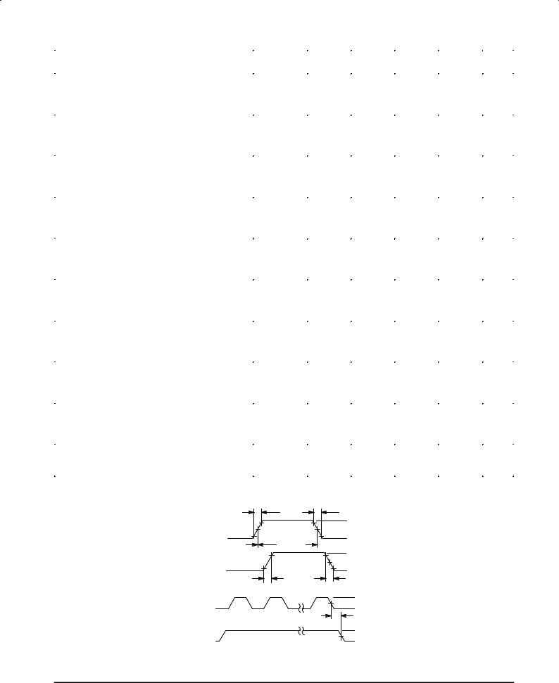
Input Pulse Width (Figure 1) |
tWH |
5.0 |
500 |
450 |
Ð |
ns |
||||
|
|
|
|
|
|
|
||||
|
|
|
|
|
|
10 |
450 |
350 |
Ð |
|
|
|
|
|
|
|
15 |
Ð |
Ð |
Ð |
|
|
|
|
|
|
|
|
||||
Input Clock Frequency |
fcl |
5.0 |
Ð |
0.7 |
Ð |
MHz |
||||
|
|
|
|
|
|
|
||||
|
|
|
|
|
|
10 |
Ð |
1.0 |
Ð |
|
|
|
|
|
|
|
15 |
Ð |
1.5 |
Ð |
|
|
|
|
|
|
|
|
||||
Clock Input Rise and Fall Times (Figure 1) |
tTLH, tTHL |
5.0 |
Ð |
Ð |
15 |
μs |
||||
|
|
|
|
|
|
10 |
Ð |
Ð |
5.0 |
|
|
|
|
|
|
|
15 |
Ð |
Ð |
4.0 |
|
|
|
|
|
|
|
|
|
|
|
|
* The formulas given are for the typical characteristics only at 25_C.
#Data labelled ªTypº is not to be used for design purposes but is intended as an indication of the IC's potential performance.
20 ns |
|
|
20 ns |
|||
INPUT |
|
50% |
90% |
|
VDD |
|
|
10% |
|
|
|||
|
|
|
|
VSS |
||
|
tPLH |
tWH |
|
|
||
|
|
|
VOH |
|||
OUTPUT |
|
90% |
|
50% |
||
10% |
|
|
|
|||
|
|
|
VOL |
|||
|
tTLH |
|
tTHL |
|
||
|
|
|
|
|||
CLOCK |
1 |
2 |
100 |
50% |
VDD |
|
VSS |
||||||
|
|
|
tPHL |
|
||
|
|
|
|
|
||
OUTPUT |
|
|
|
|
VOH |
|
|
|
|
|
VOL |
||
|
|
|
|
|
||
Figure 1. Switching Characteristics Ð Waveform Relationships |
||||||
MC14415 |
|
|
|
|
MOTOROLA CMOS LOGIC DATA |
|
292 |
|
|
|
|
|
|
 Loading...