


MOTOROLA MC14528BFL2, MC14528BFR1, MC14528BCP, MC14528BD, MC14528BDR2 Datasheet
...
MC14528B
Dual Monostable
Multivibrator
The MC14528B is a dual, retriggerable, resettable monostable multivibrator. It may be triggered from either edge of an input pulse, and produces an output pulse over a wide range of widths, the duration of which is determined by the external timing components, CX and RX.
•Separate Reset Available
•Diode Protection on All Inputs
•Triggerable from Leading or Trailing Edge Pulse
•Supply Voltage Range = 3.0 Vdc to 18 Vdc
•Capable of Driving Two Low±power TTL Loads or One Low±power Schottky TTL Load Over the Rated Temperature Range
•Pin±for±Pin Replacement with the MC14538B
MAXIMUM RATINGS (Voltages Referenced to VSS) (Note 2.)
Symbol |
Parameter |
Value |
Unit |
|
|
|
|
VDD |
DC Supply Voltage Range |
± 0.5 to +18.0 |
V |
Vin, Vout |
Input or Output Voltage Range |
± 0.5 to VDD + 0.5 |
V |
|
(DC or Transient) |
|
|
|
|
|
|
Iin, Iout |
Input or Output Current |
± 10 |
mA |
|
(DC or Transient) per Pin |
|
|
|
|
|
|
PD |
Power Dissipation, |
500 |
mW |
|
per Package (Note 3.) |
|
|
|
|
|
|
TA |
Ambient Temperature Range |
± 55 to +125 |
°C |
Tstg |
Storage Temperature Range |
± 65 to +150 |
°C |
TL |
Lead Temperature |
260 |
°C |
|
(8±Second Soldering) |
|
|
|
|
|
|
2.Maximum Ratings are those values beyond which damage to the device may occur.
3.Temperature Derating:
Plastic ªP and D/DWº Packages: ± 7.0 mW/C From 65_C To 125_C
This device contains protection circuitry to guard against damage due to high static voltages or electric fields. However, precautions must be taken to avoid applications of any voltage higher than maximum rated voltages to this high±impedance circuit. For proper operation, Vin and Vout should be constrained
to the range VSS v (Vin or Vout) v VDD.
Unused inputs must always be tied to an appropriate logic voltage level (e.g., either VSS or VDD). Unused outputs must be left open.
http://onsemi.com
|
|
MARKING |
|
|
DIAGRAMS |
|
|
16 |
|
PDIP±16 |
MC14528BCP |
|
P SUFFIX |
|
|
AWLYYWW |
|
|
CASE 648 |
|
|
|
|
|
|
1 |
|
|
16 |
|
SOIC±16 |
14528B |
|
D SUFFIX |
|
|
AWLYWW |
|
|
CASE 751B |
|
|
|
|
|
|
1 |
|
|
16 |
|
SOEIAJ±16 |
MC14528B |
|
F SUFFIX |
|
|
AWLYWW |
|
|
CASE 966 |
|
|
|
|
|
|
1 |
A |
= Assembly Location |
|
WL or L = Wafer Lot |
|
|
YY or Y |
= Year |
|
WW or W = Work Week |
||
ORDERING INFORMATION |
||
Device |
Package |
Shipping |
MC14528BCP |
PDIP±16 |
2000/Box |
MC14528BD |
SOIC±16 |
48/Rail |
MC14528BDR2 |
SOIC±16 |
2500/Tape & Reel |
MC14528BF |
SOEIAJ±16 |
See Note 1. |
MC14528BFEL |
SOEIAJ±16 |
See Note 1. |
1.For ordering information on the EIAJ version of the SOIC packages, please contact your local ON Semiconductor representative.
Semiconductor Components Industries, LLC, 2000 |
1 |
Publication Order Number: |
March, 2000 ± Rev. 3 |
|
MC14528B/D |
MC14528B
PIN ASSIGNMENT
VSS |
|
1 |
16 |
|
VDD |
|||
|
|
|||||||
|
|
|||||||
CX1/RX1 |
|
2 |
15 |
VSS |
||||
|
||||||||
RESET 1 |
|
|
3 |
14 |
|
CX2/RX2 |
||
|
|
|
||||||
|
A1 |
|
4 |
13 |
|
RESET 2 |
||
|
B1 |
|
5 |
12 |
|
A2 |
||
|
|
|
||||||
|
Q1 |
|
6 |
11 |
|
B2 |
||
|
|
|
||||||
|
|
|
|
7 |
10 |
|
Q2 |
|
|
Q1 |
|
|
|
||||
VSS |
|
8 |
9 |
|
|
|
||
|
|
Q2 |
|
|||||
|
|
|
||||||
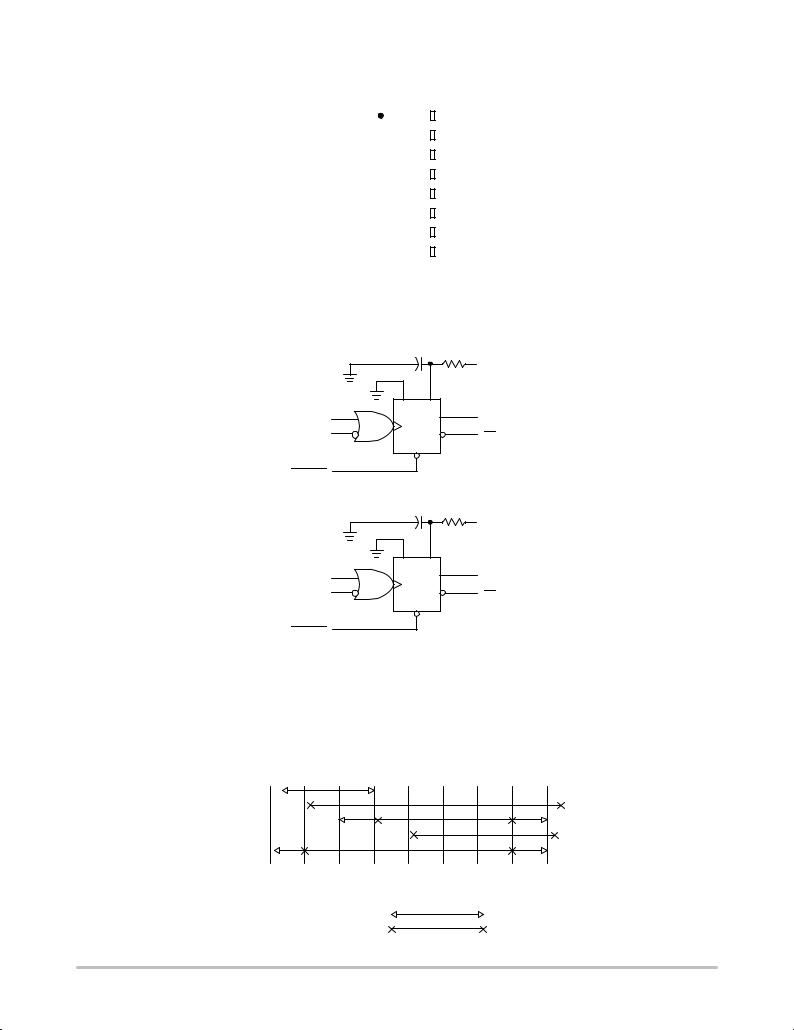
BLOCK DIAGRAM
|
CX1 |
RX1 |
VDD |
|
|
|
|
|
1 |
2 |
|
A1 |
4 |
6 |
Q1 |
|
|||
B1 |
5 |
7 |
Q1 |
3
RESET 1
|
CX2 |
R 2 |
|
|
|
|
X |
VDD |
|
|
|
|
||
|
15 |
14 |
|
|
A2 |
12 |
10 |
Q2 |
|
11 |
9 |
|||
|
||||
B2 |
Q2 |
RESET 2 13
VDD = PIN 16
VSS = PIN 1, PIN 8, PIN 15
RX AND CX ARE EXTERNAL COMPONENTS
|
ONE±SHOT SELECTION GUIDE |
|
|
|||
100 ns |
1 ms |
10 ms 100 ms |
1 ms |
10 ms 100 ms |
1 s |
10 s |
MC14528B |
|
|
|
|
|
|
MC14536B |
|
|
|
|
|
23 HR |
MC14538B |
|
|
|
|
|
|
MC14541B |
|
|
|
|
|
5 MIN. |
MC4538A* |
|
|
|
|
|
|
|
|
*LIMITED OPERATING VOLTAGE (2±6 V) |
|
|
||
TOTAL OUTPUT PULSE WIDTH RANGE
RECOMMENDED PULSE WIDTH RANGE
http://onsemi.com
2

MC14528B
ELECTRICAL CHARACTERISTICS (Voltages Referenced to VSS)
|
|
|
VDD |
± 55_C |
|
|
|
|
|
|
|
|
|
|
25_C |
|
|
|
|
|
125_C |
|
||
Characteristic |
|
Symbol |
Vdc |
Min |
Max |
|
Min |
|
|
|
|
Typ (4.) |
|
|
|
Max |
Min |
Max |
Unit |
|||||
Output Voltage |
ª0º Level |
VOL |
5.0 |
Ð |
0.05 |
|
|
Ð |
|
|
|
|
|
|
0 |
|
|
|
0.05 |
Ð |
0.05 |
Vdc |
||
Vin = VDD or 0 |
|
|
10 |
Ð |
0.05 |
|
|
Ð |
|
|
|
|
|
|
0 |
|
|
|
0.05 |
Ð |
0.05 |
|
||
|
|
|
15 |
Ð |
0.05 |
|
|
Ð |
|
|
|
|
|
|
0 |
|
|
|
0.05 |
Ð |
0.05 |
|
||
|
|
|
|
|
|
|
|
|
|
|
|
|
|
|
|
|
|
|
|
|
||||
|
ª1º Level |
VOH |
5.0 |
4.95 |
Ð |
|
4.95 |
|
|
|
|
|
5.0 |
|
|
|
Ð |
4.95 |
Ð |
Vdc |
||||
Vin = 0 or VDD |
|
|
10 |
9.95 |
Ð |
|
9.95 |
|
|
|
|
|
10 |
|
|
|
Ð |
9.95 |
Ð |
|
||||
|
|
|
15 |
14.95 |
Ð |
|
14.95 |
|
|
|
|
15 |
|
|
|
Ð |
14.95 |
Ð |
|
|||||
|
|
|
|
|
|
|
|
|
|
|
|
|
|
|
|
|
|
|
|
|
|
|
|
|
Input Voltage |
ª0º Level |
VIL |
|
|
|
|
|
|
|
|
|
|
|
|
|
|
|
|
|
|
|
|
|
Vdc |
(VO = 4.5 or 0.5 Vdc) |
|
|
5.0 |
Ð |
1.5 |
|
|
Ð |
|
|
|
|
|
|
2.25 |
|
|
|
1.5 |
Ð |
1.5 |
|
||
(VO = 9.0 or 1.0 Vdc) |
|
|
10 |
Ð |
3.0 |
|
|
Ð |
|
|
|
|
|
|
4.50 |
|
|
|
3.0 |
Ð |
3.0 |
|
||
(VO = 13.5 or 1.5 Vdc) |
|
|
15 |
Ð |
4.0 |
|
|
Ð |
|
|
|
|
|
|
6.75 |
|
|
|
4.0 |
Ð |
4.0 |
|
||
(VO = 0.5 or 4.5 Vdc) |
ª1º Level |
VIH |
5.0 |
3.5 |
Ð |
|
|
3.5 |
|
|
|
|
|
2.75 |
|
|
|
Ð |
3.5 |
Ð |
Vdc |
|||
|
|
|
|
|
|
|
|
|
|
|
|
|
||||||||||||
(VO = 1.0 or 9.0 Vdc) |
|
|
10 |
7.0 |
Ð |
|
|
7.0 |
|
|
|
|
|
5.50 |
|
|
|
Ð |
7.0 |
Ð |
|
|||
(VO = 1.5 or 13.5 Vdc) |
|
|
15 |
11 |
Ð |
|
|
11 |
|
|
|
|
|
|
8.25 |
|
|
|
Ð |
11 |
Ð |
|
||
Output Drive Current |
|
|
|
|
|
|
|
|
|
|
|
|
|
|
|
|
|
|
|
|
|
|
|
mAdc |
(VOH = 2.5 Vdc) |
Source |
|
5.0 |
± 1.2 |
Ð |
|
± 1.0 |
|
|
|
|
± 1.7 |
|
|
|
Ð |
± 0.7 |
Ð |
|
|||||
(VOH = 4.6 Vdc) |
|
IOH |
5.0 |
± 0.64 |
Ð |
|
± 0.51 |
|
|
|
|
± 0.88 |
|
|
|
Ð |
± 0.36 |
Ð |
|
|||||
(VOH = 9.5 Vdc) |
|
|
10 |
± 1.6 |
Ð |
|
± 1.3 |
|
|
|
|
± 2.25 |
|
|
|
Ð |
± 0.9 |
Ð |
|
|||||
(VOH = 13.5 Vdc) |
|
|
15 |
± 4.2 |
Ð |
|
± 3.4 |
|
|
|
|
± 8.8 |
|
|
|
Ð |
± 2.4 |
Ð |
|
|||||
(VOL = 0.4 Vdc) |
Sink |
|
5.0 |
0.64 |
Ð |
|
0.51 |
|
|
|
|
|
0.88 |
|
|
|
Ð |
0.36 |
Ð |
mAdc |
||||
(VOL = 0.5 Vdc) |
|
IOL |
10 |
1.6 |
Ð |
|
|
1.3 |
|
|
|
|
|
2.25 |
|
|
|
Ð |
0.9 |
Ð |
|
|||
(VOL = 1.5 Vdc) |
|
|
15 |
4.2 |
Ð |
|
|
3.4 |
|
|
|
|
|
8.8 |
|
|
|
Ð |
2.4 |
Ð |
|
|||
Input Current |
|
Iin |
15 |
Ð |
± 0.1 |
|
|
Ð |
|
|
|
|
± 0.00001 |
|
|
± 0.1 |
Ð |
± 1.0 |
μAdc |
|||||
Input Capacitance |
|
Cin |
Ð |
Ð |
Ð |
|
|
Ð |
|
|
|
|
|
|
5.0 |
|
|
|
7.5 |
Ð |
Ð |
pF |
||
(Vin = 0) |
|
|
|
|
|
|
|
|
|
|
|
|
|
|
|
|
|
|
|
|
|
|
|
|
Quiescent Current |
|
IDD |
5.0 |
Ð |
5.0 |
|
|
Ð |
|
|
|
|
|
|
0.005 |
|
|
|
5.0 |
Ð |
150 |
μAdc |
||
(Per Package) |
|
|
10 |
Ð |
10 |
|
|
Ð |
|
|
|
|
|
|
0.010 |
|
|
|
10 |
Ð |
300 |
|
||
|
|
|
15 |
Ð |
20 |
|
|
Ð |
|
|
|
|
|
|
0.015 |
|
|
|
20 |
Ð |
600 |
|
||
|
|
|
|
|
|
|
|
|
|
|
|
|
|
|
|
|
|
|
|
|
||||
Total Supply Current at an |
|
I |
Ð |
|
I (C |
L |
, C |
X |
) = [(C |
L |
+ 0.36C |
X |
)V |
DD |
f + 2x10±8 |
|
μAdc |
|||||||
|
|
T |
|
|
T |
|
|
|
|
|
|
|
|
|
|
|
|
|
|
|||||
external load Capacitance (C ) |
|
|
|
|
|
|
|
R |
X |
C |
X |
(V |
±2)2f] x 10±3 |
|
|
|
||||||||
|
L |
|
|
|
|
|
|
|
|
|
|
|
|
DD |
|
|
|
|
|
|
|
|
||
and at external timing |
|
|
|
where: IT in μA (per circuit), CL and CX in pF, RX in megohms, |
|
|||||||||||||||||||
capacitance (CX), use the |
|
|
|
VDD in Vdc, f in kHz is input frequency. |
|
|
||||||||||||||||||
formula Ð (5.) |
|
|
|
|
|
|
|
|
|
|
|
|
|
|
|
|
|
|
|
|
|
|
|
|
4.Data labelled ªTypº is not to be used for design purposes but is intended as an indication of the IC's potential performance.
5.The formulas given are for the typical characteristics only at 25_C.
http://onsemi.com
3

MC14528B
SWITCHING CHARACTERISTICS (8.) (CL = 50 pF, TA = 25_C)
|
|
|
|
|
|
|
|
|
|
|
|
|
|
|
|
|
|
CX |
RX |
VDD |
|
|
|
|
|
|
|
|
|
|
|
Characteristic |
Symbol |
pF |
kΩ |
Vdc |
Min |
|
Typ (9.) |
|
Max |
Unit |
|||||||||||
Output Rise and Fall Time |
|
|
|
|
|
|
|
|
|
|
tTLH, |
Ð |
Ð |
|
|
|
|
|
|
ns |
||||||
tTLH, tTHL = (1.5 ns/pF) CL + 25 ns |
tTHL |
|
|
5.0 |
Ð |
|
100 |
|
200 |
|
||||||||||||||||
tTLH, tTHL = (0.75 ns/pF) CL + 12.5 ns |
|
|
|
10 |
Ð |
|
50 |
|
100 |
|
||||||||||||||||
tTLH, tTHL = (0.55 ns/pF) CL + 9.5 ns |
|
|
|
15 |
Ð |
|
40 |
|
80 |
|
||||||||||||||||
|
|
|
|
|
|
|
|
|
|
|
|
|
|
|
|
|
tPLH, |
|
|
|
|
|
|
|
|
|
Turn±Off, Turn±On Delay Time Ð A or B to Q or Q |
|
15 |
5.0 |
|
|
|
|
|
|
ns |
||||||||||||||||
tPLH, tPHL = (1.7 ns/pF) CL + 240 ns |
tPHL |
|
|
5.0 |
Ð |
|
325 |
|
650 |
|
||||||||||||||||
tPLH, tPHL = (0.66 ns/pF) CL + 87 ns |
|
|
|
10 |
Ð |
|
120 |
|
240 |
|
||||||||||||||||
tPLH, tPHL = (0.5 ns/pF) CL + 65 ns |
|
|
|
15 |
Ð |
|
90 |
|
180 |
|
||||||||||||||||
|
|
|
|
|
|
|
|
|
tPLH, |
|
|
|
|
|
|
|
|
|
||||||||
Turn±Off, Turn±On Delay Time Ð A or B to Q or Q |
|
1000 |
10 |
|
|
|
|
|
|
ns |
||||||||||||||||
tPLH, tPHL = (1.7 ns/pF) CL + 620 ns |
tPHL |
|
|
5.0 |
Ð |
|
705 |
|
Ð |
|
||||||||||||||||
tPLH, tPHL = (0.66 ns/pF) CL + 257 ns |
|
|
|
10 |
Ð |
|
290 |
|
Ð |
|
||||||||||||||||
tPLH, tPHL = (0.5 ns/pF) CL + 185 ns |
|
|
|
15 |
Ð |
|
210 |
|
Ð |
|
||||||||||||||||
Input Pulse Width Ð A or B |
|
|
|
|
|
|
|
|
|
|
tWH |
15 |
5.0 |
5.0 |
150 |
|
70 |
|
Ð |
ns |
||||||
|
|
|
|
|
|
|
|
|
|
|
|
|
|
|
|
|
|
|
|
10 |
75 |
|
30 |
|
Ð |
|
|
|
|
|
|
|
|
|
|
|
|
|
|
|
|
|
|
|
|
|
15 |
55 |
|
30 |
|
Ð |
|
|
|
|
|
|
|
|
|
|
|
|
|
|
|
|
|
|
|
|
|
|
|
|
|
|
|
|
|
|
|
|
|
|
|
|
|
|
|
|
|
|
|
|
|
tWL |
1000 |
10 |
5.0 |
Ð |
|
70 |
|
Ð |
ns |
|
|
|
|
|
|
|
|
|
|
|
|
|
|
|
|
|
|
|
|
10 |
Ð |
|
30 |
|
Ð |
|
|
|
|
|
|
|
|
|
|
|
|
|
|
|
|
|
|
|
|
|
15 |
Ð |
|
30 |
|
Ð |
|
|
|
|
|
|
|
|
|
|
|
|
|
|
|
|
|
|
|
|
||||||||
|
|
|
|
|
|
|
|
|
|
|
|
|
|
|
|
|
tW |
|
|
|
|
|
|
|
|
|
Output Pulse Width Ð Q or Q |
|
|
|
|
|
|
|
15 |
5.0 |
5.0 |
Ð |
|
550 |
|
Ð |
ns |
||||||||||
(For CX < 0.01 μF use graph for |
|
|
|
10 |
Ð |
|
350 |
|
Ð |
|
||||||||||||||||
appropriate VDD level.) |
|
|
|
|
|
|
|
|
|
|
|
|
|
15 |
Ð |
|
300 |
|
Ð |
|
||||||
|
|
|
|
|
|
|
|
|
|
|
|
|
|
|
|
|
tW |
|
|
|
|
|
|
|
|
μs |
Output Pulse Width Ð Q or Q |
|
|
|
|
|
|
|
10,000 |
10 |
5.0 |
15 |
|
30 |
|
45 |
|||||||||||
(For CX > 0.01 μF use formula: |
|
|
|
10 |
10 |
|
50 |
|
90 |
|
||||||||||||||||
t |
= 0.2 R |
X |
C |
X |
Ln [V |
DD |
± V |
]) (6.) |
|
|
|
|
|
|
|
15 |
15 |
|
55 |
|
95 |
|
||||
W |
|
|
|
|
|
|
SS |
|
|
|
|
|
|
|
|
|
|
|
|
|
|
|
|
|||
Pulse Width Match between Circuits in the same |
t1 ± t2 |
10,000 |
10 |
5.0 |
Ð |
|
6.0 |
|
25 |
% |
||||||||||||||||
package |
|
|
|
|
|
|
|
|
|
|
|
|
|
|
|
|
|
|
10 |
Ð |
|
8.0 |
|
35 |
|
|
|
|
|
|
|
|
|
|
|
|
|
|
|
|
|
|
|
|
|
|
15 |
Ð |
|
8.0 |
|
35 |
|
|
|
|
|
|
|
|
|
|
|
|
|
|
|
|
|
|||||||||||
Reset Propagation Delay Ð |
|
|
|
to Q or |
|
|
tPLH, |
15 |
5.0 |
5.0 |
Ð |
|
325 |
|
600 |
ns |
||||||||||
Reset |
|
Q |
|
|
||||||||||||||||||||||
|
|
|
|
|
|
|
|
|
|
|
|
|
|
|
|
|
tPHL |
|
|
10 |
Ð |
|
90 |
|
225 |
|
|
|
|
|
|
|
|
|
|
|
|
|
|
|
|
|
|
|
|
|
15 |
Ð |
|
60 |
|
170 |
|
|
|
|
|
|
|
|
|
|
|
|
|
|
|
|
|
|
|
1000 |
10 |
5.0 |
Ð |
|
1000 |
|
Ð |
ns |
|
|
|
|
|
|
|
|
|
|
|
|
|
|
|
|
|
|
|
|
10 |
Ð |
|
300 |
|
Ð |
|
|
|
|
|
|
|
|
|
|
|
|
|
|
|
|
|
|
|
|
|
15 |
Ð |
|
250 |
|
Ð |
|
|
|
|
|
|
|
|
|
|
|
|
|
|
|
|
|
|
|
|
|
|
|
|
|
|
||
Retrigger Time |
|
|
|
|
|
|
|
|
|
|
|
|
|
|
trr |
15 |
5.0 |
5.0 |
0 |
|
Ð |
|
Ð |
ns |
||
|
|
|
|
|
|
|
|
|
|
|
|
|
|
|
|
|
|
|
|
10 |
0 |
|
Ð |
|
Ð |
|
|
|
|
|
|
|
|
|
|
|
|
|
|
|
|
|
|
|
|
|
15 |
0 |
|
Ð |
|
Ð |
|
|
|
|
|
|
|
|
|
|
|
|
|
|
|
|
|
|
|
1000 |
10 |
5.0 |
0 |
|
Ð |
|
Ð |
ns |
|
|
|
|
|
|
|
|
|
|
|
|
|
|
|
|
|
|
|
|
10 |
0 |
|
Ð |
|
Ð |
|
|
|
|
|
|
|
|
|
|
|
|
|
|
|
|
|
|
|
|
|
15 |
0 |
|
Ð |
|
Ð |
|
|
|
|
|
|
|
|
|
|
|
|
|
|
|
|
|
|
|
|
|
|
||||||
External Timing Resistance |
|
|
|
|
|
|
|
|
|
|
RX |
Ð |
Ð |
Ð |
5.0 |
|
Ð |
|
1000 |
kΩ |
||||||
External Timing Capacitance |
|
|
|
|
|
|
CX |
Ð |
Ð |
Ð |
|
No Limits (7.) |
|
μF |
||||||||||||
6.RX is in Ohms, CX is in farads, VDD and VSS in volts, PWout in seconds.
7.If CX > 15 μF, Use Discharge Protection Diode DX, per Fig. 9.
8.The formulas given are for the typical characteristics only at 25_C.
9.Data labelled ªTypº is not to be used for design purposes but is intended as an indication of the IC's potential performance.
http://onsemi.com
4
 Loading...