


MC14106B
Hex Schmitt Trigger
The MC14106B hex Schmitt Trigger is constructed with MOS P±channel and N±channel enhancement mode devices in a single monolithic structure. These devices find primary use where low power dissipation and/or high noise immunity is desired. The MC14106B may be used in place of the MC14069UB hex inverter for enhanced noise immunity or to ªsquare upº slowly changing waveforms.
•Increased Hysteresis Voltage Over the MC14584B
•Supply Voltage Range = 3.0 Vdc to 18 Vdc
•Capable of Driving Two Low±power TTL Loads or One Low±power Schottky TTL Load Over the Rated Temperature Range
•Pin±for±Pin Replacement for CD40106B and MM74C14
•Can Be Used to Replace the MC14584B or MC14069UB
MAXIMUM RATINGS (Voltages Referenced to VSS) (Note 1.)
Symbol |
Parameter |
Value |
Unit |
|
|
|
|
VDD |
DC Supply Voltage Range |
± 0.5 to +18.0 |
V |
Vin, Vout |
Input or Output Voltage Range |
± 0.5 to VDD + 0.5 |
V |
|
(DC or Transient) |
|
|
|
|
|
|
Iin, Iout |
Input or Output Current |
± 10 |
mA |
|
(DC or Transient) per Pin |
|
|
|
|
|
|
PD |
Power Dissipation, |
500 |
mW |
|
per Package (Note 2.) |
|
|
|
|
|
|
TA |
Ambient Temperature Range |
± 55 to +125 |
°C |
Tstg |
Storage Temperature Range |
± 65 to +150 |
°C |
TL |
Lead Temperature |
260 |
°C |
|
(8±Second Soldering) |
|
|
|
|
|
|
1.Maximum Ratings are those values beyond which damage to the device may occur.
2.Temperature Derating:
Plastic ªP and D/DWº Packages: ± 7.0 mW/C From 65_C To 125_C
This device contains protection circuitry to guard against damage due to high static voltages or electric fields. However, precautions must be taken to avoid applications of any voltage higher than maximum rated voltages to this high±impedance circuit. For proper operation, Vin and Vout should be constrained
to the range VSS v (Vin or Vout) v VDD.
Unused inputs must always be tied to an appropriate logic voltage level (e.g., either VSS or VDD). Unused outputs must be left open.
http://onsemi.com
|
|
MARKING |
|
|
DIAGRAMS |
|
|
14 |
|
PDIP±14 |
MC14106BCP |
|
P SUFFIX |
|
|
AWLYYWW |
|
|
CASE 646 |
|
|
|
|
|
|
1 |
|
|
14 |
|
SOIC±14 |
14106B |
|
D SUFFIX |
|
|
AWLYWW |
|
|
CASE 751A |
|
|
|
|
|
|
1 |
|
|
14 |
|
TSSOP±14 |
14 |
|
DT SUFFIX |
106B |
|
CASE 948G |
ALYW |
|
|
1 |
A |
= Assembly Location |
|
WL or L = Wafer Lot |
|
|
YY or Y |
= Year |
|
WW or W = Work Week |
|
|
ORDERING INFORMATION |
||
Device |
Package |
Shipping |
MC14106BCP |
PDIP±14 |
2000/Box |
MC14106BD |
SOIC±14 |
55/Rail |
MC14106BDR2 |
SOIC±14 |
2500/Tape & Reel |
MC14106BDT |
TSSOP±14 |
96/Rail |
MC14106BDTR2 |
TSSOP±14 |
2500/Tape & Reel |
Semiconductor Components Industries, LLC, 2000 |
1 |
Publication Order Number: |
March, 2000 ± Rev. 3 |
|
MC14106B/D |
MC14106B
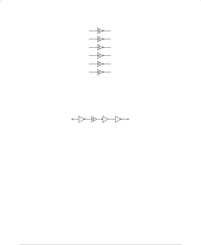
LOGIC DIAGRAM
1 |
2 |
3 |
4 |
5 |
6 |
9 |
8 |
11 |
10 |
13 |
12 |
|
VDD = PIN 14 |
|
VSS = PIN 7 |
EQUIVALENT CIRCUIT SCHEMATIC
(1/6 OF CIRCUIT SHOWN)
http://onsemi.com
2

MC14106B
ELECTRICAL CHARACTERISTICS (Voltages Referenced to VSS)
|
|
|
VDD |
± 55_C |
|
25_C |
|
|
125_C |
|
||
|
|
|
|
|
|
|
|
|
|
|
|
|
Characteristic |
|
Symbol |
Vdc |
Min |
Max |
Min |
Typ (3.) |
Max |
Min |
Max |
Unit |
|
Output Voltage |
ª0º Level |
VOL |
5.0 |
Ð |
0.05 |
Ð |
0 |
0.05 |
Ð |
0.05 |
Vdc |
|
Vin = VDD |
|
|
10 |
Ð |
0.05 |
Ð |
0 |
0.05 |
Ð |
0.05 |
|
|
|
|
|
15 |
Ð |
0.05 |
Ð |
0 |
0.05 |
Ð |
0.05 |
|
|
|
|
|
|
|
|
|
|
|
|
|
|
|
|
ª1º Level |
VOH |
5.0 |
4.95 |
Ð |
4.95 |
5.0 |
|
Ð |
4.95 |
Ð |
Vdc |
Vin = 0 |
|
|
10 |
9.95 |
Ð |
9.95 |
10 |
|
Ð |
9.95 |
Ð |
|
|
|
|
15 |
14.95 |
Ð |
14.95 |
15 |
|
Ð |
14.95 |
Ð |
|
|
|
|
|
|
|
|
|
|
|
|
|
|
Hysteresis Voltage |
|
V (6.) |
5.0 |
0.3 |
2.0 |
0.3 |
1.1 |
|
2.0 |
0.3 |
2.0 |
Vdc |
|
|
H |
10 |
1.2 |
3.4 |
1.2 |
1.7 |
|
3.4 |
1.2 |
3.4 |
|
|
|
|
|
|
||||||||
|
|
|
15 |
1.6 |
5.0 |
1.6 |
2.1 |
|
5.0 |
1.6 |
5.0 |
|
|
|
|
|
|
|
|
|
|
|
|
|
|
Threshold Voltage |
|
|
|
|
|
|
|
|
|
|
|
|
Positive±Going |
|
VT+ |
5.0 |
2.2 |
3.6 |
2.2 |
2.9 |
|
3.6 |
2.2 |
3.6 |
Vdc |
|
|
|
10 |
4.6 |
7.1 |
4.6 |
5.9 |
|
7.1 |
4.6 |
7.1 |
|
|
|
|
15 |
6.8 |
10.8 |
6.8 |
8.8 |
10.8 |
6.8 |
10.8 |
|
|
|
|
|
|
|
|
|
|
|
|
|
|
|
Negative±Going |
|
VT± |
5.0 |
0.9 |
2.8 |
0.9 |
1.9 |
|
2.8 |
0.9 |
2.8 |
Vdc |
|
|
|
10 |
2.5 |
5.2 |
2.5 |
3.9 |
|
5.2 |
2.5 |
5.2 |
|
|
|
|
15 |
4.0 |
7.4 |
4.0 |
5.8 |
|
7.4 |
4.0 |
7.4 |
|
|
|
|
|
|
|
|
|
|
|
|
|
|
Output Drive Current |
|
IOH |
|
|
|
|
|
|
|
|
|
mAdc |
(VOH = 2.5 Vdc) |
Source |
|
5.0 |
± 3.0 |
Ð |
± 2.4 |
± 4.2 |
|
Ð |
± 1.7 |
Ð |
|
(VOH = 4.6 Vdc) |
|
|
5.0 |
± 0.64 |
Ð |
± 0.51 |
± 0.88 |
|
Ð |
± 0.36 |
Ð |
|
(VOH = 9.5 Vdc) |
|
|
10 |
± 1.6 |
Ð |
± 1.3 |
± 2.25 |
|
Ð |
± 0.9 |
Ð |
|
(VOH = 13.5 Vdc) |
|
|
15 |
± 4.2 |
Ð |
± 3.4 |
± 8.8 |
|
Ð |
± 2.4 |
Ð |
|
(VOL = 0.4 Vdc) |
Sink |
IOL |
5.0 |
0.64 |
Ð |
0.51 |
0.88 |
|
Ð |
0.36 |
Ð |
mAdc |
(VOL = 0.5 Vdc) |
|
|
10 |
1.6 |
Ð |
1.3 |
2.25 |
|
Ð |
0.9 |
Ð |
|
(VOL = 1.5 Vdc) |
|
|
15 |
4.2 |
Ð |
3.4 |
8.8 |
|
Ð |
2.4 |
Ð |
|
Input Current |
|
Iin |
15 |
Ð |
± 0.1 |
Ð |
± 0.00001 |
± 0.1 |
Ð |
± 1.0 |
μAdc |
|
Input Capacitance |
|
Cin |
Ð |
Ð |
Ð |
Ð |
5.0 |
|
7.5 |
Ð |
Ð |
pF |
(Vin = 0) |
|
|
|
|
|
|
|
|
|
|
|
|
Quiescent Current |
|
IDD |
5.0 |
Ð |
0.25 |
Ð |
0.0005 |
0.25 |
Ð |
7.5 |
μAdc |
|
(Per Package) |
|
|
10 |
Ð |
0.5 |
Ð |
0.0010 |
|
0.5 |
Ð |
15 |
|
|
|
|
15 |
Ð |
1.0 |
Ð |
0.0015 |
|
1.0 |
Ð |
30 |
|
|
|
|
|
|
|
|
|
|
|
|
|
|
Total Supply Current (4.) (5.) |
I |
5.0 |
|
|
I = (1.8 μA/kHz) f + I |
DD |
|
|
μAdc |
|||
|
|
T |
|
|
|
T |
|
|
|
|
|
|
(Dynamic plus Quiescent, |
|
10 |
|
|
IT = (3.6 μA/kHz) f + IDD |
|
|
|
||||
Per Package) |
|
|
15 |
|
|
IT = (5.4 μA/kHz) f + IDD |
|
|
|
|||
(CL = 50 pF on all outputs, all |
|
|
|
|
|
|
|
|
|
|
|
|
buffers switching) |
|
|
|
|
|
|
|
|
|
|
|
|
|
|
|
|
|
|
|
|
|
|
|
|
|
3.Data labelled ªTypº is not to be used for design purposes but is intended as an indication of the IC's potential performance.
4.The formulas given are for the typical characteristics only at 25_C.
5.To calculate total supply current at loads other than 50 pF:
IT(CL) = IT(50 pF) + (CL ± 50) Vfk
where IT is in μA (per package), CL in pF, V = (VDD ± VSS) in volts, f in kHz is input frequency, and k = 0.001. 6. VH = VT+ ± VT± (But maximum variation of VH is specified as less that VT+ max ± VT± min).
http://onsemi.com
3
 Loading...