


MOTOROLA
SEMICONDUCTOR TECHNICAL DATA
128 Segment LCD Drivers
CMOS
The MC14LC5003/5004 are 128-segment, multiplexed-by-four LCD Drivers. The two devices are functionally the same except for their data input protocols. The MC14LC5003 uses a serial interface data input protocol. The device may be interfaced to the MC68HCXX product families using a minimal amount of software (see example). The MC14LC5004 has a IIC interface and has essentially the same protocol, except that the device sends an acknowledge bit back to the transmitter after each eight-bit byte is received. MC14LC5004 also has a “read mode”, whereby data sent to the device may be retrieved via the IIC bus.
The MC14LC5003/MC14LC5004 drives the liquid-crystal displays in a mul- tiplexed-by-four configuration. The device accepts data from a microprocessor or other serial data source to drive one segment per bit. The chip does not have a decoder, allowing for the flexibility of formatting the segment data externally.
Devices are independently addressable via a two-wire (or three-wire) communication link which can be common with other peripheral devices.
The MC14LC5003/MC14LC5004 are low cost version of MC145003 and MC145004 without cascading function.
•Drives 128 Segments Per Package
•May Be Used with the Following LCDs: Segmented Alphanumeric, Bar Graph, Dot Matrix, Custom
•Quiescent Supply Current: 30 Aµ @ 2.7 V VDD
•Operating Voltage Range: 2.7 to 5.5 V
•Operating Temperature Range: - 40 to 85C
•Separate Access to LCD Drive Section’s Supply Voltage to Allow for Temperature Compensation
•See Application Notes AN1066 and AN442
BLOCK DIAGRAM
BP1-BP4 |
FP1-FP32 |
VLCD |
|
OSC1 |
|
|
|
|
OSC2 |
|
OSCILLATOR |
DRIVERS |
|
|
|
|
DRIVERS |
|
|
|
FRAME |
|
|
|
|
SYNC |
LCD VOLTAGE |
128 - 32 |
|
|
GENERATOR |
||
|
|
|
WAVEFORM |
MULTIPLEX |
|
|
|
AND TIMING |
|
|
ADDRESSANDDATA |
POR |
GENERATOR |
|
DCLK |
TIMINGANDCONTROL |
128-BIT SHIFT REGISTER |
|
|
|
|
|
|
|
Din |
|
|
|
|
A0 |
|
|
128-BIT LATCH |
|
|
|
|
|
|
A1 |
|
|
|
|
A2 |
|
|
|
|
ENB |
|
|
|
|
MC14LC5003
MC14LC5004
|
QFP |
|
FU SUFFIX |
|
CASE 848B |
52 |
1 |
ORDERING INFORMATION
MC14LC5003FU |
QFP |
MC14LC5004FU |
QFP |
MCC14LC5003 |
BARE DIE |
MCC14LC5004 |
BARE DIE |
PIN ASSIGNMENT
|
|
NC |
OSC1 |
OSC2 |
V |
BP1 |
BP2 |
BP3 |
BP4 |
A0 A1 A2 |
ENB |
NC |
|
|
|
|
|
|
DD |
|
|
|
|
|
|
|
|
|
|
|
|
||||||||||
|
|
|
|
|
|
|
|
|
|
|
|
|
|
|
|
52 51 50 49 48 47 46 45 44 43 42 41 40 |
|
||||||||||
FP32 |
|
1 |
|
|
|
|
|
|
|
|
|
39 |
Din |
|
|
|
|
|
|
|
|
|
|
||||
FP31 |
|
2 |
|
|
|
|
|
|
|
|
|
38 |
DCLK |
|
|
|
|
|
|
|
|
|
|
||||
FP30 |
|
3 |
|
|
|
|
|
|
|
|
|
37 |
NC |
|
|
|
|
|
|
|
|
|
|
||||
FP29 |
|
4 |
|
|
|
|
|
|
|
|
|
36 |
FP1 |
|
|
|
|
|
|
|
|
|
|
||||
FP28 |
|
5 |
|
|
|
|
|
|
|
|
|
35 |
FP2 |
|
|
|
|
|
|
|
|
|
|
||||
FP27 |
|
6 |
|
|
|
|
|
|
|
|
|
34 |
FP3 |
|
|
|
|
|
|
|
|
|
|
||||
FP26 |
|
7 |
|
|
|
|
|
|
|
|
|
33 |
FP4 |
|
|
|
|
|
|
|
|
|
|
||||
FP25 |
|
8 |
|
|
|
|
|
|
|
|
|
32 |
FP5 |
|
|
|
|
|
|
|
|
|
|
||||
FP24 |
|
9 |
|
|
|
|
|
|
|
|
|
31 |
FP6 |
|
|
|
|
|
|
|
|
|
|
||||
FP23 |
|
10 |
|
|
|
|
|
|
|
|
|
30 |
FP7 |
|
|
|
|
|
|
|
|
|
|
||||
FP22 |
|
11 |
|
|
|
|
|
|
|
|
|
29 |
FP8 |
|
|
|
|
|
|
|
|
|
|
||||
FP21 |
|
12 |
|
|
|
|
|
|
|
|
|
28 |
FP9 |
|
|
|
|
|
|
|
|
|
|
||||
FP20 |
|
13 |
|
|
|
|
|
|
|
|
|
27 |
FP10 |
|
|
|
|
|
|
|
|
|
|
||||
|
|
14 15 16 17 18 19 20 21 22 23 24 25 26 |
|
||||||||||
|
|
|
|
|
|
|
|
|
|
|
|
|
|
|
|
NC |
FP19 |
FP18 |
FP17 |
FP16 |
FP15 |
V |
V |
FP14 FP13 FP12 |
FP11 |
NC |
|
|
|
|
|
|
|
|
|
LCD |
SS |
|
|
|
|
NC=NO CONNECTION
REV 2 10/96
MOTOROLA |
MC14LC5003 • MC14LC5004 |
3–3

ABSOLUTE MAXIMUM RATINGS (Voltages Referenced to VSS)
Symbol |
Parameter |
Value |
Unit |
This device contains protection circuitry |
|
to guard against damage due to high static |
|||||
|
|
|
|
||
VDD |
DC Supply Voltage |
- 0.5 to + 6.5 |
V |
voltages or electric fields. However, precau- |
|
|
|
|
|
tions must be taken to avoid applications of |
|
|
|
|
|
||
Vin |
Input Voltage, Din, and Data Clock |
- 0.5 to 15 |
V |
any voltage higher than maximum rated volt- |
|
|
|
|
|
ages to this high-impedance circuit. This |
|
Vin osc |
Input Voltage, OSCin of Master |
- 0.5 to VDD + 0.5 |
V |
||
device may be light sensitive. Caution |
|||||
|
|
|
|
should be taken to avoid exposure of this |
|
Iin |
DC Input Current, per Pin |
± 10 |
mA |
||
device to any light source during normal op- |
|||||
|
|
|
|
eration. This device is not radiation protect- |
|
TA |
Operating Temperature Range |
- 40 to + 85 |
°C |
||
ed. |
|||||
|
|
|
|
|
|
Tstg |
Storage Temperature Range |
- 65 to + 150 |
°C |
|
*Maximum Ratings are those values beyond which damage to the device may occur. Functional operation should be restricted to the limits in the Electrical Characteristics tables or Pin Descriptions section.
ELECTRICAL CHARACTERISTICS (Voltages Referenced to VSS, TA= 25 C)
|
|
|
|
|
VDD |
VLCD |
|
|
|
|
|
Characteristic |
Symbol |
V |
V |
Min |
Typical |
Max |
Unit |
||
|
|
|
|
|
|
|
|
|
||
|
|
|
|
|
|
|
|
|||
Output Drive Current — Frontplanes |
|
|
|
|
|
|
μA |
|||
|
|
|
VO = 0.15 V |
IFH |
5 |
2.7 |
260 |
— |
— |
|
|
|
|
|
IFL |
5 |
2.7 |
260 |
— |
— |
|
|
|
|
VO = 2.65 V |
IFH |
5 |
2.7 |
-240 |
— |
— |
|
|
|
|
|
IFL |
5 |
2.7 |
-240 |
— |
— |
|
|
|
|
VO = 1.72 V |
IFH |
5 |
2.7 |
-40 |
— |
— |
|
|
|
|
|
IFL |
5 |
2.7 |
— |
— |
-1.5 |
|
|
|
|
VO = 1.08 V |
IFH |
5 |
2.7 |
40 |
— |
— |
|
|
|
|
|
IFL |
5 |
2.7 |
— |
— |
2 |
|
|
|
|
VO = 0.15 V |
IFH |
5 |
5.5 |
600 |
— |
— |
|
|
|
|
|
IFL |
5 |
5.5 |
600 |
— |
— |
|
|
|
|
VO = 5.35 V |
IFH |
5 |
5.5 |
-520 |
— |
— |
|
|
|
|
|
IFL |
5 |
5.5 |
-520 |
— |
— |
|
|
|
|
VO = 3.52 V |
IFH |
5 |
5.5 |
-35 |
— |
— |
|
|
|
|
|
IFL |
5 |
5.5 |
— |
— |
-1.5 |
|
|
|
|
VO = 1.98 V |
IFH |
5 |
5.5 |
55 |
— |
— |
|
|
|
|
|
IFL |
5 |
5.5 |
— |
— |
1 |
|
Supply Standby Currents (No Clock) |
|
|
|
|
|
|
μA |
|||
|
IDD = Standby @ Iout = 0 μA |
IDDS |
2.7 |
— |
— |
— |
30 |
|
||
|
ILCD = Standby @ Iout = 0 μA |
ILCDS |
— |
2.7 |
— |
— |
800 |
|
||
|
IDD = Standby @ Iout = 0 μA |
IDDS |
5.5 |
— |
— |
— |
50 |
|
||
|
ILCD = Standby @ Iout = 0 μA |
ILCDS |
— |
5.5 |
— |
— |
1500 |
|
||
|
|
|
|
|
|
|
|
|||
Supply Currents (fOSC) = 110 kHz |
IDDQ |
|
|
|
|
|
μA |
|||
IDD = Quiescent @ Iout = 0 μA, no loading |
2.7 |
— |
— |
30 |
— |
|
||||
IDD = Quiescent @ loading = 270pF |
IDDQ |
2.7 |
— |
— |
— |
70 |
|
|||
IDD = Quiescent @ Iout = 0 μA, no loading |
IDDQ |
5.5 |
— |
— |
170 |
— |
|
|||
IDD = Quiescent @ loading = 270pF |
IDDQ |
5.5 |
— |
— |
— |
400 |
|
|||
I |
= Quiescent @ I |
out |
= 0 μA, no loading |
ILCDQ |
— |
2.7 |
— |
— |
40 |
|
LCD |
= Quiescent @ I |
= 0 μA, no loading |
ILCDQ |
— |
5.5 |
— |
— |
70 |
|
|
I |
out |
|
||||||||
LCD |
|
|
|
|
|
|
|
|
|
|
Input Current |
|
|
Iin |
— |
— |
-0.1 |
— |
0.1 |
μA |
|
Input Capacitance |
|
|
Cin |
— |
— |
— |
— |
7.5 |
pF |
|
(continued)
MC14LC5003 • MC14LC5004 |
MOTOROLA |
3–4

ELECTRICAL CHARACTERISTICS (Continued)
|
|
|
|
|
|
|
VDD |
VLCD |
|
|
|
|
|
|
|
Characteristic |
|
Symbol |
V |
V |
Min |
Typical |
Max |
Unit |
|
|
|
|
|
|
|
|
|
|
|
|
||
|
|
|
|
|
|
|
|
|
||||
Frequencies |
|
|
|
|
|
|
|
|
||||
|
|
OSC2 Frequency @ R1; R1 = 200 kΩ |
fOSC2 |
5 |
5 |
100 |
— |
150 |
kHz |
|||
|
|
|
|
BP Frequency @ R1 |
fBP |
5 |
5 |
100 |
— |
150 |
Hz |
|
|
|
OSC2 Frequency @ R2; R2 = 996 kΩ |
fOSC2 |
5 |
5 |
23 |
— |
33 |
kHz |
|||
|
|
|
|
|
|
|
||||||
Average DC Offset Voltage (BP Relative to FP) |
VOO |
5 |
2.8 |
-50 |
— |
+50 |
mV |
|||||
Input Voltage |
“0” Level |
VIL |
2.8 |
5 |
— |
— |
0.85 |
V |
||||
|
|
|
|
|
|
VIL |
5.5 |
5 |
— |
— |
1.65 |
|
|
|
|
|
|
“1” Level |
VIH |
2.8 |
5 |
2 |
— |
— |
|
|
|
|
|
|
|
VIH |
5.5 |
5 |
3.85 |
— |
— |
|
|
Output Drive Current — Backplanes |
VO = 2.65 V |
IBH* |
5 |
2.8 |
-240 |
— |
— |
μA |
|||
|
|
|
|
|
|
IBL |
5 |
2.8 |
-240 |
— |
— |
|
|
|
|
|
|
VO = 0.15 V |
IBH |
5 |
2.8 |
260 |
— |
— |
|
|
|
|
|
|
|
IBL |
5 |
2.8 |
260 |
— |
— |
|
|
|
|
|
|
VO = 1.08V |
IBH |
5 |
2.8 |
40 |
— |
— |
|
|
|
|
|
|
|
IBL |
5 |
2.8 |
— |
— |
2 |
|
|
|
|
|
|
VO = 1.72 V |
IBH |
5 |
2.8 |
-40 |
— |
— |
|
|
|
|
|
|
|
IBL |
5 |
2.8 |
— |
— |
-1 |
|
|
|
|
|
|
VO = 5.35 V |
IBH |
5 |
5.5 |
-520 |
— |
— |
|
|
|
|
|
|
|
IBL |
5 |
5.5 |
-520 |
— |
— |
|
|
|
|
|
|
VO = 0.15 V |
IBH |
5 |
5.5 |
600 |
— |
— |
|
|
|
|
|
|
|
IBL |
5 |
5.5 |
600 |
— |
— |
|
|
|
|
|
|
VO = 1.98 V |
IBH |
5 |
5.5 |
55 |
— |
— |
|
|
|
|
|
|
|
IBL |
5 |
5.5 |
— |
— |
1 |
|
|
|
|
|
|
VO = 3.52 V |
IBH |
5 |
5.5 |
-35 |
— |
— |
|
|
|
|
|
|
|
IBL |
5 |
5.5 |
— |
— |
-1 |
|
|
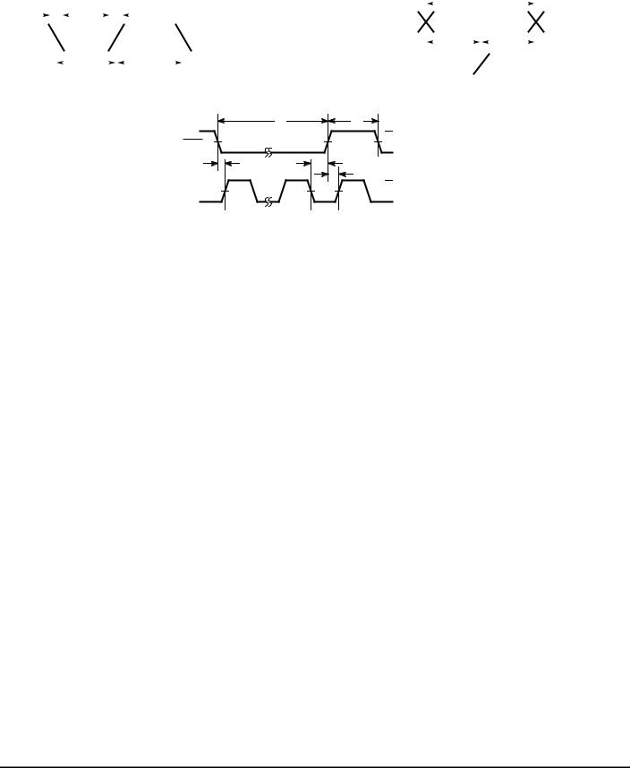
Pulse Width, Data Clock |
(Figure 1) |
tw |
5 |
|
50 |
— |
— |
ns |
|||
|
|
|
|
|
|
|
3 |
|
100 |
— |
— |
|
|
|
|
|
|
|
|
|
|
|
|||
|
DCLK Rise/Fall Time |
(Figure 1) |
tr, tf |
5 |
|
— |
— |
20 |
μs |
|||
|
|
|
|
|
|
|
3 |
|
— |
— |
120 |
|
|
|
|
|
|
|
|
|
|
|
|||
|
Setup Time, Din to DCLK |
(Figure 2) |
tsu |
5 |
|
0 |
— |
— |
ns |
|||
|
|
|
|
|
|
|
3 |
|
0 |
— |
— |
|
|
|
|
|
|
|
|
|
|
|
|||
|
Hold Time, Din to DCLK |
(Figure 2) |
th |
5 |
|
30 |
— |
— |
ns |
|||
|
|
|
|
|
|
|
3 |
|
60 |
— |
— |
|
|
|
|
|
|
|
|
|
|
|
|
|
|
|
DCLK Low to |
|
High |
(Figure 3) |
th |
5 |
|
10 |
— |
— |
ns |
|
ENB |
|
|||||||||||
|
|
|
|
|
|
|
3 |
|
20 |
— |
— |
|
|
|
|
|
|
|
|
|
|
|
|
||
|
|
High to DCLK High |
(Figure 3) |
trec |
5 |
|
10 |
— |
— |
ns |
||
|
ENB |
|
||||||||||
|
|
|
|
|
|
|
3 |
|
20 |
— |
— |
|
|
|
|
|
|
|
|
|
|
|
|
||
|
|
High Pulse Width |
(Figure 3) |
tw |
5 |
|
50 |
— |
— |
ns |
||
|
ENB |
|
||||||||||
|
|
|
|
|
|
|
3 |
|
100 |
— |
— |
|
|
|
|
|
|
|
|
|
|
|
|
||
|
|
Low to DCLK High |
(Figure 3) |
tsu |
5 |
|
10 |
— |
— |
ns |
||
|
ENB |
|
||||||||||
|
|
|
|
|
|
|
3 |
|
20 |
— |
— |
|
|
|
|
|
|
|
|
|
|
|
|
|
|
NOTE: Timing for Figures 1, 2, and 3 are design estimates only.
*For a time (t = 4/OSC FREQ.) after the backplane waveform changes to a new voltage level, the circuit is maintained in the high-current state to allow the load capacitances to charge quickly. The circuit is then returned to the low-current state until the next voltage change.
MOTOROLA |
MC14LC5003 • MC14LC5004 |
3–5
SWITCHING WAVEFORMS
|
|
|
|
|
|
|
|
|
|
tf |
|
|
|
|
|
|
|
|
|
|
|
|
tr |
|
|
|
|
|
|
|
|
|
|
|
|
|
|
|
|
|
|
|
|
VALID |
|
|
|
|
|
|
|
|
|
VDD |
||||||||
|
|
|
|
|
|
|
|
|
|
|
|
|
|
|
|
|
|
|
|
|
|
|
|
|
|
|
|
|
|
|
|
|
|
|
|
|
|
|
|
|
|
|
|
|
|
|
|
|
|
|
||||||||||||
|
|
|
|
|
|
|
|
|
|
|
|
|
|
|
|
|
|
|
|
|
|
|
|
|
|
|
|
|
Din |
|
|
|
50% |
|
|
|
|
|
|
|
|
|
|
|
|
|
|
|
|
|
||||||||||||
|
|
|
|
|
|
|
|
|
|
|
|
|
|
|
|
|
|
|
|
|
|
|
|
|
|
|
|
|
|
|
|
|
|
|
|
|
|
|
|
|
|
|
|
|
|
|
|
|
|
|
|
|
|
|||||||||
|
|
|
|
|
|
|
|
|
|
|
|
|
|
|
|
|
|
|
|
|
|
|
|
|
|
|
|
|
|
|
|
|
|
|
|
|
|
|
|
|
|
|
|
|
|
|
|
|
|
|
||||||||||||
|
|
|
|
|
|
|
|
|
|
|
|
|
|
|
|
|
|
|
|
|
|
|
|
|
|
|
|
|
|
|
|
|
|
|
|
|
|
|
|
|
|
|
|
|
|
|
|
|
|
|
||||||||||||
90% |
|
|
|
|
|
|
|
|
|
|
|
|
|
|
|
|
|
|
|
|
|
|
|
|
|
|
|
|
VDD |
|
|
|
|
|
|
|
|
|
|
|
|
|
|
|
|
|
|
|
|
|
|
|
|
|
|
|
GND |
|||||
CLK 50% |
|
|
|
|
|
|
|
|
|
|
|
|
|
|
|
|
|
|
|
|
|
|
|
|
|
|
|
GND |
|
|
|
|
|
tsu |
|
|
|
|
|
|
|
|
th |
|
|
|
|
|
|
|
|
|
||||||||||
|
|
|
|
|
|
|
|
|
|
|
|
|
|
|
|
|
|
|
|
|
|
|
|
|
|
|
|
|
|
|
|
|
|
|
|
|
|
|
|
|
|
|
|
|
|
|
|
|
|
|||||||||||||
10% |
|
|
|
|
|
|
|
|
|
|
|
|
|
|
|
|
|
|
|
|
|
|
|
|
|
|
|
|
|
|
|
|
|
|
|
|
|
|
|
|
|
|
|
|
|
|
|
|
|
|
VDD |
|||||||||||
|
|
|
|
|
|
|
|
|
|
|
|
|
|
|
|
|
|
|
|
|
|
|
|
|
|
|
|
|
|
|
|
|
|
|
|
|
|
|
|
|
|
|
|
|
|
|
|
|
|
|
|
|
|
|
|
|
|
|
|
|
|
|
|
|
|
|
|
|
|
|
|
|
|
tw |
|
|
|
|
|
|
|
|
|
|
|
|
|
tw |
|
|
|
|
|
|
|
CLK |
|
|
|
|
|
50% |
|||||||||||||||||||||||
|
|
|
|
|
|
|
|
|
|
|
|
|
|
|
|
|
|
|
|
|
|
|
|
|
|
|
|
|
|
|
|
|
|
|
|
|
|
|
|
|
|
|
|
|
|
|
|
|
GND |
|||||||||||||
|
|
|
|
|
|
|
|
|
|
|
|
|
|
|
|
|
|
|
|
|
|
|
|
|
|
|
|
|
|
|
|
|
|
|
|
|
|
|||||||||||||||||||||||||
|
|
|
|
|
|
|
|
|
|
|
|
|
|
|
|
|
|
|
|
|
|
|
|
|
|
|
|
|
|
|
|
|
|
|
|
|
|
|
|
|
|
|
|
|
|
|
|
|
|
|
|
|
|
|
|
|
|
|
|
|
|
|
|
|
|
|
|
|
|
|
|
|
|
|
|
|
|
|
|
|
|
|
|
|
|
|
|
|
|
|
|
|
|
|
|
|
|
|
|
|
|
|
|
|
|
|
|
|
|
|
|
|
|
|
|
|
|
|
|
|
|
|
|
|
|
|
|
|
|
|
|
|
|
|
|
|
|
|
|
|
|
Figure 1. |
|
|
|
|
|
|
|
|
|
|
|
|
|
|
|
|
|
|
|
|
Figure 2. |
|||||||||||||||||||||||||
|
tw |
|
tw |
|
ENB |
50% |
|
|
VDD |
|
|
GND |
||
|
tsu |
|
th |
|
|
|
|
||
|
|
|
trec |
VDD |
CLK |
50% |
|
|
|
|
|
GND |
||
|
FIRST |
LAST |
|
|
|
|
|
||
|
CLK |
CLK |
|
|
Figure 3.
MC14LC5003 • MC14LC5004 |
MOTOROLA |
3–6
FUNCTIONAL DESCRIPTION
The MC14LC5003/MC14LC5004 has essentially two sections which operate asynchronously from each other; the data input and storage section and the LCD drive section. The LCD drive and timing is derived from the oscillator, while the data input and storage is controlled by the Data In (Din), Data Clock
(DCLK), Address (A0, A1, A2), and Enable (ENB) pins. Data is shifted serially into the 128-bit shift register and ar-
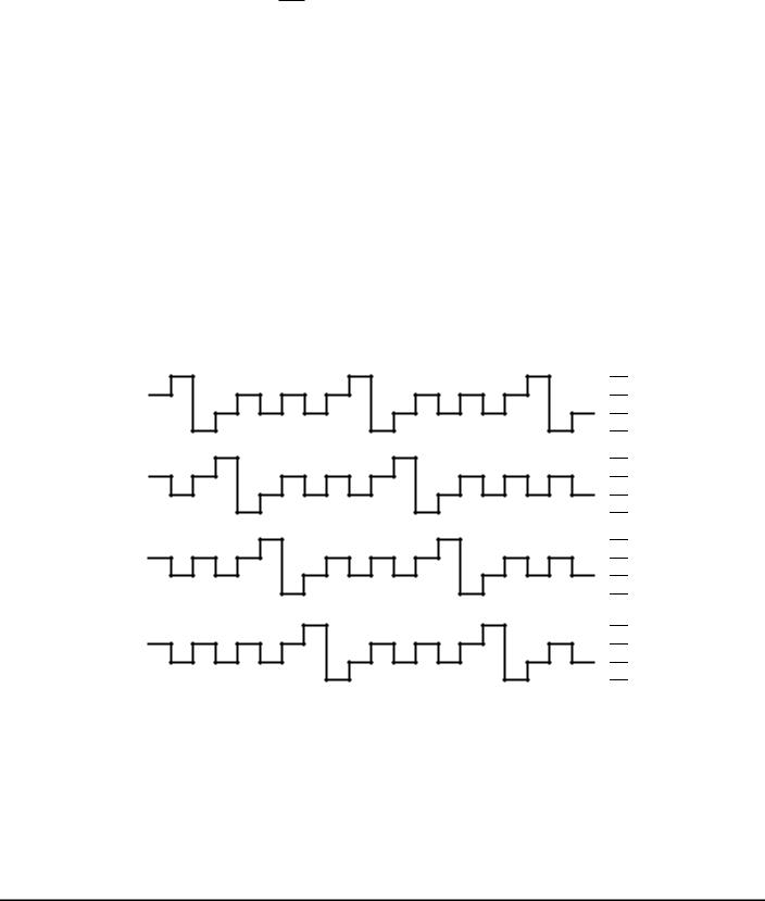
ranged into four consecutive blocks of 32 parallel data bits. A time-multiplex of the four backplane drivers is made (each backplane driver becoming active then inactive one after another) and, at the start of each backplane active period, the corresponding block of 32 bits is made available at the frontplane drivers. A high input to a plane driver turns the driver on, and a low input turns the driver off.
Figure 4 shows the sequence of backplanes. Figure 5 shows the possible configurations of the frontplanes relative to the backplanes. When a backplane driver is on, its output switches
from VLCD to 0 V, and when it is off, it switches from 1/3 VLCD to 2/3 VLCD. When a frontplane driver is on, its
output switches from 0 V to VLCD, and when it is off, it switches
from 2/3 VLCD to 1/3 VLCD.
The LCD drive and timing section provides the multiplex signals and backplane driver input signals and formats the frontplane and backplane waveforms.
The address pins are used to uniquely distinguish LCD driver from any other chips on the same bus and to define LCD driver as the “master” in the system. There must be one master in any system.
The enable pin may be used as a third control line in the communication bus. It may be used to define the moment when the data is latched. If not used, then the data is latched after 128 bits of data have been received.

 TIME FRAME

BP1
BP2
BP3
BP4
VLCD
2/3 (VLCD)
1/3 (VLCD) 0 V
VLCD
2/3 (VLCD) 1/3 (VLCD) 0 V
VLCD
2/3 (VLCD)
1/3 (VLCD) 0 V
VLCD
2/3 (VLCD) 1/3 (VLCD) 0 V
Figure 4. Backplane Sequence
MOTOROLA |
MC14LC5003 • MC14LC5004 |
3–7
 Loading...