


MOTOROLA MC14521BFEL, MC14521BF, MC14521BDR2, MC14521BD, MC14521BCP Datasheet
...
MC14521B
24-Stage Frequency Divider
The MC14521B consists of a chain of 24 flip±flops with an input circuit that allows three modes of operation. The input will function as a crystal oscillator, an RC oscillator, or as an input buffer for an external oscillator. Each flip±flop divides the frequency of the previous flip±flop by two, consequently this part will count up to 224 = 16,777,216. The count advances on the negative going edge of the clock. The outputs of the last seven±stages are available for added flexibility.
•All Stages are Resettable
•Reset Disables the RC Oscillator for Low Standby Power Drain
•RC and Crystal Oscillator Outputs Are Capable of Driving External Loads
•Test Mode to Reduce Test Time
•VDD′and VSS′Pins Brought Out on Crystal Oscillator Inverter to Allow the Connection of External Resistors for Low±Power Operation
•Supply Voltage Range = 3.0 Vdc to 18 Vdc
•Capable of Driving Two Low±power TTL Loads or One Low±power Schottky TTL Load over the Rated Temperature Range.
MAXIMUM RATINGS (Voltages Referenced to VSS) (Note 2.)
Symbol |
Parameter |
Value |
Unit |
|
|
|
|
VDD |
DC Supply Voltage Range |
± 0.5 to +18.0 |
V |
Vin, Vout |
Input or Output Voltage Range |
± 0.5 to VDD + 0.5 |
V |
|
(DC or Transient) |
|
|
|
|
|
|
Iin, Iout |
Input or Output Current |
± 10 |
mA |
|
(DC or Transient) per Pin |
|
|
|
|
|
|
PD |
Power Dissipation, |
500 |
mW |
|
per Package (Note 3.) |
|
|
|
|
|
|
TA |
Ambient Temperature Range |
± 55 to +125 |
°C |
Tstg |
Storage Temperature Range |
± 65 to +150 |
°C |
TL |
Lead Temperature |
260 |
°C |
|
(8±Second Soldering) |
|
|
|
|
|
|
2.Maximum Ratings are those values beyond which damage to the device may occur.
3.Temperature Derating:
Plastic ªP and D/DWº Packages: ± 7.0 mW/C From 65_C To 125_C
This device contains protection circuitry to guard against damage due to high static voltages or electric fields. However, precautions must be taken to avoid applications of any voltage higher than maximum rated voltages to this high±impedance circuit. For proper operation, Vin and Vout should be constrained
to the range VSS v (Vin or Vout) v VDD.
Unused inputs must always be tied to an appropriate logic voltage level (e.g., either VSS or VDD). Unused outputs must be left open.
http://onsemi.com
|
|
MARKING |
|
|
DIAGRAMS |
|
|
16 |
|
PDIP±16 |
MC14521BCP |
|
P SUFFIX |
|
|
AWLYYWW |
|
|
CASE 648 |
|
|
|
|
|
|
1 |
|
|
16 |
|
SOIC±16 |
14521B |
|
D SUFFIX |
|
|
AWLYWW |
|
|
CASE 751B |
|
|
|
|
|
|
1 |
|
|
16 |
|
SOEIAJ±16 |
MC14521B |
|
F SUFFIX |
|
|
AWLYWW |
|
|
CASE 966 |
|
|
|
|
|
|
1 |
A |
= Assembly Location |
|
WL or L = Wafer Lot |
|
|
YY or Y |
= Year |
|
WW or W = Work Week |
||
ORDERING INFORMATION |
||
Device |
Package |
Shipping |
MC14521BCP |
PDIP±16 |
2000/Box |
MC14521BD |
SOIC±16 |
48/Rail |
MC14521BDR2 |
SOIC±16 |
2500/Tape & Reel |
MC14521BF |
SOEIAJ±16 |
See Note 1. |
MC14521BFEL |
SOEIAJ±16 |
See Note 1. |
MC14521BFR2 |
SOEIAJ±16 |
See Note 1. |
1.For ordering information on the EIAJ version of the SOIC packages, please contact your local ON Semiconductor representative.
Semiconductor Components Industries, LLC, 2000 |
1 |
Publication Order Number: |
March, 2000 ± Rev. 3 |
|
MC14521B/D |
MC14521B
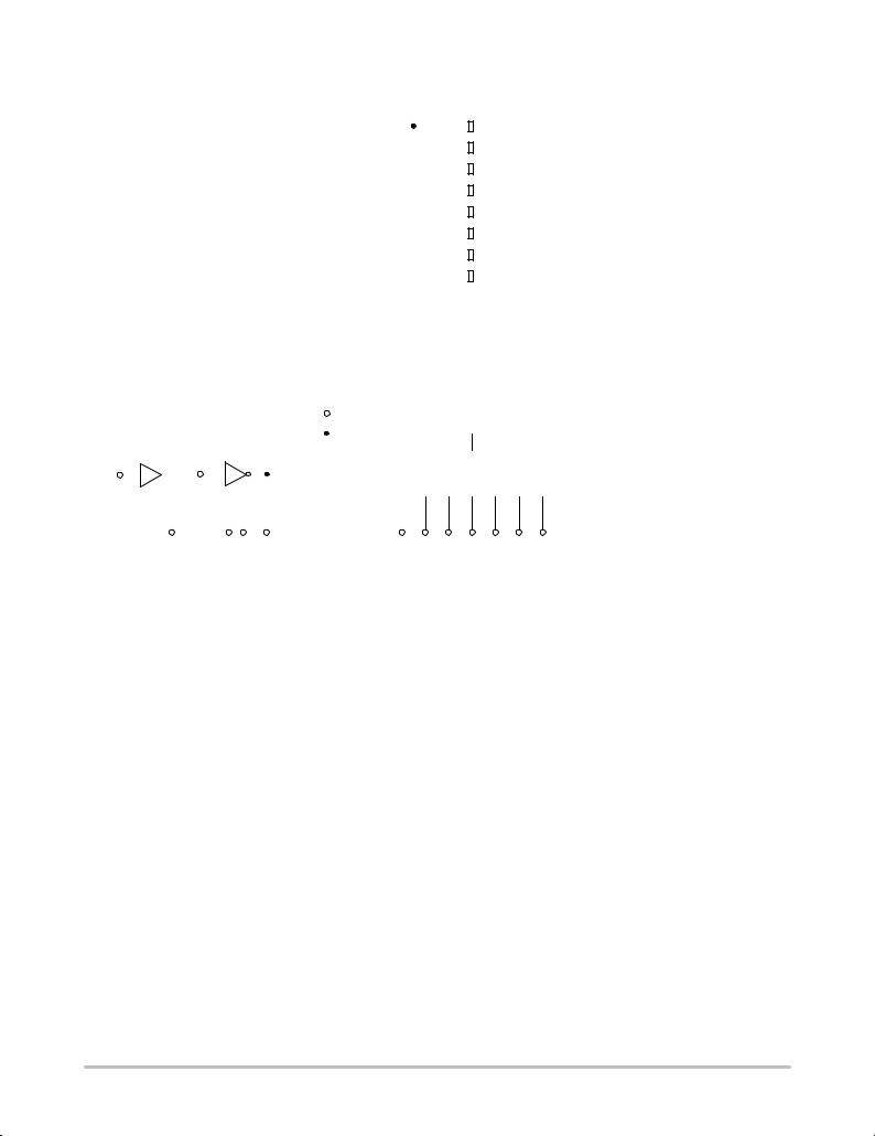
PIN ASSIGNMENT
Q24 |
|
1 |
16 |
VDD |
|
||||
|
||||
RESET |
|
2 |
15 |
Q23 |
VSS′ |
|
3 |
14 |
Q22 |
|
||||
|
||||
OUT 2 |
|
4 |
13 |
Q21 |
|
||||
VDD′ |
|
5 |
12 |
Q20 |
|
||||
|
||||
IN 2 |
|
6 |
11 |
Q19 |
|
||||
|
|
7 |
10 |
Q18 |
|
|
|||
VSS |
|
8 |
9 |
IN 1 |
|
||||
|
BLOCK DIAGRAM
RESET 2
|
|
|
|
|
|
|
|
|
|
|
|
|
|
|
|
|
|
|
Output |
Count Capacity |
|
|
|
|
|
|
|
|
|
|
|
|
|
|
|
|
|
|
|
|
|
|
|
|
|
|
|
|
|
|
|
|
|
|
|
|
|
|
|
|
|
|
Q18 |
218 |
= 262,144 |
|
|
|
|
|
|
|
|
|
|
|
STAGES |
|
|
STAGES |
|
|
Q19 |
219 |
= 524,288 |
||
9 |
|
|
|
6 |
|
|
|
|
|
|
|
|
|
|
Q20 |
220 |
= 1,048,576 |
||||
|
|
|
|
|
|
|
|
|
1 THRU 17 |
|
|
18 THRU 24 |
|
|
|||||||
|
|
|
|
|
|
|
|
|
|
|
|
|
Q21 |
221 |
= 2,097,152 |
||||||
IN 1 |
|
IN 2 |
|
|
|
|
|
|
|
|
Q18 Q19 Q20 Q21 Q22 Q23 |
Q24 |
|
||||||||
|
|
|
|
|
|
|
|
|
|
Q22 |
222 |
= 4,194,304 |
|||||||||
|
|
|
|
|
|
|
|
|
|
|
VDD = PIN 16 |
|
|
|
|
|
|
||||
|
|
|
|
|
|
|
|
|
|
|
|
|
|
|
|
|
Q23 |
23 |
= 8,388,608 |
||
|
|
|
|
|
|
|
|
|
|
|
VSS = PIN 8 |
|
|
|
|
|
|
2 |
|||
|
|
|
|
5 |
|
|
|
|
4 |
|
|
|
|
|
|
Q24 |
224 |
= 16,777,216 |
|||
7 |
|
VDD′ |
3 |
OUT2 |
10 11 12 13 14 15 |
1 |
|
|
|
|
|||||||||||
|
|
|
|||||||||||||||||||
|
|
OUT 1 |
VSS′ |
|
|
|
|
|
|
|
|
|
|
|
|
|
|||||
http://onsemi.com
2

MC14521B
ELECTRICAL CHARACTERISTICS (Voltages Referenced to VSS)
|
|
|
VDD |
± 55_C |
|
25_C |
|
|
125_C |
|
||
|
|
|
|
|
|
|
|
|
|
|
|
|
Characteristic |
Symbol |
Vdc |
Min |
Max |
Min |
Typ (4.) |
Max |
Min |
Max |
Unit |
||
Output Voltage |
ª0º Level |
VOL |
5.0 |
Ð |
0.05 |
Ð |
0 |
0.05 |
Ð |
0.05 |
Vdc |
|
Vin = VDD or 0 |
|
|
10 |
Ð |
0.05 |
Ð |
0 |
0.05 |
Ð |
0.05 |
|
|
|
|
|
15 |
Ð |
0.05 |
Ð |
0 |
0.05 |
Ð |
0.05 |
|
|
|
|
|
|
|
|
|
|
|
|
|
|
|
|
ª1º Level |
VOH |
5.0 |
4.95 |
Ð |
4.95 |
5.0 |
Ð |
4.95 |
Ð |
Vdc |
|
Vin = 0 or VDD |
|
|
10 |
9.95 |
Ð |
9.95 |
10 |
Ð |
9.95 |
Ð |
|
|
|
|
|
15 |
14.95 |
Ð |
14.95 |
15 |
Ð |
14.95 |
Ð |
|
|
|
|
|
|
|
|
|
|
|
|
|
|
|
Input Voltage |
ª0º Level |
VIL |
|
|
|
|
|
|
|
|
|
Vdc |
(VO = 4.5 or 0.5 Vdc) |
|
5.0 |
Ð |
1.5 |
Ð |
2.25 |
1.5 |
Ð |
1.5 |
|
||
(VO = 9.0 or 1.0 Vdc) |
|
10 |
Ð |
3.0 |
Ð |
4.50 |
3.0 |
Ð |
3.0 |
|
||
(VO = 13.5 or 1.5 Vdc) |
|
15 |
Ð |
4.0 |
Ð |
6.75 |
4.0 |
Ð |
4.0 |
|
||
|
ª1º Level |
VIH |
|
|
|
|
|
|
|
|
|
Vdc |
(VO = 0.5 or 4.5 Vdc) |
|
5.0 |
3.5 |
Ð |
3.5 |
2.75 |
Ð |
3.5 |
Ð |
|
||
(VO = 1.0 or 9.0 Vdc) |
|
10 |
7.0 |
Ð |
7.0 |
5.50 |
Ð |
7.0 |
Ð |
|
||
(VO = 1.5 or 13.5 Vdc) |
|
15 |
11 |
Ð |
11 |
8.25 |
Ð |
11 |
Ð |
|
||
Output Drive Current |
|
IOH |
|
|
|
|
|
|
|
|
|
mAdc |
(VOH = 2.5 Vdc) |
Source |
|
5.0 |
± 1.2 |
Ð |
± 1.0 |
± 1.7 |
Ð |
± 0.7 |
Ð |
|
|
(VOH = 4.6 Vdc) |
Pins 4 & 7 |
|
5.0 |
± 0.25 |
Ð |
± 0.2 |
± 0.36 |
Ð |
± 0.14 |
Ð |
|
|
(VOH = 9.5 Vdc) |
|
|
10 |
± 0.62 |
Ð |
± 0.5 |
± 0.9 |
Ð |
± 0.35 |
Ð |
|
|
(VOH = 13.5 Vdc) |
|
|
15 |
± 1.8 |
Ð |
± 1.5 |
± 3.5 |
Ð |
± 1.1 |
Ð |
|
|
(VOH = 2.5 Vdc) |
Source |
|
5.0 |
± 3.0 |
Ð |
± 2.4 |
± 4.2 |
Ð |
± 1.7 |
Ð |
mAdc |
|
(VOH = 4.6 Vdc) |
Pins 1, 10, |
|
5.0 |
± 0.64 |
Ð |
± 0.51 |
± 0.88 |
Ð |
± 0.36 |
Ð |
|
|
(VOH = 9.5 Vdc) |
11, 12, 13, 14 |
|
10 |
± 1.6 |
Ð |
± 1.3 |
± 2.25 |
Ð |
± 0.9 |
Ð |
|
|
(VOH = 13.5 Vdc) |
and 15 |
|
15 |
± 4.2 |
Ð |
± 3.4 |
± 8.8 |
Ð |
± 2.4 |
Ð |
|
|
(VOL = 0.4 Vdc) |
Sink |
|
|
|
|
|
|
|
|
|
|
|
I |
5.0 |
0.64 |
Ð |
0.51 |
0.88 |
Ð |
0.36 |
Ð |
mAdc |
|||
(VOL = 0.5 Vdc) |
|
OL |
10 |
1.6 |
Ð |
1.3 |
2.25 |
Ð |
0.9 |
Ð |
|
|
|
|
|
||||||||||
(VOL = 1.5 Vdc) |
|
|
15 |
4.2 |
Ð |
3.4 |
8.8 |
Ð |
2.4 |
Ð |
|
|
Input Current |
|
Iin |
15 |
Ð |
± 0.1 |
Ð |
± 0.00001 |
± 0.1 |
Ð |
± 1.0 |
μAdc |
|
Input Capacitance |
|
Cin |
Ð |
Ð |
Ð |
Ð |
5.0 |
7.5 |
Ð |
Ð |
pF |
|
(Vin = 0) |
|
|
|
|
|
|
|
|
|
|
|
|
Quiescent Current |
|
IDD |
5.0 |
Ð |
5.0 |
Ð |
0.005 |
5.0 |
Ð |
150 |
μAdc |
|
(Per Package) |
|
|
10 |
Ð |
10 |
Ð |
0.010 |
10 |
Ð |
300 |
|
|
|
|
|
15 |
Ð |
20 |
Ð |
0.015 |
20 |
Ð |
600 |
|
|
|
|
|
|
|
|
|
|
|
|
|
|
|
Total Supply Current (5.) (6.) |
I |
5.0 |
|
|
I = (0.42 μA/kHz) f + I |
DD |
|
|
μAdc |
|||
|
|
T |
|
|
|
T |
|
|
|
|
|
|
(Dynamic plus Quiescent, |
|
10 |
|
|
IT = (0.85 μA/kHz) f + IDD |
|
|
|
||||
Per Package) |
|
|
15 |
|
|
IT = (1.40 μA/kHz) f + IDD |
|
|
|
|||
(CL = 50 pF on all outputs, all |
|
|
|
|
|
|
|
|
|
|
|
|
buffers switching) |
|
|
|
|
|
|
|
|
|
|
|
|
|
|
|
|
|
|
|
|
|
|
|
|
|
4.Data labelled ªTypº is not to be used for design purposes but is intended as an indication of the IC's potential performance.
5.The formulas given are for the typical characteristics only at 25_C.
6.To calculate total supply current at loads other than 50 pF:
IT(CL) = IT(50 pF) + (CL ± 50) Vfk
where: IT is in μA (per package), CL in pF, V = (VDD ± VSS) in volts, f in kHz is input frequency, and k = 0.003.
http://onsemi.com
3
MC14521B
SWITCHING CHARACTERISTICS (7.) (CL = 50 pF, TA = 25_C)
|
|
VDD |
|
Typ (8.) |
|
|
Characteristic |
Symbol |
Vdc |
Min |
Max |
Unit |
|
|
|
|
|
|
|
|
Output Rise and Fall Time (Counter Outputs) |
tTLH, tTHL |
|
|
|
|
ns |
tTLH, tTHL = (1.5 ns/pF) CL + 25 ns |
|
5.0 |
Ð |
100 |
200 |
|
tTLH, tTHL = (0.75 ns/pF) CL + 12.5 ns |
|
10 |
Ð |
50 |
100 |
|
tTLH, tTHL = (0.55 ns/pF) CL + 12.5 ns |
|
15 |
Ð |
40 |
80 |
|
Propagation Delay Time |
tPHL, tPLH |
|
|
|
|
μs |
Clock to Q18 |
|
|
|
|
|
|
tPHL, tPLH = (1.7 ns/pF) CL + 4415 ns |
|
5.0 |
Ð |
4.5 |
9.0 |
|
tPHL, tPLH = (0.66 ns/pF) CL + 1667 ns |
|
10 |
Ð |
1.7 |
3.5 |
|
tPHL, tPLH = (0.5 ns/pF) CL + 1275 ns |
|
15 |
Ð |
1.3 |
2.7 |
|
Clock to Q24 |
|
|
|
|
|
|
tPHL, tPLH = (1.7 ns/pF) CL + 5915 ns |
|
5.0 |
Ð |
6.0 |
12 |
|
tPHL, tPLH = (0.66 ns/pF) CL + 2167 ns |
|
10 |
Ð |
2.2 |
4.5 |
|
tPHL, tPLH = (0.5 ns/pF) CL + 1675 ns |
|
15 |
Ð |
1.7 |
3.5 |
|
Propagation Delay Time |
tPHL |
|
|
|
|
ns |
Reset to Qn |
|
|
|
|
|
|
tPHL = (1.7 ns/pF) CL + 1215 ns |
|
5.0 |
Ð |
1300 |
2600 |
|
tPHL = (0.66 ns/pF) CL + 467 ns |
|
10 |
Ð |
500 |
1000 |
|
tPHL = (0.5 ns/pF) CL + 350 ns |
|
15 |
Ð |
375 |
750 |
|
Clock Pulse Width |
tWH(cl) |
5.0 |
385 |
140 |
Ð |
ns |
|
|
10 |
150 |
55 |
Ð |
|
|
|
15 |
120 |
40 |
Ð |
|
|
|
|
|
|
|
|
Clock Pulse Frequency |
fcl |
5.0 |
Ð |
3.5 |
2.0 |
MHz |
|
|
10 |
Ð |
9.0 |
5.0 |
|
|
|
15 |
Ð |
12 |
6.5 |
|
|
|
|
|
|
|
|
Clock Rise and Fall Time |
tTLH, tTHL |
5.0 |
Ð |
Ð |
15 |
μs |
|
|
10 |
Ð |
Ð |
5.0 |
|
|
|
15 |
Ð |
Ð |
4.0 |
|
|
|
|
|
|
|
|
Reset Pulse Width |
tWH(R) |
5.0 |
1400 |
700 |
Ð |
ns |
|
|
10 |
600 |
300 |
Ð |
|
|
|
15 |
450 |
225 |
Ð |
|
|
|
|
|
|
|
|
Reset Removal Time |
trem |
5.0 |
30 |
± 200 |
Ð |
ns |
|
|
10 |
0 |
± 160 |
Ð |
|
|
|
15 |
± 40 |
± 110 |
Ð |
|
|
|
|
|
|
|
|
7.The formulas given are for the typical characteristics only at 25_C.
8.Data labelled ªTypº is not to be used for design purposes but is intended as an indication of the IC's potential performance.
|
VDD |
|
|
|
|
|
500 μF |
ID |
|
0.01 μF |
|
|
|
|
CERAMIC |
|
|
|||
|
|
|
|
|
||
|
VDD |
VDD |
|
|
|
|
PULSE |
|
Q18 |
|
20 ns |
20 ns |
|
IN 2 |
CL |
90% |
VDD |
|||
Q19 |
||||||
GENERATOR |
||||||
|
Q20 |
CL |
Vin |
50% |
||
|
|
CL |
10% |
0 V |
||
|
|
Q21 |
50% DUTY CYCLE |
|||
|
|
CL |
||||
|
|
Q22 |
||||
|
|
|
|
|||
|
R |
Q23 |
CL |
|
|
|
|
Q24 |
CL |
|
|
||
|
|
|
|
|||
|
VSS |
VSS |
CL |
|
|
|
|
|
|
|
|||
Figure 1. Power Dissipation Test Circuit and Waveform
http://onsemi.com
4
 Loading...