


MC1416BP
SEMICONDUCTOR
TECHNICAL DATA
PERIPHERAL
DRIVER ARRAYS
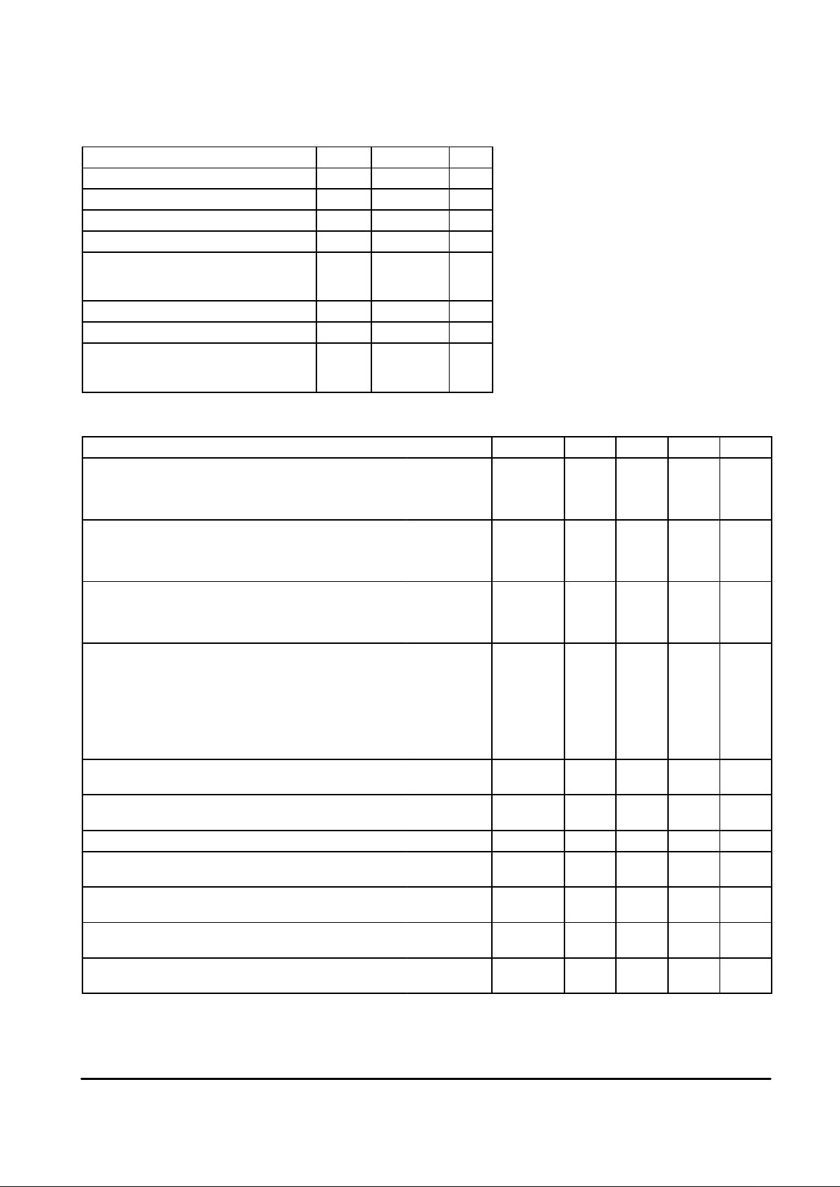
PIN CONNECTIONS
Order this document by MC1413/D
P SUFFIX
PLASTIC PACKAGE
CASE 648
D SUFFIX
PLASTIC PACKAGE
CASE 751B
(SO–16)
9
10
11
12
13
14
15
16
8
7
6
5
4
3
2
1
16
1
16
1
(Top View)
1
MOTOROLA ANALOG IC DEVICE DATA
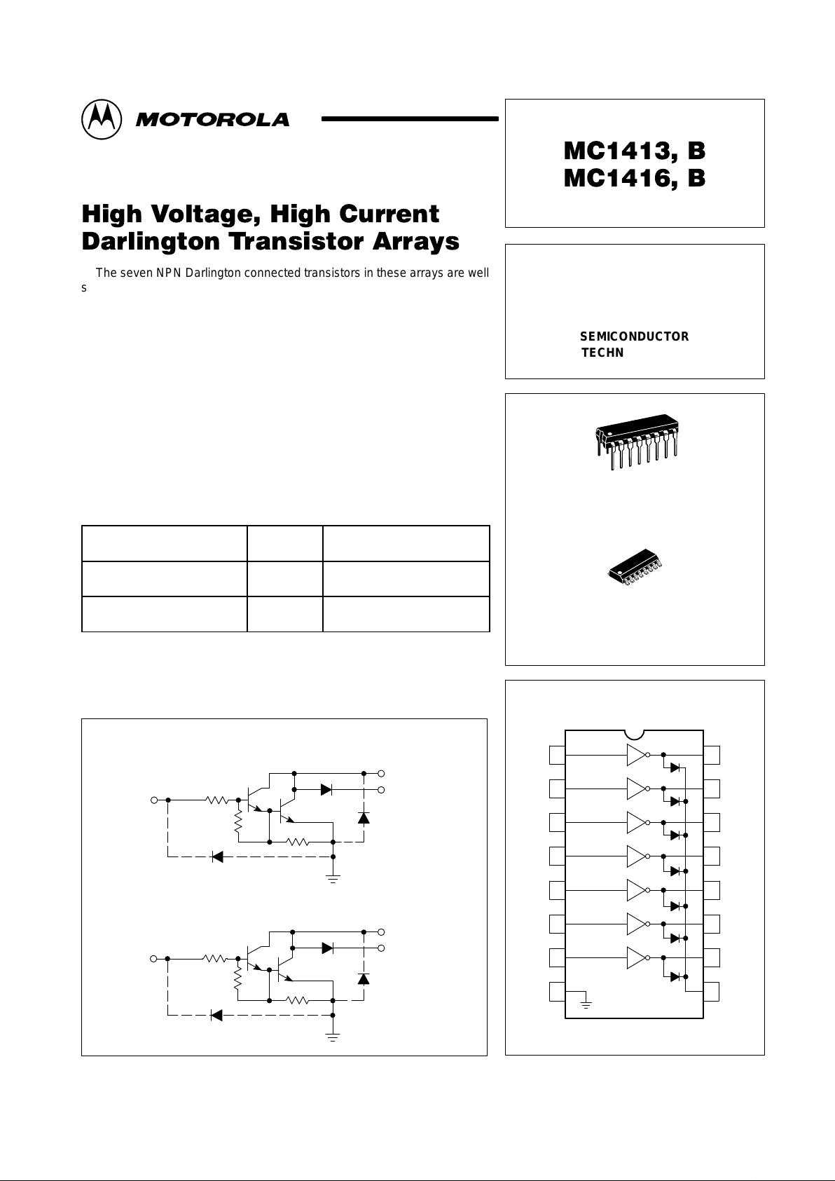
The seven NPN Darlington connected transistors in these arrays are well
suited for driving lamps, relays, or printer hammers in a variety of industrial
and consumer applications. Their high breakdown voltage and internal
suppression diodes insure freedom from problems associated with inductive
loads. Peak inrush currents to 500 mA permit them to drive incandescent
lamps.
The MC1413, B with a 2.7 kΩ series input resistor is well suited for
systems utilizing a 5.0 V TTL or CMOS Logic. The MC1416, B uses a series
10.5 kΩ resistor and is useful in 8.0 to 18 V MOS systems.
ORDERING INFORMATION
Plastic DIP SOIC
Operating
Temperature Range
MC1413P (ULN2003A)
MC1416P (ULN2004A)
MC1413D
MC1416D
T
A
= –20° to +85°C
MC1413BP
MC1416BP
MC1413BD
MC1416BD
T
A
= –40° to +85°C
Representative Schematic Diagrams
5.0 k
10.5 k
5.0 k
3.0 k
Pin 9
Pin 9
3.0 k
1/7 MC1413, B
2.7 k
1/7 MC1416, B
Motorola, Inc. 1996 Rev 0
MC1413, B MC1416, B
2
MOTOROLA ANALOG IC DEVICE DATA
MAXIMUM RATINGS
(T
A
= 25°C, and rating apply to any one device in the
package, unless otherwise noted.)
Rating
Symbol Value Unit
Output Voltage V
O
50 V
Input Voltage V
I
30 V
Collector Current – Continuous I
C
500 mA
Base Current – Continuous I
B
25 mA
Operating Ambient Temperature Range
MC1413–16
MC1413B–16B
T
A
–20 to +85
–40 to +85
°C
Storage Temperature Range T
stg
–55 to +150 °C
Junction Temperature T
J
150 °C
Thermal Resistance, Junction–to–Ambient
Case 648, P Suffix
Case 751B, D Suffix
θ
JA
67
100
°C/W
NOTE: ESD data available upon request.
ELECTRICAL CHARACTERISTICS (T
A
= 25°C, unless otherwise noted)
Characteristic Symbol Min Typ Max Unit
Output Leakage Current
(V
O
= 50 V, T
A
= +85°C)
(V
O
= 50 V, T
A
= +25°C)
(V
O
= 50 V, T
A
= +85°C, V
I
= 1.0 V)
All Types
All Types
MC1416, B
I
CEX
–
–
–
–
–
–
100
50
500
µA
Collector–Emitter Saturation Voltage
(I
C
= 350 mA, I
B
= 500 µA)
(I
C
= 200 mA, I
B
= 350 µA)
(I
C
= 100 mA, I
B
= 250 µA)
All Types
All Types
All Types
V
CE(sat)
–
–
–
1.1
0.95
0.85
1.6
1.3
1.1
V
Input Current – On Condition
(V
I
= 3.85 V)
(V
I
= 5.0 V)
(V
I
= 12 V)
MC1413, B
MC1416, B
MC1416, B
I
I(on)
–
–
–
0.93
0.35
1.0
1.35
0.5
1.45
mA
Input Voltage – On Condition
(V
CE
= 2.0 V , I
C
= 200 mA)
(V
CE
= 2.0 V , I
C
= 250 mA)
(V
CE
= 2.0 V , I
C
= 300 mA)
(V
CE
= 2.0 V , I
C
= 125 mA)
(V
CE
= 2.0 V , I
C
= 200 mA)
(V
CE
= 2.0 V , I
C
= 275 mA)
(V
CE
= 2.0 V , I
C
= 350 mA)
MC1413, B
MC1413, B
MC1413, B
MC1416, B
MC1416, B
MC1416, B
MC1416, B
V
I(on)
–
–
–
–
–
–
–
–
–
–
–
–
–
–
2.4
2.7
3.0
5.0
6.0
7.0
8.0
V
Input Current – Off Condition
(I
C
= 500 µA, T
A
= 85°C)
All Types I
I(off)
50 100 – µA
DC Current Gain
(V
CE
= 2.0 V , I
C
= 350 mA)
h
FE
1000 – – –
Input Capacitance C
I
– 15 30 pF
Turn–On Delay Time
(50% E
I
to 50% E
O
)
t
on
– 0.25 1.0 µs
Turn–Off Delay Time
(50% E
I
to 50% E
O
)
t
off
– 0.25 1.0 µs
Clamp Diode Leakage Current
(V
R
= 50 V)
T
A
= +25°C
T
A
= +85°C
I
R
–
–
–
–
50
100
µA
Clamp Diode Forward Voltage
(I
F
= 350 mA)
V
F
– 1.5 2.0 V
 Loading...