


MC14599BCL
MOTOROLA CMOS LOGIC DATAMC14099B MC14599B
246
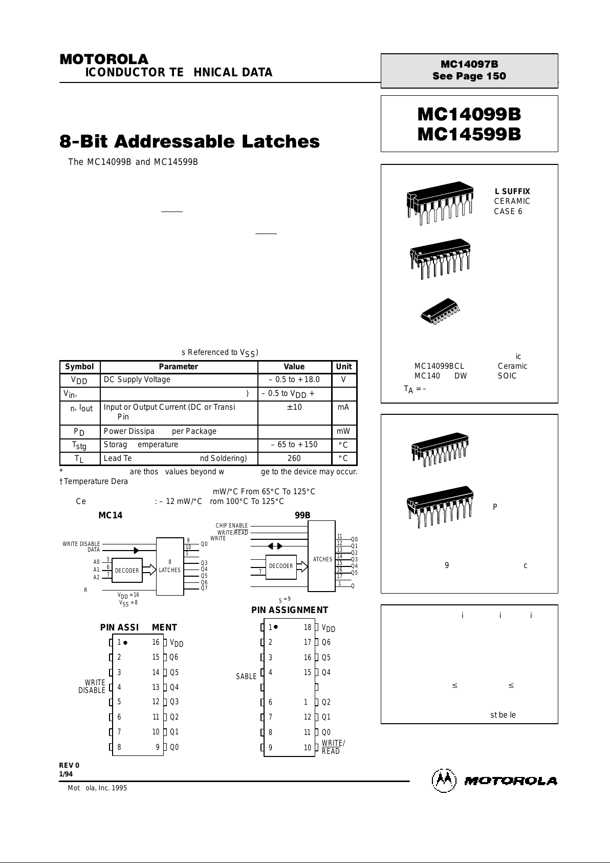
The MC14099B and MC14599B are 8–bit addressable latches. Data is
entered in serial form when the appropriate latch is addressed (via address
pins A0, A1, A2) and write disable is in the low state. Chip enable must be
high for w riting into MC14599B. F or the MC14599B the data pin is a
bidirectional data port and for the MC14099B the input is a unidirectional
write only port. The Write/Read
line controls this port in the MC14599B.
The d ata is p resented in p arallel a t the output of t he eight latches
independently of the state of Write Disable, Write/Read
or Chip Enable.
A Master Reset capability is available on both parts.
• Serial Data Input
• Parallel Output
• Master Reset
• Supply Voltage Range = 3.0 Vdc to 18 Vdc
• Capable of Driving Two Low–power TTL Loads or One Low–Power
Schottky TTL Load over the Rated Temperature Range
• MC14099B pin for pin compatible with CD4099B
MAXIMUM RATINGS* (Voltages Referenced to V
SS
)
Symbol
Parameter
Value
Unit
V
DD
DC Supply Voltage
– 0.5 to + 18.0
V
V
in
, V
out
Input or Output Voltage (DC or Transient)
– 0.5 to V
DD
+ 0.5
V
I
in
, I
out
Input or Output Current (DC or Transient),
per Pin
± 10
mA
P
D
Power Dissipation, per Package†
500
mW
T
stg
Storage Temperature
– 65 to + 150
_
C
T
L
Lead Temperature (8–Second Soldering)
260
_
C
*Maximum Ratings are those values beyond which damage to the device may occur.
†Temperature Derating:
Plastic “P and D/DW” Packages: – 7.0 mW/
_
C From 65
_
C To 125
_
C
Ceramic “L” Packages: – 12 mW/
_
C From 100
_
C To 125
_
C
MC14099B MC14599B
13
14
15
16
9
10
11
125
4
3
2
1
8
7
6
Q3
Q4
Q5
Q6
V
DD
Q0
Q1
Q2
WRITE
DISABLE
DATA
RESET
Q7
V
SS
A2
A1
A0
A0
DATA
RESET
Q7
V
SS
CE
A2
A1
WRITE
DISABLE
Q4
Q5
Q6
V
DD
WRITE/
READ
Q0
Q1
Q2
Q3
14
15
16
17
18
10
11
12
13
5
4
3
2
1
9
8
7
6
PIN ASSIGNMENT
PIN ASSIGNMENT
CHIP ENABLE
WRITE/READ
WRITE DISABLE
DATA
A0
A1
A2
RESET
8
10
4
3
2
5
6
7
DECODER
11
12
13
14
15
16
17
1
Q7
Q6
Q5
Q4
Q3
Q2
Q1
Q0
8
LATCHES
Q7
Q6
Q5
Q4
Q3
Q2
Q1
Q0
8
LATCHES
DECODER
5
6
7
WRITE DISABLE
DATA
A0
A1
A2
RESET
8
4
3
2
8
V
DD
= 18
V
SS
= 9
V
DD
= 16
V
SS
= 8
9
10
11
12
13
14
15
1
SEMICONDUCTOR TECHNICAL DATA
Motorola, Inc. 1995
REV 0
1/94
L SUFFIX
CERAMIC
CASE 620
ORDERING INFORMATION
MC14099BCP Plastic
MC14099BCL Ceramic
MC14099BDW SOIC
T
A
= – 55° to 125°C for all packages.
P SUFFIX
PLASTIC
CASE 648
DW SUFFIX
SOIC
CASE 751G
L SUFFIX
CERAMIC
CASE 726
ORDERING INFORMATION
MC14599BCP Plastic
MC14599BCL Ceramic
P SUFFIX
PLASTIC
CASE 707
This device contains protection circuitry to
guard against damage due to high static
voltages or electric fields. However, pre-
cautions must be taken to avoid applications of
any voltage higher than maximum rated volt-
ages to this high–impedance circuit. For proper
operation, V
in
and V
out
should be constrained
to the range V
SS
v
(V
in
or V
out
)
v
V
DD
.
Unused inputs must always be tied to an
appropriate logic voltage level (e.g., either V
SS
or V
DD
). Unused outputs must be left open.
T
A
= – 55° to 125°C for all packages.
MOTOROLA CMOS LOGIC DATA
247
MC14099B MC14599B
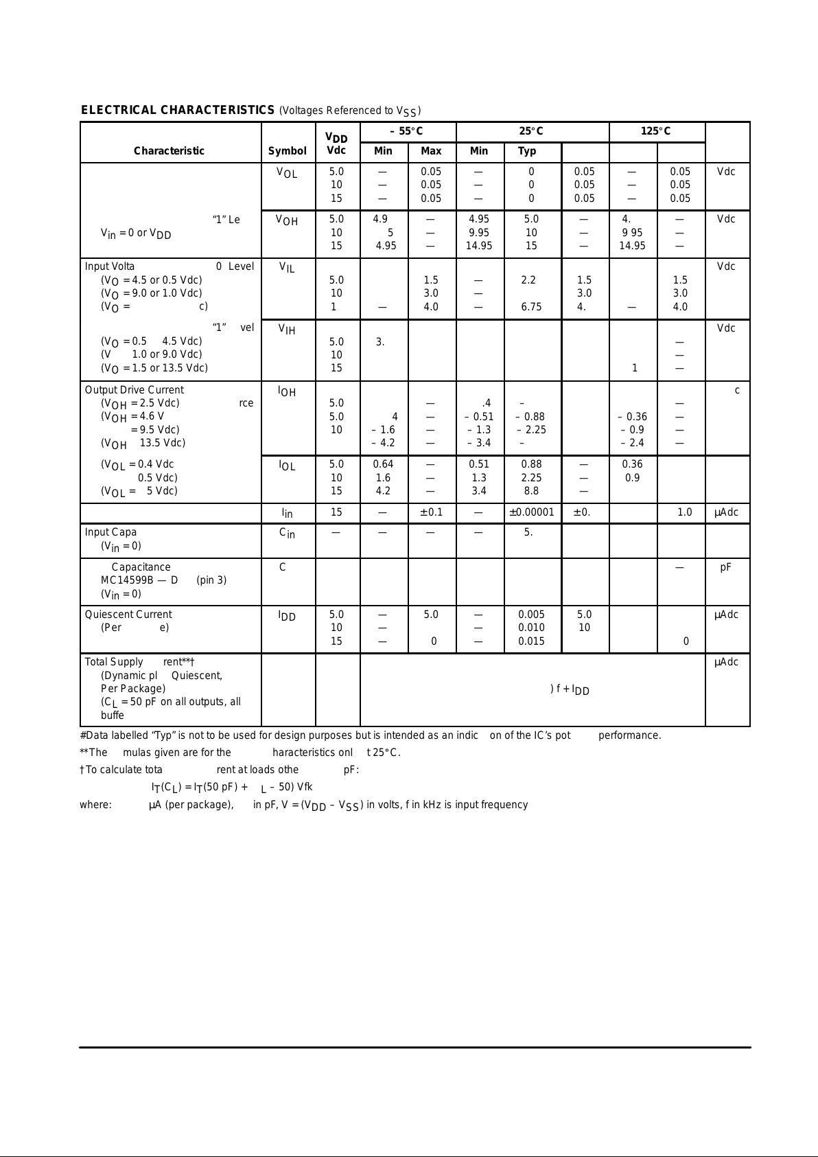
ELECTRICAL CHARACTERISTICS (Voltages Referenced to V
SS
)
V
– 55
_
C
25
_
C
125
_
C
Characteristic
Symbol
V
DD
Vdc
Min
Max
Min
Typ #
Max
Min
ÎÎÎ
ÎÎÎ
ÎÎÎ
Max
Unit
Output Voltage
“0” Level
V
in
= V
DD
or 0
V
OL
5.0
10
15
—
—
—
0.05
0.05
0.05
—
—
—
0
0
0
0.05
0.05
0.05
—
—
—
ÎÎÎ
ÎÎÎ
ÎÎÎ
ÎÎÎ
0.05
0.05
0.05
Vdc
“1” Level
V
in
= 0 or V
DD
V
OH
5.0
10
15
4.95
9.95
14.95
—
—
—
4.95
9.95
14.95
5.0
10
15
—
—
—
4.95
9.95
14.95
ÎÎÎ
ÎÎÎ
ÎÎÎ
ÎÎÎ
ÎÎÎ
—
—
—
Vdc
Input Voltage
“0” Level
(V
O
= 4.5 or 0.5 Vdc)
(V
O
= 9.0 or 1.0 Vdc)
(V
O
= 13.5 or 1.5 Vdc)
V
IL
5.0
10
15
—
—
—
1.5
3.0
4.0
—
—
—
2.25
4.50
6.75
1.5
3.0
4.0
—
—
—
ÎÎÎ
ÎÎÎ
ÎÎÎ
ÎÎÎ
ÎÎÎ
1.5
3.0
4.0
Vdc
“1” Level
(V
O
= 0.5 or 4.5 Vdc)
(V
O
= 1.0 or 9.0 Vdc)
(V
O
= 1.5 or 13.5 Vdc)
V
IH
5.0
10
15
3.5
7.0
11
—
—
—
3.5
7.0
11
2.75
5.50
8.25
—
—
—
3.5
7.0
11
ÎÎÎ
ÎÎÎ
ÎÎÎ
ÎÎÎ
ÎÎÎ
—
—
—
Vdc
Output Drive Current
(V
OH
= 2.5 Vdc) Source
(V
OH
= 4.6 Vdc)
(V
OH
= 9.5 Vdc)
(V
OH
= 13.5 Vdc)
I
OH
5.0
5.0
10
15
– 3.0
– 0.64
– 1.6
– 4.2
—
—
—
—
– 2.4
– 0.51
– 1.3
– 3.4
– 4.2
– 0.88
– 2.25
– 8.8
—
—
—
—
– 1.7
– 0.36
– 0.9
– 2.4
ÎÎÎ
ÎÎÎ
ÎÎÎ
ÎÎÎ
ÎÎÎ
—
—
—
—
mAdc
(V
OL
= 0.4 Vdc) Sink
(V
OL
= 0.5 Vdc)
(V
OL
= 1.5 Vdc)
I
OL
5.0
10
15
0.64
1.6
4.2
—
—
—
0.51
1.3
3.4
0.88
2.25
8.8
—
—
—
0.36
0.9
2.4
ÎÎÎ
ÎÎÎ
ÎÎÎ
ÎÎÎ
ÎÎÎ
—
—
—
mAdc
Input Current
I
in
15
—
± 0.1
—
±0.00001
± 0.1
—
ÎÎÎ
ÎÎÎ
ÎÎÎ
± 1.0
µAdc
Input Capacitance
(V
in
= 0)
C
in
—
—
—
—
5.0
7.5
—
ÎÎÎ
ÎÎÎ
ÎÎÎ
—
pF
Input Capacitance
MC14599B — Data (pin 3)
(V
in
= 0)
C
in
—
—
—
—
15
22.5
—
ÎÎÎ
ÎÎÎ
ÎÎÎ
ÎÎÎ
ÎÎÎ
—
pF
Quiescent Current
(Per Package)
I
DD
5.0
10
15
—
—
—
5.0
10
20
—
—
—
0.005
0.010
0.015
5.0
10
20
—
—
—
ÎÎÎ
ÎÎÎ
ÎÎÎ
ÎÎÎ
150
300
600
µAdc
Total Supply Current**†
(Dynamic plus Quiescent,
Per Package)
(C
L
= 50 pF on all outputs, all
buffers switching)
I
T
5.0
10
15
I
T
= (1.5 µA/kHz) f + I
DD
I
T
= (3.0 µA/kHz) f + I
DD
I
T
= (4.5 µA/kHz) f + I
DD
µAdc
#Data labelled “Typ” is not to be used for design purposes but is intended as an indication of the IC’s potential performance.
**The formulas given are for the typical characteristics only at 25
_
C.
†To calculate total supply current at loads other than 50 pF:
I
T
(C
L
) = I
T
(50 pF) + (C
L
– 50) Vfk
where: I
T
is in µA (per package), C
L
in pF, V = (V
DD
– V
SS
) in volts, f in kHz is input frequency, and k = 0.004.

MOTOROLA CMOS LOGIC DATAMC14099B MC14599B
248
SWITCHING CHARACTERISTICS* (C
L
= 50 pF, T
A
= 25
_
C)
Characteristic
ÎÎÎÎ
ÎÎÎÎ
ÎÎÎÎ
ÎÎÎÎ
Symbol
V
DD
Vdc
ÎÎÎÎ
ÎÎÎÎ
ÎÎÎÎ
ÎÎÎÎ
Min
Typ #
Max
Unit
Output Rise and Fall Time
t
TLH
, t
THL
= (1.35 ns/pF) C
L
+ 32 ns
t
TLH
, t
THL
= (0.6 ns/pF) C
L
+ 20 ns
t
TLH
, t
THL
= (0.4 ns/pF) C
L
+ 20 ns
ÎÎÎÎ
ÎÎÎÎ
ÎÎÎÎ
ÎÎÎÎ
ÎÎÎÎ
t
TLH
,
t
THL
5.0
10
15
ÎÎÎÎ
ÎÎÎÎ
ÎÎÎÎ
ÎÎÎÎ
ÎÎÎÎ
—
—
—
100
50
40
200
100
80
ns
Propagation Delay Time
Data to Output Q
ÎÎÎÎ
ÎÎÎÎ
ÎÎÎÎ
ÎÎÎÎ
ÎÎÎÎ
t
PHL
,
t
PLH
5.0
10
15
ÎÎÎÎ
ÎÎÎÎ
ÎÎÎÎ
ÎÎÎÎ
ÎÎÎÎ
—
—
—
200
75
50
400
150
100
ns
Write Disable to Output Q
ÎÎÎÎ
ÎÎÎÎ
ÎÎÎÎ
ÎÎÎÎ
5.0
10
15
ÎÎÎÎ
ÎÎÎÎ
ÎÎÎÎ
ÎÎÎÎ
—
—
—
200
80
60
400
160
120
ns
Reset to Output Q
ÎÎÎÎ
ÎÎÎÎ
ÎÎÎÎ
ÎÎÎÎ
5.0
10
15
ÎÎÎÎ
ÎÎÎÎ
ÎÎÎÎ
ÎÎÎÎ
—
—
—
175
80
65
350
160
130
ns
CE to Output Q (MC14599B only)
ÎÎÎÎ
ÎÎÎÎ
ÎÎÎÎ
ÎÎÎÎ
ÎÎÎÎ
5.0
10
15
ÎÎÎÎ
ÎÎÎÎ
ÎÎÎÎ
ÎÎÎÎ
ÎÎÎÎ
—
—
—
225
100
75
450
200
150
ns
Propagation Delay Time, MC14599B only
Chip Enable, Write/Read
to Data
ÎÎÎÎ
ÎÎÎÎ
ÎÎÎÎ
ÎÎÎÎ
t
PHL
,
t
PLH
5.0
10
15
ÎÎÎÎ
ÎÎÎÎ
ÎÎÎÎ
ÎÎÎÎ
—
—
—
200
80
65
400
160
130
ns
Address to Data
ÎÎÎÎ
ÎÎÎÎ
ÎÎÎÎ
ÎÎÎÎ
ÎÎÎÎ
5.0
10
15
ÎÎÎÎ
ÎÎÎÎ
ÎÎÎÎ
ÎÎÎÎ
ÎÎÎÎ
—
—
—
200
90
75
400
180
150
ns
Pulse Widths
Reset
ÎÎÎÎ
ÎÎÎÎ
ÎÎÎÎ
ÎÎÎÎ
ÎÎÎÎ
t
w(H)
t
w(L)
5.0
10
15
ÎÎÎÎ
ÎÎÎÎ
ÎÎÎÎ
ÎÎÎÎ
ÎÎÎÎ
150
75
50
75
40
25
—
—
—
ns
Write Disable
ÎÎÎÎ
ÎÎÎÎ
ÎÎÎÎ
ÎÎÎÎ
5.0
10
15
ÎÎÎÎ
ÎÎÎÎ
ÎÎÎÎ
ÎÎÎÎ
320
160
120
160
80
60
—
—
—
ns
Set Up Time
Data to Write Disable
ÎÎÎÎ
ÎÎÎÎ
ÎÎÎÎ
ÎÎÎÎ
ÎÎÎÎ
t
su
5.0
10
15
ÎÎÎÎ
ÎÎÎÎ
ÎÎÎÎ
ÎÎÎÎ
ÎÎÎÎ
100
50
35
50
25
20
—
—
—
ns
Hold Time
Write Disable to Data
ÎÎÎÎ
ÎÎÎÎ
ÎÎÎÎ
ÎÎÎÎ
ÎÎÎÎ
t
h
5.0
10
15
ÎÎÎÎ
ÎÎÎÎ
ÎÎÎÎ
ÎÎÎÎ
ÎÎÎÎ
150
75
50
75
40
25
—
—
—
ns
Set Up Time
Address to Write Disable
ÎÎÎÎ
ÎÎÎÎ
ÎÎÎÎ
ÎÎÎÎ
t
su
5.0
10
15
ÎÎÎÎ
ÎÎÎÎ
ÎÎÎÎ
ÎÎÎÎ
100
80
40
45
30
10
—
—
—
ns
Removal Time
Write Disable to Address
ÎÎÎÎ
ÎÎÎÎ
ÎÎÎÎ
ÎÎÎÎ
ÎÎÎÎ
t
rem
5.0
10
15
ÎÎÎÎ
ÎÎÎÎ
ÎÎÎÎ
ÎÎÎÎ
ÎÎÎÎ
0
0
0
– 80
– 40
– 40
—
—
—
ns
*The formulas given are for the typical characteristics only at 25
_
C.
#Data labelled “Typ” is not to be used for design purposes but is intended as an indication of the IC’s potential performance.
 Loading...