


MC14538BCP
MOTOROLA MC14538BCP, MC14538BD, MC14538BDR2, MC14538BDT, MC14538BDTR2 Datasheet
...
Semiconductor Components Industries, LLC, 2000
March, 2000 – Rev. 3
1 Publication Order Number:
MC14538B/D
MC14538B
Dual Precision
Retriggerable/Resettable
Monostable Multivibrator
The MC14538B is a dual, retriggerable, resettable monostable
multivibrator. It may be triggered from either edge of an input pulse,
and produces an accurate output pulse over a wide range of widths, the
duration and accuracy of which are determined by the external timing
components, C
X
and R
X
.
Output Pulse Width = (Cx) (Rx) where:
Rx is in k
W
Cx is in
m
F
• Unlimited Rise and Fall Time Allowed on the A Trigger Input
• Pulse Width Range = 10 µs to 10 s
• Latched Trigger Inputs
• Separate Latched Reset Inputs
• 3.0 Vdc to 18 Vdc Operational Limits
• Triggerable from Positive (A Input) or Negative–Going Edge
(B–Input)
• Capable of Driving Two Low–power TTL Loads or One Low–power
Schottky TTL Load Over the Rated Temperature Range
• Pin–for–pin Compatible with MC14528B and CD4528B (CD4098)
• Use the MC54/74HC4538A for Pulse Widths Less Than 10 µs with
Supplies Up to 6 V.
MAXIMUM RATINGS (Voltages Referenced to V
SS
) (Note 2.)
Symbol Parameter Value Unit
V
DD
DC Supply Voltage Range –0.5 to +18.0 V
V
in
, V
out
Input or Output Voltage Range
(DC or Transient)
–0.5 to V
DD
+ 0.5 V
I
in
, I
out
Input or Output Current
(DC or Transient) per Pin
±10 mA
P
D
Power Dissipation,
per Package (Note 3.)
500 mW
T
A
Operating Temperature Range –55 to +125 °C
T
stg
Storage Temperature Range –65 to +150 °C
T
L
Lead Temperature
(8–Second Soldering)
260 °C
2. Maximum Ratings are those values beyond which damage to the device
may occur.
3. Temperature Derating:
Plastic “P and D/DW” Packages: – 7.0 mW/
_
C From 65
_
C T o 125
_
C
This device contains protection circuitry to guard against damage due to high
static voltages or electric fields. However, precautions must be taken to avoid
applications of any voltage higher than maximum rated voltages to this
high–impedance circuit. For proper operation, V
in
and V
out
should be constrained
to the range V
SS
v
(V
in
or V
out
)
v
V
DD
.
Unused inputs must always be tied to an appropriate logic voltage level (e.g.,
either V
SS
or V
DD
). Unused outputs must be left open.
http://onsemi.com
A = Assembly Location
WL or L = Wafer Lot
YY or Y = Year
WW or W = Work Week
Device Package Shipping
ORDERING INFORMATION
MC14538BCP PDIP–16 2000/Box
MC14538BD SOIC–16 48/Rail
MARKING
DIAGRAMS
1
16
PDIP–16
P SUFFIX
CASE 648
MC14538BCP
AWLYYWW
MC14538BDR2 SOIC–16 2500/Tape & Reel
SOIC–16
DW SUFFIX
CASE 751G
1
16
14538B
AWLYYWW
1. For ordering information on the EIAJ version of
the SOIC packages, please contact your local
ON Semiconductor representative.
SOEIAJ–16
F SUFFIX
CASE 966
1
16
MC14538B
AWLYWW
MC14538BDT TSSOP–16 96/Rail
SOIC–16
D SUFFIX
CASE 751B
1
16
14538B
AWLYWW
TSSOP–16
DT SUFFIX
CASE 948F
14
538B
ALYW
1
16
MC14538BDTR2 TSSOP–16 2500/Tape & Reel
MC14538BDW SOIC–16 47/Rail
MC14538BDWR2 SOIC–16 1000/Tape & Reel
MC14538BF SOEIAJ–16 See Note 1.
MC14538BFEL SOEIAJ–16 See Note 1.
MC14538B
http://onsemi.com
2
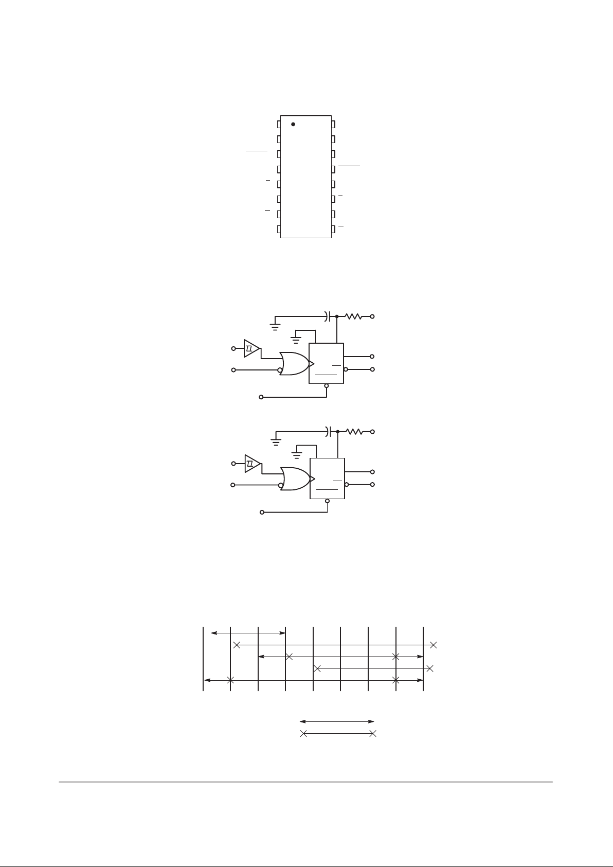
PIN ASSIGNMENT
13
14
15
16
9
10
11
125
4
3
2
1
8
7
6
A
B
RESET B
C
X
/R
X
B
V
SS
V
DD
Q
B
Q
B
B
B
A
A
RESET A
C
X
/R
X
A
V
SS
V
SS
Q
A
Q
A
B
A
BLOCK DIAGRAM
V
DD
V
DD
6
7
10
9
12
11
5
4
A
B
C
X
R
X
12
Q1
Q1
RESET
3
C
X
R
X
15 14
Q2
Q2
RESET
13
A
B
R
X
AND C
X
ARE EXTERNAL COMPONENTS.
V
DD
= PIN 16
V
SS
= PIN 8, PIN 1, PIN 15
ONE–SHOT SELECTION GUIDE
100 ns
MC14528B
MC14536B
MC14538B
MC14541B
MC4538A*
1 µs 10 µs 100 µs 1 ms 10 ms 100 ms 1 s 10 s
*LIMITED OPERATING VOLTAGE (2 – 6 V)
TOTAL OUTPUT PULSE WIDTH RANGE
RECOMMENDED PULSE WIDTH RANGE
23 HR
5 MIN.
MC14538B
http://onsemi.com
3
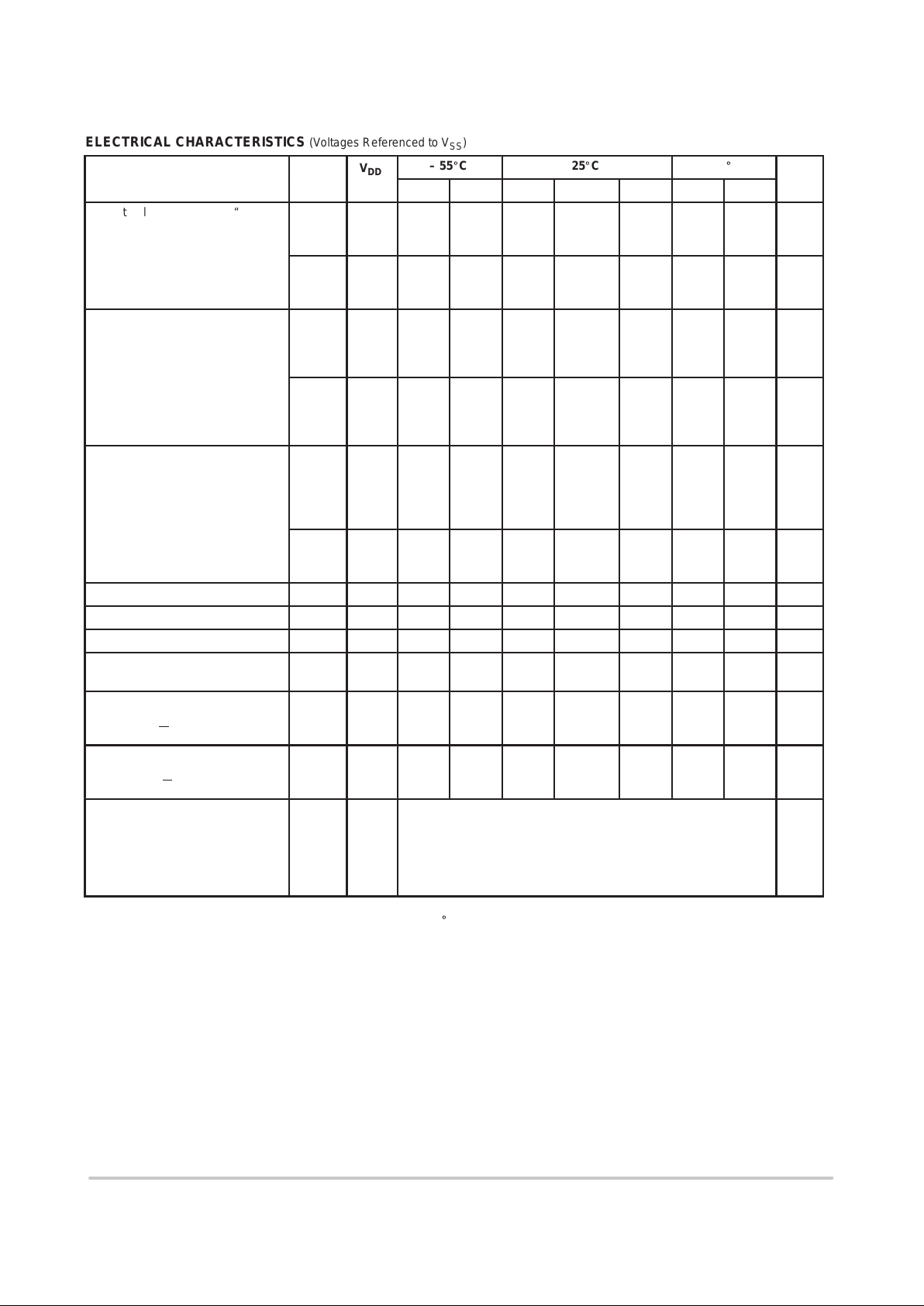
ELECTRICAL CHARACTERISTICS (Voltages Referenced to V
SS
)
V
DD
– 55
_
C 25
_
C 125
_
C
Characteristic Symbol
Vdc
Min Max Min Typ
(4.)
Max Min Max
Unit
Output Voltage “0” Level
V
in
= V
DD
or 0
V
OL
5.0
10
15
—
—
—
0.05
0.05
0.05
—
—
—
0
0
0
0.05
0.05
0.05
—
—
—
0.05
0.05
0.05
Vdc
“1” Level
V
in
= 0 or V
DD
V
OH
5.0
10
15
4.95
9.95
14.95
—
—
—
4.95
9.95
14.95
5.0
10
15
—
—
—
4.95
9.95
14.95
—
—
—
Vdc
Input Voltage “0” Level
(V
O
= 4.5 or 0.5 Vdc)
(V
O
= 9.0 or 1.0 Vdc)
(V
O
= 13.5 or 1.5 Vdc)
V
IL
5.0
10
15
—
—
—
1.5
3.0
4.0
—
—
—
2.25
4.50
6.75
1.5
3.0
4.0
—
—
—
1.5
3.0
4.0
Vdc
“1” Level
(V
O
= 0.5 or 4.5 Vdc)
(V
O
= 1.0 or 9.0 Vdc)
(V
O
= 1.5 or 13.5 Vdc)
V
IH
5.0
10
15
3.5
7.0
11
—
—
—
3.5
7.0
11
2.75
5.50
8.25
—
—
—
3.5
7.0
11
—
—
—
Vdc
Output Drive Current
(V
OH
= 2.5 Vdc) Source
(V
OH
= 4.6 Vdc)
(V
OH
= 9.5 Vdc)
(V
OH
= 13.5 Vdc)
I
OH
5.0
5.0
10
15
– 3.0
– 0.64
– 1.6
– 4.2
—
—
—
—
– 2.4
– 0.51
– 1.3
– 3.4
– 4.2
– 0.88
– 2.25
– 8.8
—
—
—
—
– 1.7
– 0.36
– 0.9
– 2.4
—
—
—
—
mAdc
(V
OL
= 0.4 Vdc) Sink
(V
OL
= 0.5 Vdc)
(V
OL
= 1.5 Vdc)
I
OL
5.0
10
15
0.64
1.6
4.2
—
—
—
0.51
1.3
3.4
0.88
2.25
8.8
—
—
—
0.36
0.9
2.4
—
—
—
mAdc
Input Current, Pin 2 or 14 I
in
15 — ±0.05 — ±0.00001 ±0.05 — ±0.5 µAdc
Input Current, Other Inputs I
in
15 — ±0.1 — ±0.00001 ±0.1 — ±1.0 µAdc
Input Capacitance, Pin 2 or 14 C
in
— — — — 25 — — — pF
Input Capacitance, Other Inputs
(V
in
= 0)
C
in
— — — — 5.0 7.5 — — pF
Quiescent Current
(Per Package)
Q = Low, Q
= High
I
DD
5.0
10
15
—
—
—
5.0
10
20
—
—
—
0.005
0.010
0.015
5.0
10
20
—
—
—
150
300
600
µAdc
Quiescent Current, Active State
(Both) (Per Package)
Q = High, Q
= Low
I
DD
5.0
10
15
—
—
—
2.0
2.0
2.0
—
—
—
0.04
0.08
0.13
0.20
0.45
0.70
—
—
—
2.0
2.0
2.0
mAdc
Total Supply Current at an external
load capacitance (C
L
) and at
external timing network (R
X
, C
X
)
(5.)
I
T
5.0
10
I
T
= (3.5 x 10
–2
) R
X
C
X
f + 4C
X
f + 1 x 10
–5
C
L
f
I
T
= (8.0 x 10
–2
) R
X
C
X
f + 9C
X
f + 2 x 10
–5
C
L
f
I
T
= (1.25 x 10
–1
) R
X
C
X
f + 12C
X
f + 3 x 10
–5
C
L
f
where: I
T
in µA (one monostable switching only),
where: C
X
in µF, C
L
in pF, R
X
in k ohms, and
where: f in Hz is the input frequency.
µAdc
4. Data labelled “Typ” is not to be used for design purposes but is intended as an indication of the IC’s potential performance.
5. The formulas given are for the typical characteristics only at 25
_
C.
MC14538B
http://onsemi.com
4
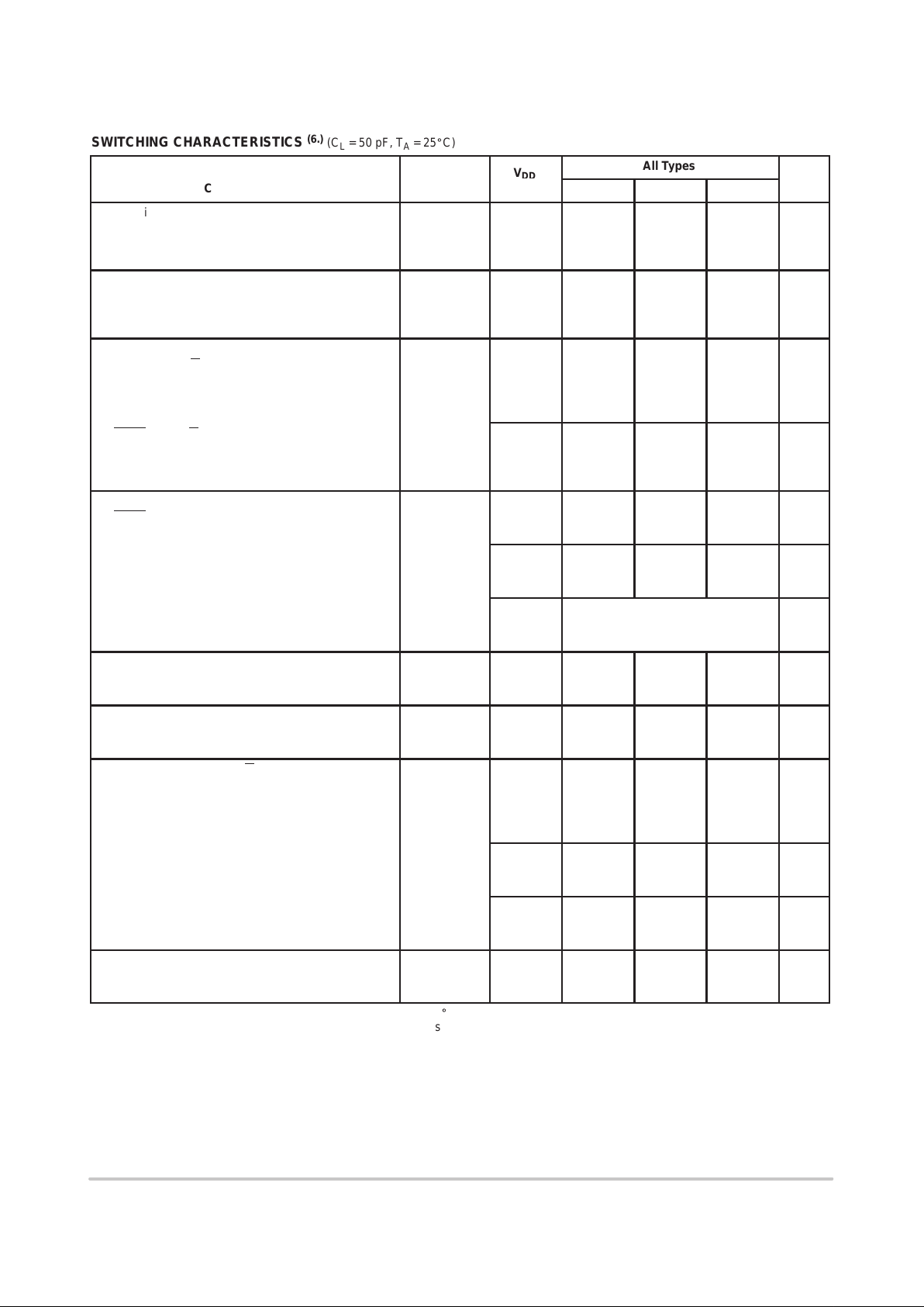
SWITCHING CHARACTERISTICS
(6.)
(C
L
= 50 pF, T
A
= 25
_
C)
V
All Types
Characteristic Symbol
V
DD
Vdc
Min Typ
(7.)
Max
Unit
Output Rise Time
t
TLH
= (1.35 ns/pF) C
L
+ 33 ns
t
TLH
= (0.60 ns/pF) C
L
+ 20 ns
t
TLH
= (0.40 ns/pF) C
L
+ 20 ns
t
TLH
5.0
10
15
—
—
—
100
50
40
200
100
80
ns
Output Fall Time
t
THL
= (1.35 ns/pF) C
L
+ 33 ns
t
THL
= (0.60 ns/pF) C
L
+ 20 ns
t
THL
= (0.40 ns/pF) C
L
+ 20 ns
t
THL
5.0
10
15
—
—
—
100
50
40
200
100
80
ns
Propagation Delay Time
A or B to Q or Q
t
PLH
, t
PHL
= (0.90 ns/pF) C
L
+ 255 ns
t
PLH
, t
PHL
= (0.36 ns/pF) C
L
+ 132 ns
t
PLH
, t
PHL
= (0.26 ns/pF) C
L
+ 87 ns
t
PLH
,
t
PHL
5.0
10
15
—
—
—
300
150
100
600
300
220
ns
Reset to Q or Q
t
PLH
, t
PHL
= (0.90 ns/pF) C
L
+ 205 ns
t
PLH
, t
PHL
= (0.36 ns/pF) C
L
+ 107 ns
t
PLH
, t
PHL
= (0.26 ns/pF) C
L
+ 82 ns
5.0
10
15
—
—
—
250
125
95
500
250
190
ns
Input Rise and Fall Times
Reset
t
r
, t
f
5
10
15
—
—
—
—
—
—
15
5
4
µs
B Input 5
10
15
—
—
—
300
1.2
0.4
1.0
0.1
0.05
ms
A Input 5
10
15
No Limit
—
Input Pulse Width
A, B, or Reset
t
WH
,
t
WL
5.0
10
15
170
90
80
85
45
40
—
—
—
ns
Retrigger Time t
rr
5.0
10
15
0
0
0
—
—
—
—
—
—
ns
Output Pulse Width — Q or Q
Refer to Figures 8 and 9
C
X
= 0.002 µF, R
X
= 100 kΩ
T
5.0
10
15
198
200
202
210
212
214
230
232
234
µs
C
X
= 0.1 µF, R
X
= 100 kΩ 5.0
10
15
9.3
9.4
9.5
9.86
10
10.14
10.5
10.6
10.7
ms
C
X
= 10 µF, R
X
= 100 kΩ 5.0
10
15
0.91
0.92
0.93
0.965
0.98
0.99
1.03
1.04
1.06
s
Pulse Width Match between circuits in
the same package.
C
X
= 0.1 µF, R
X
= 100 kΩ
100
[(T
1
– T
2
)/T
1
]
5.0
10
15
—
—
—
± 1.0
± 1.0
± 1.0
± 5.0
± 5.0
± 5.0
%
6. The formulas given are for the typical characteristics only at 25
_
C.
7. Data labelled “Typ” is not to be used for design purposes but is intended as an indication of the IC’s potential performance.
 Loading...