Motorola MC1723, RC723 Datasheet

Voltage Regulator
The MC1723C is a positive or negative voltage regulator designed to deliver load current to 150 mAdc. Output current capability can be increased to several amperes through use of one or more external pass transistors. MC1723C is specified for operation over the commercial temperature range (0° to +70°C).
•Output Voltage Adjustable from 2.0 Vdc to 37 Vdc
•Output Current to 150 mAdc Without External Pass Transistors
•0.01% Line and 0.03% Load Regulation
•Adjustable Short Circuit Protection
Order this document by MC1723C/D
MC1723C
VOLTAGE REGULATOR
SEMICONDUCTOR
TECHNICAL DATA
|
|
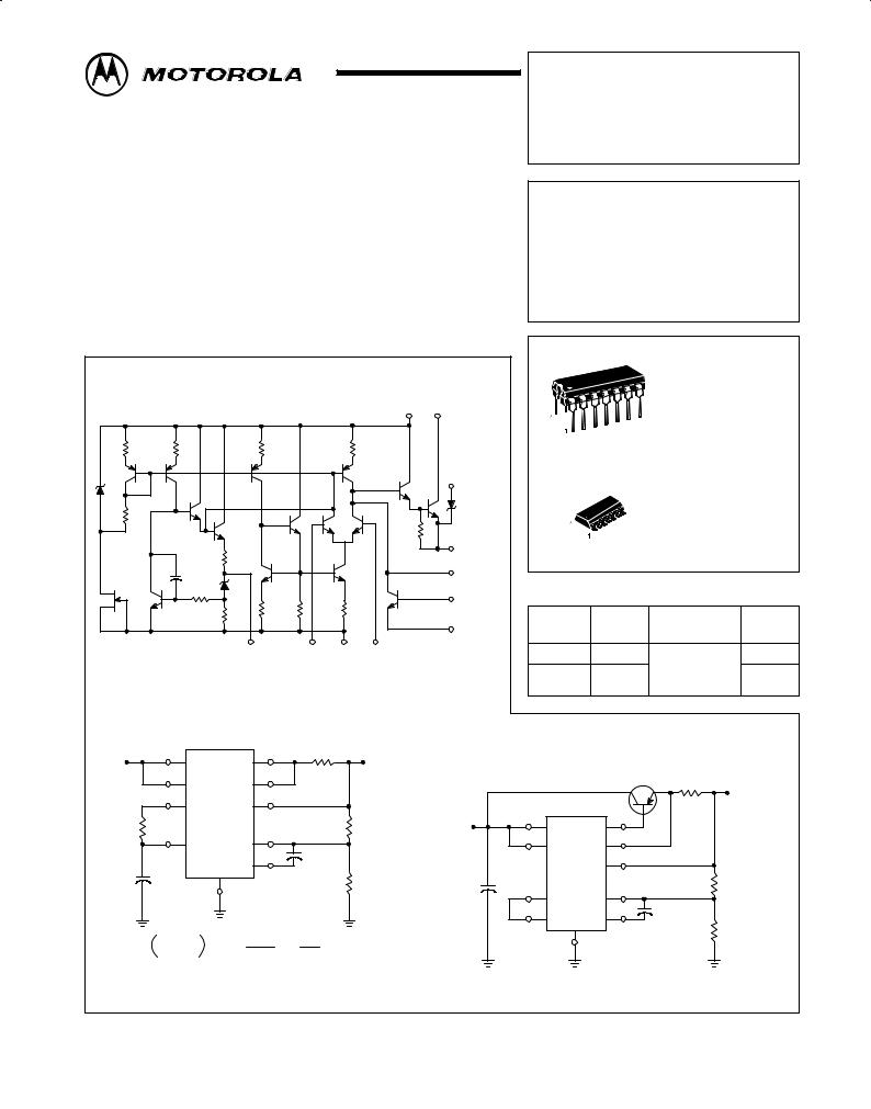
Figure 1. Representative Schematic Diagram |
|
|
|
|
|
|
P SUFFIX |
|
|
||||||||||
|
|
|
|
|
|
|
|
|
|
|
|
VCC |
V |
|
|
|
PLASTIC PACKAGE |
||||
|
|
|
|
|
|
|
|
|
|
|
|
|
|
|
|
|
CASE 646 |
|
|||
|
|
|
|
|
|
|
|
|
|
|
|
|
C |
|
|
|
|
|
|
||
|
|
|
|
|
|
|
|
|
|
|
|
12 |
11 |
|
|
|
|
|
|
|
|
|
500 |
25k |
|
|
1.0k |
|
|
|
|
1.0k |
|
|
|
|
|
|
|
|
|
|
|
6.2V |
|
|
|
|
|
|
|
|
|
|
|
|
Vz |
|
|
|
|
|
|
|
|
|
|
|
|
|
|
|
|
|
|
|
|
|
|
9 |
|
|
|
|
D SUFFIX |
|
|
|
|
|
|
|
|
|
|
|
|
|
|
|
|
6.2V |
|
|
|
|
|
|
|
|
15k |
|
|
|
|
|
|
|
|
|
|
|
|
|
|
PLASTIC PACKAGE |
|||||
|
|
|
|
|
|
|
|
|
|
|
|
|
|
|
|
|
CASE 751A |
|
|||
|
|
|
|
|
|
|
|
|
|
|
|
|
|
|
|
|
|
|
|||
|
|
|
|
|
|
|
|
|
|
|
|
15k |
10 |
|
|
|
|
|
(SO±14) |
|
|
|
|
|
|
|
|
|
|
|
|
|
|
|
VO |
|
|
|
|
|
|
|
|
|
|
|
|
100 |
|
|
|
|
|
|
|
13 |
|
|
|
|
|
|
|
||
|
|
|
|
|
|
|
|
|
|
|
Compensation |
|
|
|
|
|
|
|
|||
|
|
5.0pF |
|
|
|
|
|
|
|
|
|
|
|
|
|
|
|
|
|
||
|
|
|
6.2V |
|
|
|
|
|
|
2 Current |
|
|
|
|
|
|
|
||||
|
|
30k |
|
|
|
|
|
|
|
ORDERING INFORMATION |
|
|
|||||||||
|
|
|
5.0k |
|
300 |
|
|
|
150 |
|
|
Limit |
|
|
Operating |
|
|
||||
|
|
|
|
20k |
|
|
|
|
|
|
|
|
|
||||||||
|
|
|
|
|
|
|
|
|
|
Current |
|
|
|
|
|||||||
|
|
|
|
|
|
|
|
|
|
|
|
|
|
|
|
Temperature |
|
|
|||
|
|
|
|
|
6 |
Vref |
|
5 |
7 |
|
VEE |
4 |
3 |
Sense |
Device |
Alternate |
Range |
|
Package |
||
|
|
|
|
|
|
|
|
|
|
|
|
|
|
|
|||||||
|
|
|
|
|
|
|
Noninverting |
|
|
Inverting |
|
|
MC1723CD |
± |
|
|
|
|
SO±14 |
||
|
|
|
|
|
|
|
|
Input |
|
|
|
Input |
|
|
MC1723CP |
LM723CN |
TA = 0 |
° |
° |
Plastic DIP |
|
|
|
|
|
|
|
|
|
|
|
|
|
|
|
|
|
to +70 C |
|||||
|
|
|
|
|
|
|
|
|
|
|
|
|
|
|
|
μA723PC |
|
|
|
|
|
|
Figure 2. Typical Circuit Connection |
|
|
|
|
|
|
|
|
|
|
||||||||||
|
|
12 |
(7 < VO < 37) |
10 |
|
RSC |
|
|
|
|
Figure 3. Typical NPN Current Boost Connection |
||||||||||
Vin |
|
|
|
|
|
|
VO |
|
|
||||||||||||
|
11 |
|
|
|
2 |
|
|
|
|
|
|
|
|
|
|
|
|
|
|
||
|
|
|
|
|
|
|
|
|
|
|
|
|
|
|
RSC = 0.33 |
|
|
||||
|
|
|
|
|
|
|
|
|
|
|
|
|
|
|
|
|
|
= +15Vdc |
|||
|
|
|
|
|
|
3 |
|
|
|
|
|
|
|
|
|
|
|
|
VO |
||
|
|
|
MC1723C |
|
|
|
|
|
|
|
|
2N3055 or Equiv |
|
|
IL = 2Adc max |
||||||
|
|
6 |
|
|
|
|
|
|
|
|
|
12 |
10 |
|
|
|
|
|
|||
|
|
|
|
|
|
|
|
|
|
R1 |
Vin = 20Vdc |
|
|
|
|
|
|||||
|
R3 |
|
|
|
|
4 |
|
|
|
|
11 |
2 |
|
|
|
|
|
||||
|
|
|
|
|
|
|
|
|
|
|
|
|
|
|
|
|
|
|
|||
|
|
|
|
|
|
|
|
|
|
|
|
|
|
|
|
|
|
|
|
||
|
|
5 |
|
|
|
C1 |
|
100pF |
|
|
|
|
|
MC1723C |
3 |
|
|
|
|
|
|
|
|
|
|
|
|
|
|
|
|
|
|
|
|
|
|
|
|
|
|
|
|
|
|
Cref |
|
|
|
13 |
|
|
|
|
R2 |
|
|
0.1μF |
|
4 |
|
|
12k |
|
|
|
|
7 |
|
|
|
|
|
|
|
|
|
6 |
|
|
|
|
|||||
|
|
|
|
|
|
|
|
|
|
|
|
|
|
|
|
|
|
||||
|
|
|
|
|
|
|
|
|
|
|
|
|
|
|
5 |
C1 |
100pF |
|
|
|
|
|
|
R1 + R2 |
|
|
|
Vsense |
|
0.66 |
|
|
|
|
|
|
7 |
13 |
|
|
10k |
|
|
V |
^ 7 |
I |
SC |
= |
= |
at T |
J |
= + 25°C |
|
|
|
|
|
|
|
|
|||||
O |
|
R2 |
|
|
RSC |
|
RSC |
|
|
|
|
|
|
|
|
|
|
|
|||
|
|
|
|
|
|
|
|
|
|
|
|
|
|
|
|
|
|
||||
For best results 10 k < R2 < 100 k |
|
|
|
|
|
|
|
|
|
|
|
|
|
|
|
||||||
For minimum drift R3 = R1 | | R2 |
|
|
|
|
|
|
|
|
|
|
|
|
|
|
|
|
|||||
Motorola, Inc. 1996 |
Rev 5 |

|
MC1723C |
|
|
MAXIMUM RATINGS (TA = +25°C, unless otherwise noted.) |
|
|
|
Rating |
Symbol |
Value |
Unit |
|
|
|
|
Pulse Voltage from VCC to VEE (50 ms) |
VI(p) |
50 |
Vpk |
Continuous Voltage from VCC to VEE |
VI |
40 |
Vdc |
Input±Output Voltage Differential |
VI±VO |
40 |
Vdc |
Maximum Output Current |
IL |
150 |
mAdc |
Current from Vref |
Iref |
15 |
mAdc |
Current from Vz |
Iz |
25 |
mA |
Voltage Between Noninverting Input and VEE |
Vie |
8.0 |
Vdc |
Differential Input Voltage |
Vid |
±5.0 |
Vdc |
Power Dissipation and Thermal Characteristics |
|
|
|
TA = +25°C |
PD |
1.25 |
W |
Derate above TA = +25°C |
1/θJA |
10 |
mW/°C |
Thermal Resistance, Junction±to±Air |
θJA |
100 |
°C/W |
Operating and Storage Junction Temperature Range |
TJ, Tstg |
±65 to +175 |
°C |
Operating Ambient Temperature Range |
TA |
0 to +70 |
°C |
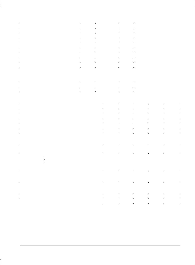
ELECTRICAL CHARACTERISTICS (TA = +25°C, Vin 12 Vdc, VO = 5.0 Vdc, IL = 1.0 mAdc, RSC = 0, C1 = 100 pF, Cref = 0 and divider impedance as seen by the error amplifier ≤ 10 kΩ connected as shown in Figure 2, unless otherwise noted.)
|
|
Characteristics |
Symbol |
Min |
Typ |
Max |
Unit |
|
|
|
|
|
|
|
|
Input Voltage Range |
|
VI |
9.5 |
± |
40 |
Vdc |
|
Output Voltage Range |
VO |
2.0 |
± |
37 |
Vdc |
||
Input±Output Voltage Differential |
VI±VO |
3.0 |
± |
38 |
Vdc |
||
Reference Voltage |
|
Vref |
6.80 |
7.15 |
7.50 |
Vdc |
|
Standby Current Drain ( IL = 0, Vin = 30 V) |
IIB |
± |
2.3 |
4.0 |
mAdc |
||
Output Noise Voltage (f = 100 Hz to 10 kHz) |
Vn |
|
|
|
μV(RMS) |
||
Cref = 0 |
|
|
± |
20 |
± |
|
|
Cref = 5.0 μF |
|
|
± |
2.5 |
± |
|
|
Average Temperature Coefficient of Output |
TCVO |
± |
0.003 |
0.015 |
%/°C |
||
Voltage (Tlow < TA < Thigh) |
|
|
|
|
|
||
Line Regulation |
12 V < Vin < 15 V |
Regline |
± |
0.01 |
0.1 |
% VO |
|
(TA = 25°C) |
|
|
|
||||
|
|
|
|||||
|
12 V < Vin < 40 V |
|
± |
0.1 |
0.5 |
|
|
|
|
|
|
||||
(Tlow < TA < Thigh) |
|
± |
± |
0.3 |
|
||
12 V < Vin < 15 V |
|
|
|||||
Load Regulation (1.0 mA < IL < 50 mA) |
Regload |
|
|
|
% VO |
||
TA = 25°C |
|
|
± |
0.03 |
0.2 |
|
|
Tlow < TA < Thigh |
|
|
± |
± |
0.6 |
|
|
Ripple Rejection (f = 50 Hz to 10 kHz) |
RR |
|
|
|
dB |
||
Cref = 0 |
|
|
± |
74 |
± |
|
|
Cref = 5.0 μF |
|
|
± |
86 |
± |
|
|
Short Circuit Current Limit (RSC = 10 Ω, VO = 0) |
ISC |
± |
65 |
± |
mAdc |
||
Long Term Stability |
|
^VO/^t |
± |
0.1 |
± |
%/1000 Hr. |
|
NOTE: Tlow to Thigh = 0° to +70°C
2 |
MOTOROLA ANALOG IC DEVICE DATA |

MC1723C
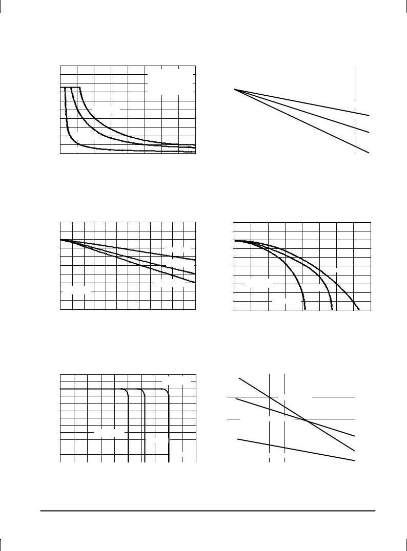
Figure 4. Maximum Load Current as a Function of Input±Output Voltage Differential
|
200 |
|
|
|
|
(mA) |
|
|
|
TJmax = 150°C |
|
160 |
|
|
RTH = 150°C/W |
|
|
CURRENT |
|
|
PSTANDBY 60 mW |
|
|
|
|
|
(No heatsink) |
|
|
120 |
|
|
|
|
|
|
TA = + 25°C |
|
|
|
|
LOAD |
|
|
|
|
|
80 |
|
|
|
|
|
(max), |
|
|
|
|
|
|
TA = + 75°C |
|
|
|
|
L |
40 |
|
|
|
|
I |
|
|
|
||
|
0 |
TA = + 125°C |
|
|
|
|
10 |
20 |
30 |
40 |
|
|
0 |
Vin±Vout, INPUT±OUTPUT VOLTAGE (V)
Figure 6. Load Regulation Characteristics
With Current Limiting
|
0.05 |
|
|
|
|
|
|
) |
|
|
|
|
|
|
|
O |
|
|
|
|
|
|
|
(%V |
0 |
|
|
|
|
|
|
REGULATION |
±0.05 |
|
|
|
|
TA = ±55°C |
|
|
|
|
|
TA = + 25°C |
|
||
|
|
|
|
|
|
||
|
|
|
|
|
|
|
|
, LOAD |
±0.1 |
|
|
|
|
|
|
|
|
|
|
|
TA = + 125°C |
|
|
load |
±0.15 |
RSC = 10 Ω |
|
|
|
|
|
Reg |
|
|
|
|
|
|
|
|
±0.2 |
5.0 |
10 |
15 |
20 |
25 |
30 |
|
0 |
IO, OUTPUT CURRENT (mA)
Figure 5. Load Regulation Characteristics
Without Current Limiting
) |
0.05 |
|
|
|
|
|
|
|
|
|
|
|
|
|
|
|
|
|
|
|
|
|
|
||
|
|
|
|
|
|
|
|
|
|
|
|
|
O |
|
|
|
|
|
|
|
|
|
|
|
|
(%V |
±0.05 |
|
|
|
|
|
|
|
|
|
|
|
|
|
|
|
|
|
|
|
|
|
|
||
REGULATION |
|
|
|
|
|
|
|
|
|
|
|
|
|
0 |
|
|
|
|
|
|
|
|
|
|
|
|
|
|
|
|
|
|
|
|
T |
A = + 25°C |
|
|
, LOAD |
|
|
|
|
|
|
|
|
TA |
= ±55°C |
|
|
|
|
|
|
|
|
|
|
|
TA = + 125°C |
|
||
load |
±0.1 |
|
|
|
|
|
|
|
|
|
||
Reg |
±0.15 |
|
|
|
|
|
|
|
|
|
|
|
|
|
|
|
|
|
|
|
|
|
|
||
|
|
|
|
|
|
|
|
|
|
|
|
|
|
|
|
|
|
|
|
|
|
|
|
|
|
|
0 |
20 |
40 |
60 |
80 |
100 |
||||||
IO, OUTPUT CURRENT (mA)
Figure 7. Load Regulation Characteristics
With Current Limiting
|
0.1 |
|
|
|
|
) |
|
|
|
|
|
O |
|
|
|
|
|
(%V |
0 |
|
|
|
|
REGULATION |
|
|
|
|
|
±0.1 |
|
|
|
|
|
|
|
|
TA = ±55°C |
|
|
, LOAD |
±0.2 |
|
|
|
|
|
|
|
|
||
|
RSC = 10 Ω |
TA = + 25°C |
|
|
|
load |
±0.3 |
|
|
|
|
|
|
|
|
||
Reg |
|
|
TA = + 125°C |
|
|
|
±0.4 |
|
|
|
|
|
0 |
20 |
40 |
60 |
80 |
|
|
|
IO, OUTPUT CURRENT (mA) |
|
|
RELATIVE OUTPUT VOLTAGE (V)
Figure 8. Current Limiting Characteristics
1.2
RSC = 10 Ω
1.0
0.8
0.6
0.4TA = + 125°C
TA=+25°C
0.2 |
|
|
|
|
|
|
|
|
|
|
|
|
TA = ±55°C |
|
|
0 |
|
|
|
|
|
|
|
|
|
|
|
|
|
|
|
|
20 |
40 |
60 |
80 |
100 |
||
0 |
|||||||
IO, OUTPUT CURRENT (mA)
CURRENT LIMIT SENSE VOLTAGE (V)
0.8
0.7
0.6
0.5
0.4
Figure 9. Current Limiting Characteristics as a Function of Junction Temperature
|
|
|
|
|
|
|
|
|
|
200 |
(mA) |
|
|
|
|
|
|
|
|
|
|
||
|
|
|
|
|
|
|
|
|
|
160 |
|
|
|
|
|
|
Sense |
Voltage |
|
|
|
||
|
|
|
|
|
|
|
|
CURRENT |
|||
|
|
|
|
|
|
|
|
|
|
|
|
|
Limit |
Current RSC = 5.0 Ω |
|
|
|
|
120 |
||||
|
|
|
|
|
LIMITING |
||||||
|
|
|
|
|
|
|
|
|
|
80 |
|
|
|
|
|
|
|
|
|
|
|
||
|
|
|
|
|
|
|
|
|
|
|
|
|
|
|
|
|
|
|
|
|
|
|
|
|
|
|
Limit Current RSC = 10 |
Ω |
|
|
|
40 |
|
||
|
|
|
|
|
|
|
|
|
|
|
|
±50 |
0 |
50 |
100 |
150 |
|
||||||
|
|
TJ, JUNCTION TEMPERATURE (°C) |
|
|
|
||||||
MOTOROLA ANALOG IC DEVICE DATA |
3 |
|
 Loading...