


MOTOROLA MC14504BFL1, MC14504BFR1, MC14504BFR2, MC14504BF, MC14504BDR2 Datasheet
...
MC14504B
Hex Level Shifter for TTL to CMOS or CMOS to CMOS
The MC14504B is a hex non±inverting level shifter using CMOS technology. The level shifter will shift a TTL signal to CMOS logic levels for any CMOS supply voltage between 5 and 15 volts. A control input also allows interface from CMOS to CMOS at one logic level to another logic level: Either up or down level translating is accomplished by selection of power supply levels VDD and VCC. The VCC level sets the input signal levels while VDD selects the output voltage levels.
•UP Translates from a Low to a High Voltage or DOWN Translates from a High to a Low Voltage
•Input Threshold Can Be Shifted for TTL Compatibility
•No Sequencing Required on Power Supplies or Inputs for Power Up or Power Down
•3 to 18 Vdc Operation for VDD and VCC
•Diode Protected Inputs to VSS
•Capable of Driving Two Low±Power TTL Loads or One Low±Power Schottky TTL Load Over the Rated Temperature Range
MAXIMUM RATINGS (Voltages Referenced to VSS) (Note 2.)
Symbol |
Parameter |
Value |
Unit |
|
|
|
|
VCC |
DC Supply Voltage Range |
± 0.5 to +18.0 |
V |
VDD |
DC Supply Voltage Range |
± 0.5 to +18.0 |
V |
Vin |
Input Voltage Range |
± 0.5 to +18.0 |
V |
|
(DC or Transient) |
|
|
|
|
|
|
Vout |
Output Voltage Range |
± 0.5 to VDD + 0.5 |
V |
|
(DC or Transient) |
|
|
|
|
|
|
Iin, Iout |
Input or Output Current |
± 10 |
mA |
|
(DC or Transient) per Pin |
|
|
|
|
|
|
PD |
Power Dissipation, |
500 |
mW |
|
per Package (Note 3.) |
|
|
|
|
|
|
TA |
Ambient Temperature Range |
± 55 to +125 |
°C |
Tstg |
Storage Temperature Range |
± 65 to +150 |
°C |
TL |
Lead Temperature |
260 |
°C |
|
(8±Second Soldering) |
|
|
|
|
|
|
2.Maximum Ratings are those values beyond which damage to the device may occur.
3.Temperature Derating:
Plastic ªP and D/DWº Packages: ± 7.0 mW/C From 65_C To 125_C
This device contains protection circuitry to guard against damage due to high static voltages or electric fields. However, precautions must be taken to avoid applications of any voltage higher than maximum rated voltages to this high±impedance circuit. For proper operation, Vin and Vout should be constrained
to the range VSS v (Vin or Vout) v VDD.
Unused inputs must always be tied to an appropriate logic voltage level (e.g., either VSS or VDD). Unused outputs must be left open.
http://onsemi.com
|
|
MARKING |
|
|
DIAGRAMS |
|
|
16 |
|
PDIP±16 |
MC14504BCP |
|
P SUFFIX |
|
|
AWLYYWW |
|
|
CASE 648 |
|
|
|
|
|
|
1 |
|
|
16 |
|
SOIC±16 |
14504B |
|
D SUFFIX |
|
|
AWLYWW |
|
|
CASE 751B |
|
|
|
|
|
|
1 |
|
|
16 |
|
TSSOP±16 |
14 |
|
DT SUFFIX |
504B |
|
CASE 948F |
ALYW |
|
|
1 |
|
|
16 |
|
SOEIAJ±16 |
MC14504B |
|
F SUFFIX |
|
|
AWLYWW |
|
|
CASE 966 |
|
|
|
|
|
|
1 |
A |
= Assembly Location |
|
WL or L = Wafer Lot |
|
|
YY or Y |
= Year |
|
WW or W = Work Week |
||
ORDERING INFORMATION |
||
Device |
Package |
Shipping |
MC14504BCP |
PDIP±16 |
2000/Box |
MC14504BD |
SOIC±16 |
48/Rail |
MC14504BDR2 |
SOIC±16 |
2500/Tape & Reel |
MC14504BDT |
TSSOP±16 |
96/Rail |
MC14504BF |
SOEIAJ±16 |
See Note 1. |
MC14504BFEL |
SOEIAJ±16 |
See Note 1. |
1.For ordering information on the EIAJ version of the SOIC packages, please contact your local ON Semiconductor representative.
Semiconductor Components Industries, LLC, 2000 |
1 |
Publication Order Number: |
March, 2000 ± Rev. 3 |
|
MC14504B/D |
MC14504B
PIN ASSIGNMENT
VCC |
|
1 |
16 |
VDD |
|
||||
|
||||
Aout |
|
2 |
15 |
Fout |
|
||||
Ain |
|
3 |
14 |
Fin |
|
||||
Bout |
|
4 |
13 |
MODE |
|
||||
Bin |
|
5 |
12 |
Eout |
|
||||
Cout |
|
6 |
11 |
Ein |
|
||||
Cin |
|
7 |
10 |
Dout |
|
||||
VSS |
|
8 |
9 |
Din |
|
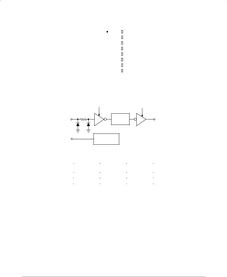
LOGIC DIAGRAM
|
VCC |
|
VDD |
INPUT |
|
LEVEL |
OUTPUT |
|
SHIFTER |
||
|
|
|
|
MODE |
TTL/CMOS |
|
|
MODE SELECT |
|
|
|
|
|
|
|
Input Logic |
Output Logic |
Mode Select |
Levels |
Levels |
|
|
|
1 (VCC) |
TTL |
CMOS |
0 (VSS) |
CMOS |
CMOS |
1/6 of package shown.
http://onsemi.com
2

MC14504B
ELECTRICAL CHARACTERISTICS (Voltages Referenced to VSS)
|
|
|
VCC |
VDD |
± 55_C |
|
25_C |
|
125_C |
|
|||
|
|
|
|
|
|
|
|
|
|
|
|||
Characteristic |
|
Symbol |
Vdc |
Vdc |
Min |
Max |
Min |
Typ (4.) |
Max |
Min |
Max |
Unit |
|
Output Voltage |
ª0º Level |
VOL |
Ð |
5.0 |
Ð |
0.05 |
Ð |
0 |
0.05 |
Ð |
0.05 |
Vdc |
|
Vin = 0 V |
|
|
Ð |
10 |
Ð |
0.05 |
Ð |
0 |
0.05 |
Ð |
0.05 |
|
|
|
|
|
Ð |
1 5 |
Ð |
0.05 |
Ð |
0 |
0.05 |
Ð |
0.05 |
|
|
|
ªº1ºLevel |
|
|
|
|
|
|
|
|
|
|
|
|
Vin = VCC |
VOH |
Ð |
5.0 |
4.95 |
Ð |
4.95 |
5.0 |
Ð |
4.95 |
Ð |
Vdc |
||
|
|||||||||||||
|
|
|
Ð |
10 |
9.95 |
Ð |
9.95 |
10 |
Ð |
9.95 |
Ð |
|
|
|
|
|
Ð |
15 |
14.95 |
Ð |
14.95 |
15 |
Ð |
14.95 |
Ð |
|
|
|
|
|
|
|
|
|
|
|
|
|
|
|
|
Input Voltage |
ª0º Level |
VIL |
|
|
|
|
|
|
|
|
|
Vdc |
|
(VOL = 1.0 Vdc) TTL±CMOS |
|
|
5.0 |
10 |
Ð |
0.8 |
Ð |
1.3 |
0.8 |
Ð |
0.8 |
|
|
(VOL = 1.5 Vdc) TTL±CMOS |
|
|
5.0 |
15 |
Ð |
0.8 |
Ð |
1.3 |
0.8 |
Ð |
0.8 |
|
|
(VOL = 1.0 Vdc) CMOS±CMOS |
|
5.0 |
10 |
Ð |
1.5 |
Ð |
2.25 |
1.5 |
Ð |
1.4 |
|
||
(VOL = 1.5 Vdc) CMOS±CMOS |
|
5.0 |
15 |
Ð |
1.5 |
Ð |
2.25 |
1.5 |
Ð |
1.5 |
|
||
(VOL = 1.5 Vdc) CMOS±CMOS |
|
10 |
15 |
Ð |
3.0 |
Ð |
4.5 |
3.0 |
Ð |
2.9 |
|
||
Input Voltage |
ª1º Level |
VIH |
|
|
|
|
|
|
|
|
|
Vdc |
|
(VOH = 9.0 Vdc) TTL±CMOS |
|
|
5.0 |
10 |
2.0 |
Ð |
2.0 |
1.5 |
Ð |
2.0 |
Ð |
|
|
(VOH = 13.5 Vdc) TTL±CMOS |
|
5.0 |
15 |
2.0 |
Ð |
2.0 |
1.5 |
Ð |
2.0 |
Ð |
|
||
(VOH = 9.0 Vdc) CMOS±CMOS |
|
5.0 |
10 |
3.6 |
Ð |
3.5 |
2.75 |
Ð |
3.5 |
Ð |
|
||
(VOH = 13.5 Vdc) CMOS±CMOS |
|
5.0 |
15 |
3.6 |
Ð |
3.5 |
2.75 |
Ð |
3.5 |
Ð |
|
||
(VOH = 13.5 Vdc) CMOS±CMOS |
|
10 |
15 |
7.1 |
Ð |
7.0 |
5.5 |
Ð |
7.0 |
Ð |
|
||
Output Drive Current |
|
IOH |
|
|
|
|
|
|
|
|
|
mAdc |
|
(VOH = 2.5 Vdc) |
Source |
|
Ð |
5.0 |
± 3.0 |
Ð |
± 2.4 |
± 4.2 |
Ð |
± 1.7 |
Ð |
|
|
(VOH = 4.6 Vdc) |
|
|
Ð |
5.0 |
± 0.64 |
Ð |
± 0.51 |
± 0.88 |
Ð |
± 0.36 |
Ð |
|
|
(VOH = 9.5 Vdc) |
|
|
Ð |
10 |
± 1.6 |
Ð |
± 1.3 |
± 2.25 |
Ð |
± 0.9 |
Ð |
|
|
(VOH = 13.5 Vdc) |
|
|
Ð |
15 |
± 4.2 |
Ð |
± 3.4 |
± 8.8 |
Ð |
± 2.4 |
Ð |
|
|
(VOL = 0.4 Vdc) |
Sink |
I |
Ð |
5.0 |
0.64 |
Ð |
0.51 |
0.88 |
Ð |
0.36 |
Ð |
mAdc |
|
(VOL = 0.5 Vdc) |
|
OL |
Ð |
10 |
1.6 |
Ð |
1.3 |
2.25 |
Ð |
0.9 |
Ð |
|
|
|
|
|
|||||||||||
(VOL = 1.5 Vdc) |
|
|
Ð |
15 |
4.2 |
Ð |
3.4 |
8.8 |
Ð |
2.4 |
Ð |
|
|
Input Current |
|
Iin |
Ð |
15 |
Ð |
± 0.1 |
Ð |
± 0.00001 |
± 0.1 |
Ð |
± 1.0 |
μAdc |
|
Input Capacitance (Vin = 0) |
|
Cin |
Ð |
Ð |
Ð |
Ð |
Ð |
5.0 |
7.5 |
Ð |
Ð |
pF |
|
Quiescent Current |
|
IDD or |
Ð |
5.0 |
Ð |
0.05 |
Ð |
0.0005 |
0.05 |
Ð |
1.5 |
μAdc |
|
(Per Package) |
|
ICC |
Ð |
10 |
Ð |
0.10 |
Ð |
0.0010 |
0.10 |
Ð |
3.0 |
|
|
CMOS±CMOS Mode |
|
|
Ð |
15 |
Ð |
0.20 |
Ð |
0.0015 |
0.20 |
Ð |
6.0 |
|
|
|
|
|
|
|
|
|
|
|
|
|
|
|
|
Quiescent Current |
|
IDD |
5.0 |
5.0 |
Ð |
0.5 |
Ð |
0.0005 |
0.5 |
Ð |
3.8 |
μAdc |
|
(Per Package) |
|
|
5.0 |
10 |
Ð |
1.0 |
Ð |
0.0010 |
1.0 |
Ð |
7.5 |
|
|
TTL±CMOS Mode |
|
|
5.0 |
15 |
Ð |
2.0 |
Ð |
0.0015 |
2.0 |
Ð |
15 |
|
|
|
|
|
|
|
|
|
|
|
|
|
|
|
|
Quiescent Current |
|
ICC |
5.0 |
5.0 |
Ð |
5.0 |
Ð |
2.5 |
5.0 |
Ð |
6.0 |
mAdc |
|
(Per Package) |
|
|
5.0 |
10 |
Ð |
5.0 |
Ð |
2.5 |
5.0 |
Ð |
6.0 |
|
|
TTL±CMOS Mode |
|
|
5.0 |
15 |
Ð |
5.0 |
Ð |
2.5 |
5.0 |
Ð |
6.0 |
|
|
|
|
|
|
|
|
|
|
|
|
|
|
|
|
4. Data labelled ªTypº is not to be used for design purposes but is intended as an indication of the IC's potential performance.
http://onsemi.com
3
 Loading...