


MOTOROLA
SEMICONDUCTOR TECHNICAL DATA
Voltage |
Controlled |
Oscillator |
|
MC1648 |
Consider |
MC12148 for |
|
|
|
New Designs |
|
|||
The MC1648 requires an external parallel tank circuit consisting of the |
VOLTAGE |
|||
inductor (L) and capacitor (C). For Maximum Performance QL ≥ 100 at |
||||
Frequency of Operation. |
|
|
CONTROLLED |
|
|
|
|
|
|
A varactor diode may be incorporated into the tank circuit to provide a
voltage variable input for the oscillator (VCO). The MC1648 was OSCILLATOR designed for use in the Motorola Phase±Locked Loop shown in Figure 9.
This device may also be used in many other applications requiring a fixed or variable frequency clock source of high spectral purity. (See Figure 2)
The MC1648 may be operated from a +5.0Vdc supply or a ±5.2Vdc supply, depending upon system requirements.
NOTE: The MC1648 is NOT useable as a crystal oscillator.
Pinout: 14±Lead Package (Top View) |
|
|
L SUFFIX |
||||||||||||||
|
|
|
|
|
|
|
|
|
|
|
|
|
|
|
|
|
|
VCC |
NC |
TANK |
NC |
BIAS |
NC |
|
VEE |
14±LEAD CERAMIC PACKAGE |
|||||||||
|
|
CASE 632±08 |
|||||||||||||||
|
14 |
|
13 |
|
12 |
|
11 |
|
10 |
|
9 |
|
8 |
|
|
||
|
|
|
|
|
|
|
|
Not Recommended for New Designs |
|||||||||
|
|
|
|
|
|
|
|
|
|
|
|
|
|
|
|||
|
|
|
|
|
|
|
|
|
|
|
|
|
|
|
|
|
|
|
|
|
|
|
|
|
|
|
|
|
|
|
|
|
|
|
|
|
|
|
|
|
|
|
|
|
|
|
|
|
|
|
|
|
|
|
|
|
|
|
|
|
|
|
|
|
|
|
|
|
|
|
|
|
|
|
|
|
|
|
|
|
|
|
|
|
|
|
|
|
|
|
|
|
|
|
|
|
|
|
|
|
|
|
|
|
|
|
|
|
1 |
2 |
3 |
4 |
5 |
6 |
7 |
|
|
|
|
|
VCC NC |
OUT |
NC |
AGC |
NC |
VEE |
|
|
P SUFFIX |
||
|
|
|
|
|
|
|
|
|
|
14±LEAD PLASTIC PACKAGE |
|
|
Pin assignment is for Dual±in±Line Package. |
|
|
CASE 646±06 |
|||||||
|
|
|
|
||||||||
For PLCC pin assignment, see the MC1648 Non±Standard Pin Conversion Table below. |
|
||||||||||
MC1648 NON±STANDARD PIN CONVERSION DATA |
|
|
D SUFFIX |
||||||||
|
|
8±PIN PLASTIC SOIC PACKAGE |
|||||||||
Package |
TANK |
VCC |
VCC |
OUT |
AGC |
VEE |
VEE |
BIAS |
|||
CASE 751±05 |
|||||||||||
8 D |
1 |
2 |
3 |
4 |
|
5 |
6 |
7 |
8 |
|
|
14 L,P |
12 |
14 |
1 |
3 |
|
5 |
7 |
8 |
10 |
|
|
20FN |
18 |
20 |
2 |
4 |
|
8 |
10 |
12 |
14 |
|
|
*NOTE ± All unused pins are not connected. |
|
|
|
|
|
FN SUFFIX |
|||||
|
|
|
|
|
|
|
|
|
|
||
Supply Voltage |
|
GND Pins |
|
Supply Pins |
|
20±LEAD PLCC PACKAGE |
|||||
|
|
|
CASE 775±02 |
||||||||
+5.0Vdc |
|
|
7,8 |
|
|
|
1,14 |
|
|
||
±5.2Vdc |
|
|
1,14 |
|
|
|
7,8 |
|
|
||
LOGIC DIAGRAM
BIAS POINT 10 |
3 |
TANK 12 |
OUTPUT |
|
|
|
5 |
|
AGC |
•Input Capacitance = 6.0pF (TYP)
•Maximum Series Resistance for L (External Inductance) = 50Ω (TYP)
•Power Dissipation = 150mW (TYP)/Pkg (+5.0Vdc Supply)
•Maximum Output Frequency = 225MHz (TYP)
VCC1 = Pin 1
VCC2 = Pin 14
VEE = Pin 7
1/97
Motorola, Inc. 1997 |
1 |
REV 2 |
MC1648 |
|
|
|
|
|
|
|
|
|
|
VCC2 |
|
VCC1 |
|
|
|
|
14 |
|
1 |
|
|
|
Q9 |
|
|
Q1 |
|
|
|
|
|
Q3 |
Q2 |
|
|
|
|
|
|
3 |
|
|
|
|
|
|
OUTPUT |
|
|
|
|
|
Q4 |
|
Q11 |
Q10 |
|
Q7 |
Q6 |
|
|
|
|
|
|
|
D1 |
|
|
|
|
|
|
Q5 |
|
|
|
D2 |
Q8 |
|
|
|
|
|
|
|
|
|
|
|
7 |
10 |
12 |
8 |
5 |
|
|
VEE1 |
BIAS |
TANK |
VEE |
AGC |
|
|
|
POINT |
|
|
|
|
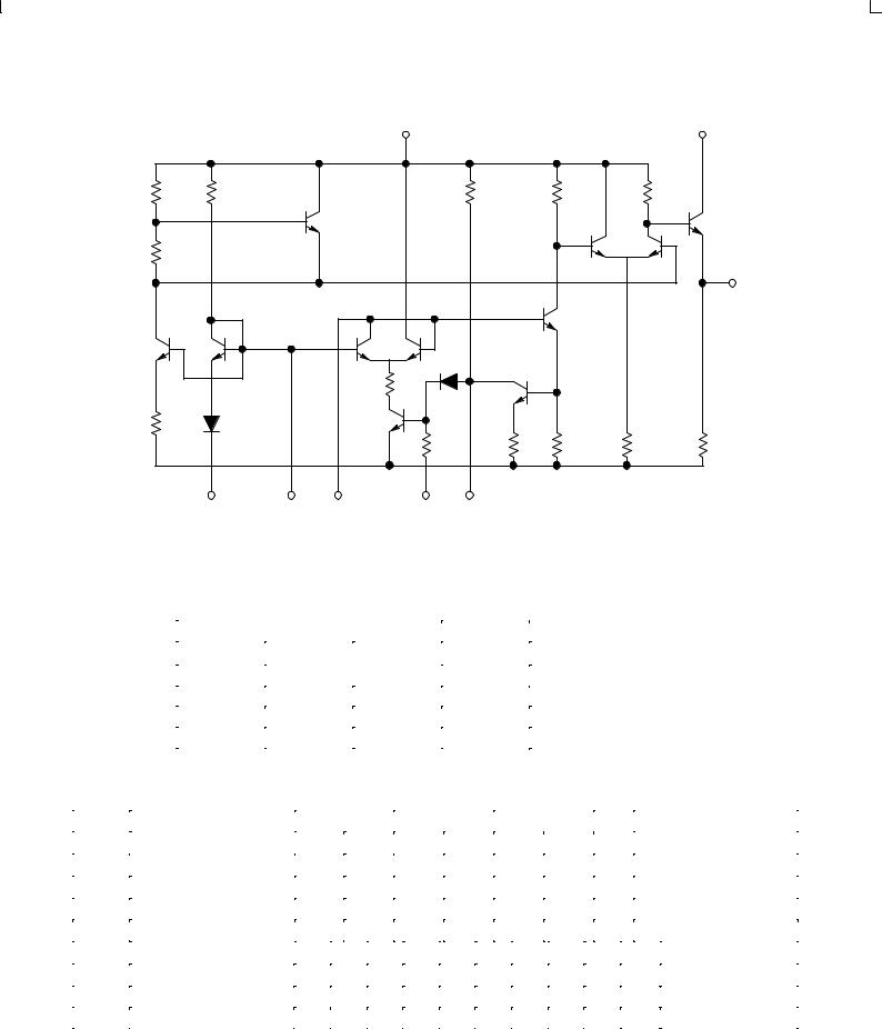
Figure 1. Circuit Schematic
TEST VOLTAGE/CURRENT VALUES
@ Test |
|
(Volts) |
|
mAdc |
|
Temperature |
|
|
|
|
|
VIHmax |
VILmin |
VCC |
IL |
||
|
|||||
|
MC1648 |
|
|
|
|
|
|
|
|
|
|
±30°C |
+2.0 |
+1.5 |
+5.0 |
±5.0 |
|
+25°C |
|
|
|
|
|
+1.85 |
+1.35 |
+5.0 |
±5.0 |
||
+85°C |
|
|
|
|
|
+1.7 |
+1.2 |
+5.0 |
±5.0 |
||
|
|
|
|
|
Note: SOIC ªDº package guaranteed ±30°C to +70°C only
ELECTRICAL CHARACTERISTICS (Supply Voltage = +5.0V)
|
|
|
±30°C |
|
|
|
+25°C |
|
|
|
+85°C |
|
|
|
|
|
|
|
|||||||||
|
|
|
|
|
|
|
|
|
|
|
|
|
|
|
|
|
|
|
|
|
|
|
|
|
|
|
|
|
Symbol |
Characteristic |
Min |
|
Max |
|
Min |
|
|
Max |
|
|
Min |
|
Max |
|
Unit |
|
|
Condition |
|
||||||
|
|
|
|
|
|
|
|
|
|
|
|
|
|
|
|
|
|
|
|
|
|
|
|
|
|
|
|
|
IE |
Power Supply Drain Current |
± |
|
|
|
± |
|
± |
|
|
41 |
|
|
|
± |
|
± |
|
mAdc |
|
Inputs and outputs open |
|
||||
|
VOH |
Logic ª1º Output Voltage |
3.955 |
|
4.185 |
|
4.04 |
|
|
4.25 |
|
|
4.11 |
|
4.36 |
|
Vdc |
|
VILmin to Pin 12, IL @ Pin 3 |
|
|||||||
|
VOL |
Logic ª0º Output Voltage |
3.16 |
|
|
|
3.4 |
|
3.2 |
|
|
3.43 |
|
|
3.22 |
|
3.475 |
|
Vdc |
|
VIHmax to Pin 12, IL @ Pin 3 |
|
|||||
|
VBIAS1 |
Bias Voltage |
1.6 |
|
|
|
1.9 |
|
1.45 |
|
|
1.75 |
|
|
1.3 |
|
1.6 |
|
Vdc |
|
VILmin to Pin 12 |
|
|||||
|
|
|
Min |
|
Typ |
|
Max |
Min |
|
|
Typ |
|
Max |
|
Min |
Typ |
Max |
|
Unit |
Condition |
|
||||||
|
|
|
|
|
|
|
|
|
|
|
|
|
|
|
|
|
|
|
|
|
|
|
|||||
|
VP±P |
Peak±to±Peak Tank Voltage |
± |
|
± |
|
± |
|
± |
|
400 |
|
± |
|
± |
|
± |
± |
|
mV |
See Figure 3 |
|
|||||
|
Vdc |
Output Duty Cycle |
± |
|
± |
|
± |
|
± |
|
50 |
|
± |
|
± |
|
± |
± |
|
% |
|
|
|||||
|
|
|
|
|
|
|
|
|
|
|
|
|
|
|
|
|
|
|
|
|
|
|
|||||
|
fmax2 |
Oscillation Frequency |
± |
|
225 |
|
± |
|
200 |
|
225 |
|
± |
|
± |
|
225 |
± |
|
MHz |
|
|
|||||
|
1. This measurement guarantees the dc potential at the bias point for purposes of incorporating a varactor tuning diode at this point. |
||||||||||||||||||||||||||
|
2. Frequency variation over temperature is a direct function of the C/ |
|
Temperature and L/ |
Temperature. |
|
|
|
|
|||||||||||||||||||
|
|
|
|
|
|
|
|
|
|
|
|
|
|
|
|
|
|
|
|
|
|
|
|
|
|
|
|
|
MOTOROLA |
|
|
|
|
|
|
|
|
2 |
|
|
|
|
|
|
|
|
|
|
|
|
|
|
HIPERCOMM |
||
|
|
|
|
|
|
|
|
|
|
|
|
|
|
|
|
|
|
|
|
|
|
|
|
|
|
BR1334 Ð Rev 4 |
|
|
|
|
|
MC1648 |
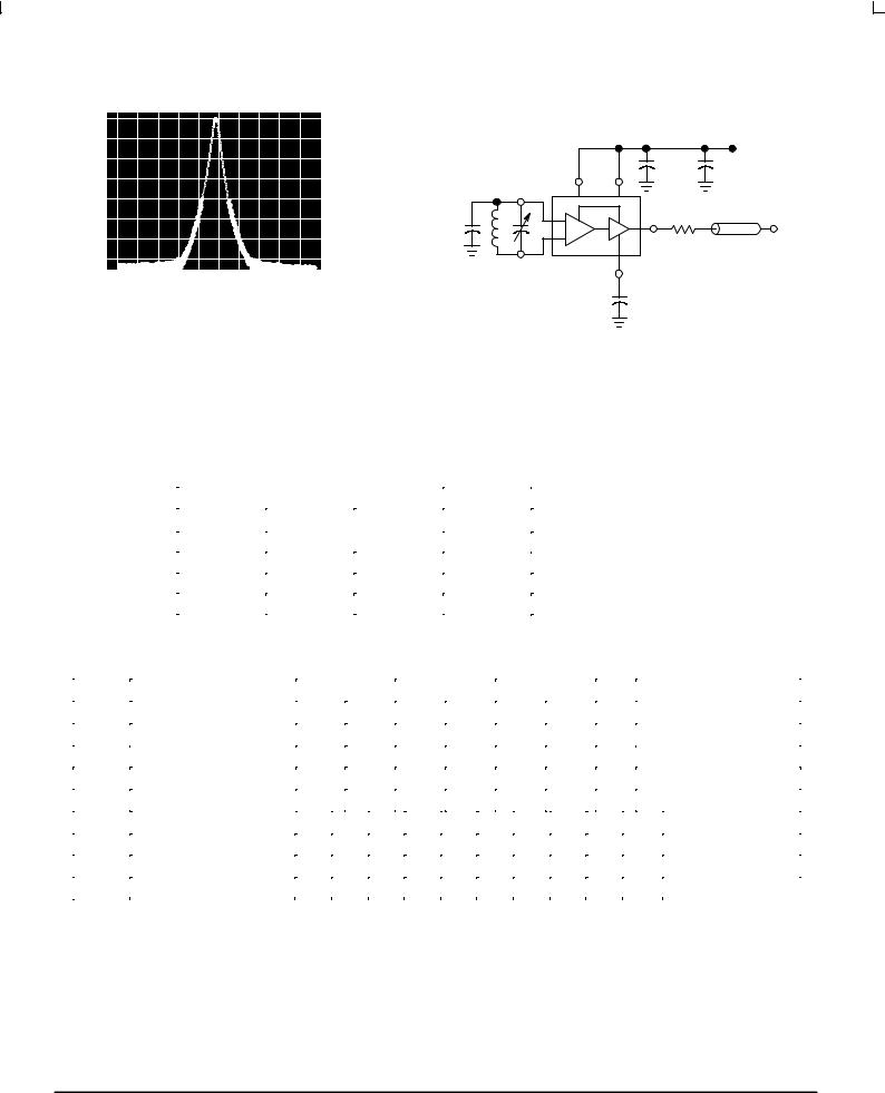
L: Micro Metal torroid #T20±22, 8 turns #30 Enameled Copper wire. |
L=40nH |
|||
C = 3.0±35pF |
|
|
|
C=10pF |
|
|
|
|
+5.0Vdc |
|
|
|
0.1μF |
10μF |
|
|
14 |
1 |
|
|
|
10 |
|
|
|
|
|
1200* |
|
0.1μF |
L |
C |
3 |
|
|
|
|
SIGNAL |
|
|
|
|
|
|
|
|
12 |
|
UNDER |
|
|
5 |
TEST |
|
B.W. = 10 kHz |
|
|
||
|
|
0.1μF |
|
|
Center Frequency = 100 MHz |
|
|
|
|
Scan Width = 50 kHz/div |
|
|
|
|
Vertical Scale = 10 dB/div |
|
|
|
|
*The 1200 ohm resistor and the scope termination impedance constitute a 25:1 attenuator probe. Coax shall be CT±075±50 or equivalent.
Figure 2. Spectral Purity of Signal Output for 200MHz Testing
TEST VOLTAGE/CURRENT VALUES
@ Test |
|
(Volts) |
|
mAdc |
|
Temperature |
|
|
|
|
|
VIHmax |
VILmin |
VEE |
IL |
||
|
|||||
|
MC1648 |
|
|
|
|
|
|
|
|
|
|
±30°C |
±3.2 |
±3.7 |
±5.2 |
±5.0 |
|
+25°C |
|
|
|
|
|
±3.35 |
±3.85 |
±5.2 |
±5.0 |
||
+85°C |
|
|
|
|
|
±3.5 |
±4.0 |
±5.2 |
±5.0 |
||
|
|
|
|
|
Note: SOIC ªDº package guaranteed ±30°C to +70°C only
ELECTRICAL CHARACTERISTICS (Supply Voltage = ±5.2V)
|
|
±30°C |
|
|
|
+25°C |
|
|
|
+85°C |
|
|
|
|
|
|
|||||||||
|
|
|
|
|
|
|
|
|
|
|
|
|
|
|
|
|
|
|
|
|
|
|
|
|
|
Symbol |
Characteristic |
Min |
|
Max |
|
Min |
|
Max |
|
|
Min |
|
Max |
|
Unit |
|
|
Condition |
|||||||
|
|
|
|
|
|
|
|
|
|
|
|
|
|
|
|
|
|
|
|
|
|
|
|
|
|
IE |
Power Supply Drain Current |
± |
|
|
|
± |
|
± |
|
41 |
|
|
|
± |
|
± |
|
|
mAdc |
|
Inputs and outputs open |
||||
VOH |
Logic ª1º Output Voltage |
±1.045 |
|
±0.815 |
|
±0.96 |
|
±0.75 |
|
±0.89 |
|
±0.64 |
|
|
Vdc |
|
VILmin to Pin 12, IL @ Pin 3 |
||||||||
VOL |
Logic ª0º Output Voltage |
±1.89 |
|
±1.65 |
|
±1.85 |
|
±1.62 |
|
±1.83 |
|
±1.575 |
|
Vdc |
|
VIHmax to Pin 12, IL @ Pin 3 |
|||||||||
VBIAS1 |
Bias Voltage |
±3.6 |
|
|
±3.3 |
|
±3.75 |
|
±3.45 |
|
±3.9 |
|
±3.6 |
|
|
Vdc |
|
VILmin to Pin 12 |
|||||||
|
|
Min |
|
Typ |
|
Max |
Min |
|
Typ |
|
Max |
Min |
Typ |
|
Max |
|
Unit |
Condition |
|||||||
|
|
|
|
|
|
|
|
|
|
|
|
|
|
|
|
|
|
|
|
|
|||||
VP±P |
Peak±to±Peak Tank Voltage |
± |
|
± |
|
± |
|
± |
400 |
|
± |
|
± |
|
± |
|
± |
|
mV |
See Figure 3 |
|||||
Vdc |
Output Duty Cycle |
± |
|
± |
|
± |
|
± |
50 |
|
± |
|
± |
|
± |
|
± |
|
% |
|
|||||
|
|
|
|
|
|
|
|
|
|
|
|
|
|
|
|
|
|
|
|
|
|||||
fmax2 |
Oscillation Frequency |
± |
|
225 |
|
± |
|
200 |
225 |
|
± |
|
± |
|
225 |
|
± |
|
MHz |
|
|||||
1. This measurement guarantees the dc potential at the bias point for purposes of incorporating a varactor tuning diode at this point. |
|||||||||||||||||||||||||
2. Frequency variation over temperature is a direct function of the C/ |
Temperature and L/ |
Temperature. |
|
|
|
||||||||||||||||||||
HIPERCOMM |
3 |
MOTOROLA |
BR1334 Ð Rev 4 |
|
|

MC1648
|
|
|
VCC |
|
|
|
|
|
|
*** |
** |
|
10 |
1 |
14 |
|
|
|
|
|
|||
|
|
|
|
3 |
1200 |
0.1μF |
L |
C |
|
|
|
|
|
|
|||
|
12 |
7 |
8 |
5 |
0.1μF |
|
|
||||
|
|
|
|
|
|
|
0.1μF |
*** |
0.1μF |
QL ≥ 100 |
|
|
* |
|
VEE |
|
|
|
|
|
|
||
*Use high impedance probe (>1.0 Megohm must be used).
**The 1200 ohm resistor and the scope termination impedance constitute a 25:1 attenuator probe. Coax shall be CT±070±50 or equivalent.
***Bypass only that supply opposite ground.
VP±P |
50% |
ta |
PRF = 1.0MHz |
ta |
|
|
tb |
Duty Cycle (Vdc) ± |
|
||
tb |
||||
|
|
|||
Figure 3. Test Circuit and Waveforms
OPERATING CHARACTERISTICS
Figure 1 illustrates the circuit schematic for the MC1648. The oscillator incorporates positive feedback by coupling the base of transistor Q6 to the collector of Q7. An automatic gain control (AGC) is incorporated to limit the current through the emitter±coupled pair of transistors (Q7 and Q6) and allow optimum frequency response of the oscillator.
VEE (≈1.4V for positive supply operation).
When the MC1648 is used with a constant dc voltage to the varactor diode, the output frequency will vary slightly because of internal noise. This variation is plotted versus operating frequency in Figure 5.
In order to maintain the high Q of the oscillator, and provide high spectral purity at the output, transistor Q4 is used to translate the oscillator signal to the output differential pair Q2 and Q3. Q2 and Q3, in conjunction with output transistor Q1, provides a highly buffered output which produces a square wave. Transistors Q9 and Q11 provide the bias drive for the oscillator and output buffer. Figure 2 indicates the high spectral purity of the oscillator output (pin 3).
When operating the oscillator in the voltage controlled mode (Figure 4), it should be noted that the cathode of the
varactor diode (D) should be biased at least ª2º V above BE
|
10 |
|
||
0.1μF |
L |
|
3 |
|
D |
|
Output |
||
|
|
|
||
Vin |
12 |
|
||
C1 |
5 |
|||
|
|
|||
|
QL ≥ |
100 |
C2 |
|
|
|
|||
Figure 4. The MC1648 Operating in the
Voltage Controlled Mode
(Hz) |
100 |
|
|
|
|
|
|
DEVIATION, RMS |
|
VCC = 5 Vdc |
|
10 |
|
|
|
f, FREQUENCY |
|
|
|
|
|
|
|
|
1 |
|
|
|
1 |
10 |
100 |
|
|
f, OPERATING FREQUENCY (MHz) |
|
Oscillator Tank Components
(Circuit of Figure 4)
f |
|
L |
MHz |
D |
μH |
|
|
|
1.0±10 |
MV2115 |
100 |
10±60 |
MV2115 |
2.3 |
60±100 |
MV2106 |
0.15 |
|
|
|
|
|
|
|
|
|
|
|
|
|
|
|
Signal Generator |
|
|
|
|
|
|
20kHz above MC1648 Frequency |
|
|
|
|
300mV |
|
HP608 or Equiv |
|
|
|
|
|||
|
|
|
|
|
|
|
|
|
|
|
||||||
|
|
|
|
10mV |
|
|
|
|
|
20kHz |
|
|
|
|
|
|
|
|
|
|
|
|
|
|
|
|
|
|
|
||||
MC1648 |
|
|
Attenuator |
Product |
|
BW=1.0kHz Frequency |
|
Voltmeter RMS |
||||||||
|
|
|
|
|
|
|
|
|
|
|
|
|
|
|
|
|
Under Test |
|
|
MC1648 |
|
Detector |
|
|
Meter HP5210A or Equiv |
|
HP3400A or Equiv |
||||||
|
|
|
|
|
||||||||||||
|
|
|
|
|
|
|
|
|
|
|
|
|
|
|||
|
|
|
|
Frequency (f) |
|
|
|
|
|
|
|
|
|
|
||
Frequency Deviation + (HP5210A output voltage) (Full Scale Frequency) 1.0Volt
Figure 5. Noise Deviation Test Circuit and Waveform
MOTOROLA |
4 |
HIPERCOMM |
|
|
BR1334 Ð Rev 4 |
 Loading...