


MOTOROLA MC14511BDWR2, MC14511BF, MC14511BFEL, MC14511BFR1, MC14511BCP Datasheet
...
MC14511B
BCD-To-Seven Segment
Latch/Decoder/Driver
The MC14511B BCD±to±seven segment latch/decoder/driver is constructed with complementary MOS (CMOS) enhancement mode devices and NPN bipolar output drivers in a single monolithic structure. The circuit provides the functions of a 4±bit storage latch, an 8421 BCD±to±seven segment decoder, and an output drive capability. Lamp test (LT), blanking (BI), and latch enable (LE) inputs are used to test the display, to turn±off or pulse modulate the brightness of the display, and to store a BCD code, respectively. It can be used with seven±segment light±emitting diodes (LED), incandescent, fluorescent, gas discharge, or liquid crystal readouts either directly or indirectly.
Applications include instrument (e.g., counter, DVM, etc.) display driver, computer/calculator display driver, cockpit display driver, and various clock, watch, and timer uses.
•Low Logic Circuit Power Dissipation
•High±Current Sourcing Outputs (Up to 25 mA)
•Latch Storage of Code
•Blanking Input
•Lamp Test Provision
•Readout Blanking on all Illegal Input Combinations
•Lamp Intensity Modulation Capability
•Time Share (Multiplexing) Facility
•Supply Voltage Range = 3.0 V to 18 V
•Capable of Driving Two Low±power TTL Loads, One Low±power Schottky TTL Load or Two HTL Loads Over the Rated Temperature Range
•Chip Complexity: 216 FETs or 54 Equivalent Gates
•Triple Diode Protection on all Inputs
MAXIMUM RATINGS (Voltages Referenced to V ) (2.) |
|
||
|
|
SS |
|
Symbol |
Parameter |
Value |
Unit |
|
|
|
|
VDD |
DC Supply Voltage Range |
± 0.5 to +18.0 |
V |
Vin |
Input Voltage Range, All Inputs |
± 0.5 to VDD + 0.5 |
V |
I |
DC Current Drain per Input Pin |
10 |
mA |
|
|
|
|
PD |
Power Dissipation, |
500 |
mW |
|
per Package (3.) |
|
|
TA |
Operating Temperature Range |
± 55 to +125 |
°C |
Tstg |
Storage Temperature Range |
± 65 to +150 |
°C |
IOHmax |
Maximum Output Drive Current |
25 |
mA |
|
(Source) per Output |
|
|
|
|
|
|
POHmax |
Maximum Continuous Output |
50 |
mA |
|
Power (Source) per Output (4.) |
|
|
2.Maximum Ratings are those values beyond which damage to the device may occur.
3.Temperature Derating:
Plastic ªP and D/DWº Packages: ± 7.0 mW/C From 65_C To 125_C
4.POHmax = IOH (VDD ± VOH)
http://onsemi.com
|
|
MARKING |
|
|
DIAGRAMS |
|
|
16 |
|
PDIP±16 |
MC14511BCP |
|
P SUFFIX |
|
|
AWLYYWW |
|
|
CASE 648 |
|
|
|
|
|
|
1 |
|
|
16 |
|
SOIC±16 |
14511B |
|
D SUFFIX |
|
|
AWLYWW |
|
|
CASE 751B |
|
|
|
|
|
|
1 |
|
|
16 |
|
SOIC±16 |
14511B |
|
|
|
|
DW SUFFIX |
|
|
CASE 751G |
AWLYYWW |
|
|
|
|
|
1 |
|
|
16 |
|
SOEIAJ±16 |
MC14511B |
|
F SUFFIX |
|
|
AWLYWW |
|
|
CASE 966 |
|
|
|
|
|
|
1 |
A |
= Assembly Location |
|
WL or L = Wafer Lot |
|
|
YY or Y |
= Year |
|
WW or W = Work Week |
||
ORDERING INFORMATION |
||
Device |
Package |
Shipping |
MC14511BCP |
PDIP±16 |
2000/Box |
MC14511BD |
SOIC±16 |
48/Rail |
MC14511BDW |
SOIC±16 |
47/Rail |
MC14511BDWR2 |
SOIC±16 |
1000/Tape & Reel |
MC14511BF |
SOEIAJ±16 |
See Note 1. |
MC14511BFEL |
SOEIAJ±16 |
See Note 1. |
1.For ordering information on the EIAJ version of the SOIC packages, please contact your local ON Semiconductor representative.
Semiconductor Components Industries, LLC, 2000 |
1 |
Publication Order Number: |
March, 2000 ± Rev. 3 |
|
MC14511B/D |
MC14511B
This device contains protection circuitry to protect the inputs against damage due to high static voltages or electric fields. However, it is advised that normal precautions be taken to avoid application of any voltage higher than maximum rated voltages to this high±impedance circuit. A
destructive high current mode may occur if Vin and Vout are not constrained to the range VSS v (Vin or Vout) v VDD.
Due to the sourcing capability of this circuit, damage can occur to the device if VDD is applied, and the outputs are shorted to VSS and are at a logical 1 (See Maximum Ratings).
Unused inputs must always be tied to an appropriate logic voltage level (e.g., either VSS or VDD).
PIN ASSIGNMENT
|
|
|
|
B |
|
1 |
|
16 |
|
|
VDD |
|
|
|
|||
|
|
|
|
|
|
|
|
|
|
|
|||||||
|
|
|
|
|
|
|
|
|
|
|
|||||||
|
|
|
|
C |
|
2 |
|
15 |
|
|
f |
|
a |
||||
|
|
|
|
|
|
|
|
|
|
|
|
|
g |
|
|||
|
|
LT |
|
3 |
|
14 |
|
|
f |
g b |
|||||||
|
|
|
|
|
|
|
|
|
|
|
|
|
|
|
|||
|
|
|
|
BI |
|
4 |
|
13 |
|
|
a |
e |
c |
||||
|
|
LE |
|
5 |
|
12 |
|
|
b |
||||||||
|
|
|
|
|
|
|
d |
||||||||||
|
|
|
|
D |
|
6 |
|
11 |
|
|
c |
|
|||||
|
|
|
|
|
|
|
|
|
|
|
|||||||
|
|
|
|
A |
|
7 |
|
10 |
|
|
d |
|
|
|
|||
|
|
|
|
|
|
|
|
|
|
|
|||||||
|
|
VSS |
|
8 |
|
9 |
|
|
e |
|
|
|
|||||
|
|
|
|
|
|
|
|
|
|||||||||
|
|
|
|
|
|
|
|
|
|||||||||
|
|
|
|
|
|
|
DISPLAY |
|
|
|
|
|
|
|
|||
|
|
|
|
|
|
|
|
|
|
|
|
|
|
|
|||
|
|
|
|
|
|
|
|
|
|
|
|
|
|
|
|
|
|
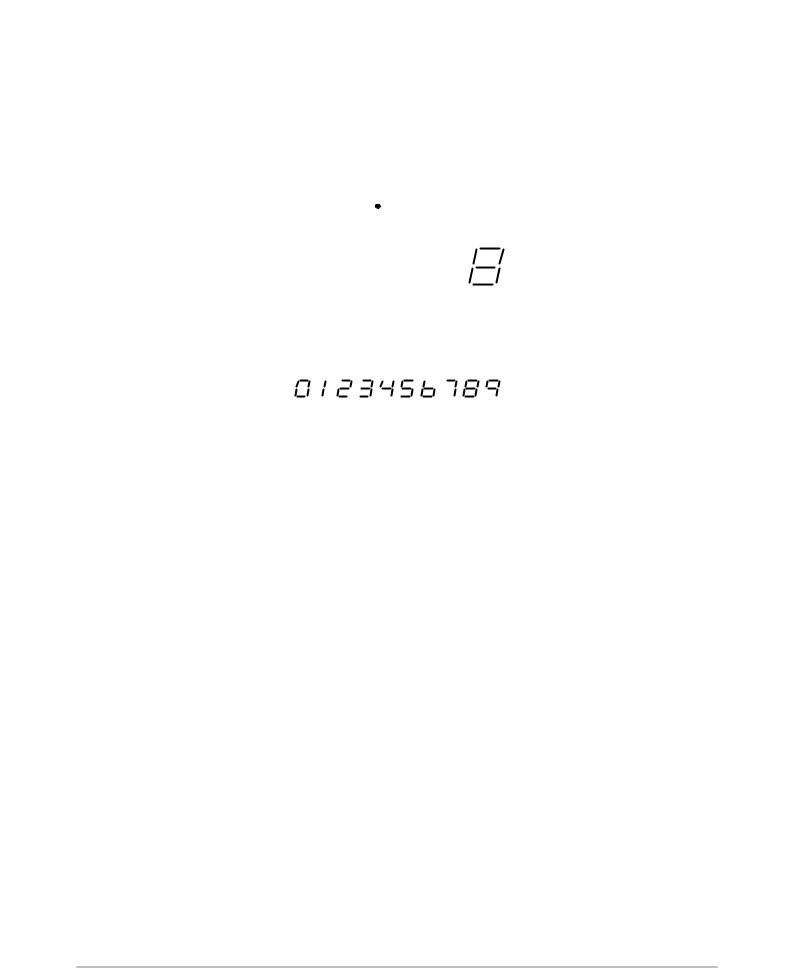
0 |
1 |
2 |
|
|
3 |
4 |
5 |
|
6 |
7 |
8 |
9 |
|
||||
TRUTH TABLE
|
|
|
Inputs |
|
|
|
|
|
|
Outputs |
|
|
||
LE |
BI |
LT |
D |
C |
B |
A |
a |
b |
c |
d |
e |
f |
g |
Display |
X |
X |
0 |
X X X X |
1 1 1 1 1 1 1 |
8 |
|||||||||
X |
0 |
1 |
X |
X |
X |
X |
0 |
0 |
0 |
0 |
0 |
0 |
0 |
Blank |
0 |
1 |
1 |
0 |
0 |
0 |
0 |
1 |
1 |
1 |
1 |
1 |
1 |
0 |
0 |
0 |
1 |
1 |
0 |
0 |
0 |
1 |
0 |
1 |
1 |
0 |
0 |
0 |
0 |
1 |
0 |
1 |
1 |
0 |
0 |
1 |
1 |
1 |
1 |
1 |
1 |
0 |
0 |
1 |
2 |
0 |
1 |
1 |
0 |
0 |
1 |
1 |
1 |
1 |
1 |
1 |
0 |
0 |
1 |
3 |
0 |
1 |
1 |
0 |
1 |
0 |
0 |
0 |
1 |
1 |
0 |
0 |
1 |
1 |
4 |
0 |
1 |
1 |
0 |
1 |
0 |
1 |
1 |
0 |
1 |
1 |
0 |
1 |
1 |
5 |
0 |
1 |
1 |
0 |
1 |
1 |
0 |
0 |
0 |
1 |
1 |
1 |
1 |
1 |
6 |
0 |
1 |
1 |
0 |
1 |
1 |
1 |
1 |
1 |
1 |
0 |
0 |
0 |
0 |
7 |
0 |
1 |
1 |
1 |
0 |
0 |
0 |
1 |
1 |
1 |
1 |
1 |
1 |
1 |
8 |
0 |
1 |
1 |
1 |
0 |
0 |
1 |
1 |
1 |
1 |
0 |
0 |
1 |
1 |
9 |
0 |
1 |
1 |
1 |
0 |
1 |
0 |
0 |
0 |
0 |
0 |
0 |
0 |
0 |
Blank |
0 |
1 |
1 |
1 |
0 |
1 |
1 |
0 |
0 |
0 |
0 |
0 |
0 |
0 |
Blank |
0 |
1 |
1 |
1 |
1 |
0 |
0 |
0 |
0 |
0 |
0 |
0 |
0 |
0 |
Blank |
0 |
1 |
1 |
1 |
1 |
0 |
1 |
0 |
0 |
0 |
0 |
0 |
0 |
0 |
Blank |
0 |
1 |
1 |
1 |
1 |
1 |
0 |
0 |
0 |
0 |
0 |
0 |
0 |
0 |
Blank |
0 |
1 |
1 |
1 |
1 |
1 |
1 |
0 |
0 |
0 |
0 |
0 |
0 |
0 |
Blank |
1 |
1 |
1 |
X |
X |
X |
X |
|
|
|
* |
|
|
|
* |
X = Don't Care
* Depends upon the BCD code previously applied when LE = 0
http://onsemi.com
2

MC14511B
ELECTRICAL CHARACTERISTICS (Voltages Referenced to VSS)
|
|
|
VDD |
± 55_C |
|
25_C |
|
|
125_C |
|
||
|
|
|
|
|
|
|
|
|
|
|
|
|
Characteristic |
|
Symbol |
Vdc |
Min |
Max |
Min |
Typ (5.) |
Max |
Min |
Max |
Unit |
|
Output Voltage |
ª0º Level |
VOL |
5.0 |
Ð |
0.05 |
Ð |
0 |
0.05 |
Ð |
0.05 |
Vdc |
|
Vin = VDD or 0 |
|
|
10 |
Ð |
0.05 |
Ð |
0 |
0.05 |
Ð |
0.05 |
|
|
|
|
|
15 |
Ð |
0.05 |
Ð |
0 |
0.05 |
Ð |
0.05 |
|
|
|
|
|
|
|
|
|
|
|
|
|
|
|
|
ª1º Level |
VOH |
5.0 |
4.1 |
Ð |
4.1 |
4.57 |
|
Ð |
4.1 |
Ð |
Vdc |
Vin = 0 or VDD |
|
|
10 |
9.1 |
Ð |
9.1 |
9.58 |
|
Ð |
9.1 |
Ð |
|
|
|
|
15 |
14.1 |
Ð |
14.1 |
14.59 |
|
Ð |
14.1 |
Ð |
|
|
|
|
|
|
|
|
|
|
|
|
|
|
Input Voltage # |
ª0º Level |
VIL |
|
|
|
|
|
|
|
|
|
Vdc |
(VO = 3.8 or 0.5 Vdc) |
|
|
5.0 |
Ð |
1.5 |
Ð |
2.25 |
|
1.5 |
Ð |
1.5 |
|
(VO = 8.8 or 1.0 Vdc) |
|
|
10 |
Ð |
3.0 |
Ð |
4.50 |
|
3.0 |
Ð |
3.0 |
|
(VO = 13.8 or 1.5 Vdc) |
|
|
15 |
Ð |
4.0 |
Ð |
6.75 |
|
4.0 |
Ð |
4.0 |
|
|
ª1º Level |
VIH |
5.0 |
3.5 |
Ð |
3.5 |
2.75 |
|
Ð |
3.5 |
Ð |
Vdc |
(VO = 0.5 or 3.8 Vdc) |
|
|
|
|
||||||||
(VO = 1.0 or 8.8 Vdc) |
|
|
10 |
7.0 |
Ð |
7.0 |
5.50 |
|
Ð |
7.0 |
Ð |
|
(VO = 1.5 or 13.8 Vdc) |
|
|
15 |
11 |
Ð |
11 |
8.25 |
|
Ð |
11 |
Ð |
|
Output Drive Voltage |
|
VOH |
|
|
|
|
|
|
|
|
|
Vdc |
(IOH = 0 mA) |
Source |
|
5.0 |
4.1 |
Ð |
4.1 |
4.57 |
|
Ð |
4.1 |
Ð |
|
(IOH = 5.0 mA) |
|
|
|
Ð |
Ð |
Ð |
4.24 |
|
Ð |
Ð |
Ð |
|
(IOH = 10 mA) |
|
|
|
3.9 |
Ð |
3.9 |
4.12 |
|
Ð |
3.5 |
Ð |
|
(IOH = 15 mA) |
|
|
|
Ð |
Ð |
Ð |
3.94 |
|
Ð |
Ð |
Ð |
|
(IOH = 20 mA) |
|
|
|
3.4 |
Ð |
3.4 |
3.70 |
|
Ð |
3.0 |
Ð |
|
(IOH = 25 mA) |
|
|
|
Ð |
Ð |
Ð |
3.54 |
|
Ð |
Ð |
Ð |
|
(IOH = 0 mA) |
|
|
10 |
9.1 |
Ð |
9.1 |
9.58 |
|
Ð |
9.1 |
Ð |
Vdc |
(IOH = 5.0 mA) |
|
|
|
Ð |
Ð |
Ð |
9.26 |
|
Ð |
Ð |
Ð |
|
(IOH = 10 mA) |
|
|
|
9.0 |
Ð |
9.0 |
9.17 |
|
Ð |
8.6 |
Ð |
|
(IOH = 15 mA) |
|
|
|
Ð |
Ð |
Ð |
9.04 |
|
Ð |
Ð |
Ð |
|
(IOH = 20 mA) |
|
|
|
8.6 |
Ð |
8.6 |
8.90 |
|
Ð |
8.2 |
Ð |
|
(IOH = 25 mA) |
|
|
|
Ð |
Ð |
Ð |
8.70 |
|
Ð |
Ð |
Ð |
|
(IOH = 0 mA) |
|
|
15 |
14.1 |
Ð |
14.1 |
14.59 |
|
Ð |
14.1 |
Ð |
Vdc |
(IOH = 5.0 mA) |
|
|
|
Ð |
Ð |
Ð |
14.27 |
|
Ð |
Ð |
Ð |
|
(IOH = 10 mA) |
|
|
|
14 |
Ð |
14 |
14.18 |
|
Ð |
13.6 |
Ð |
|
(IOH = 15 mA) |
|
|
|
Ð |
Ð |
Ð |
14.07 |
|
Ð |
Ð |
Ð |
|
(IOH = 20 mA) |
|
|
|
13.6 |
Ð |
13.6 |
13.95 |
|
Ð |
13.2 |
Ð |
|
(IOH = 25 mA) |
|
|
|
Ð |
Ð |
Ð |
13.70 |
|
Ð |
Ð |
Ð |
|
Output Drive Current |
|
IOL |
|
|
|
|
|
|
|
|
|
mAdc |
(VOL = 0.4 V) |
Sink |
|
5.0 |
0.64 |
Ð |
0.51 |
0.88 |
|
Ð |
0.36 |
Ð |
|
(VOL = 0.5 V) |
|
|
10 |
1.6 |
Ð |
1.3 |
2.25 |
|
Ð |
0.9 |
Ð |
|
(VOL = 1.5 V) |
|
|
15 |
4.2 |
Ð |
3.4 |
8.8 |
|
Ð |
2.4 |
Ð |
|
Input Current |
|
Iin |
15 |
Ð |
± 0.1 |
Ð |
± 0.00001 |
± 0.1 |
Ð |
± 1.0 |
μAdc |
|
Input Capacitance |
|
Cin |
Ð |
Ð |
Ð |
Ð |
5.0 |
|
7.5 |
Ð |
Ð |
pF |
Quiescent Current |
|
IDD |
5.0 |
Ð |
5.0 |
Ð |
0.005 |
|
5.0 |
Ð |
150 |
μAdc |
(Per Package) Vin = 0 or VDD, |
|
10 |
Ð |
10 |
Ð |
0.010 |
|
10 |
Ð |
300 |
|
|
Iout = 0 μA |
|
|
15 |
Ð |
20 |
Ð |
0.015 |
|
20 |
Ð |
600 |
|
Total Supply Current (6.) (7.) |
I |
5.0 |
|
|
I = (1.9 μA/kHz) f + I |
DD |
|
|
μAdc |
|||
|
|
T |
|
|
|
T |
|
|
|
|
|
|
(Dynamic plus Quiescent, |
|
10 |
|
|
IT = (3.8 μA/kHz) f + IDD |
|
|
|
||||
Per Package) |
|
|
15 |
|
|
IT = (5.7 μA/kHz) f + IDD |
|
|
|
|||
(CL = 50 pF on all outputs, all |
|
|
|
|
|
|
|
|
|
|
|
|
buffers switching) |
|
|
|
|
|
|
|
|
|
|
|
|
|
|
|
|
|
|
|
|
|
|
|
|
|
5.Noise immunity specified for worst±case input combination. Noise Margin for both ª1º and ª0º level =
1.0Vdc min @ VDD = 5.0 Vdc
2.0 Vdc min @ VDD = 10 Vdc
2.5Vdc min @ VDD = 15 Vdc
6.The formulas given are for the typical characteristics only at 25_C.
7.To calculate total supply current at loads other than 50 pF:
IT(CL) = IT(50 pF) + 3.5 x 10±3 (CL ± 50) VDDf
where: IT is in μA (per package), CL in pF, VDD in Vdc, and f in kHz is input frequency.
http://onsemi.com
3

MC14511B
SWITCHING CHARACTERISTICS (8.) (CL = 50 pF, TA = 25_C)
|
|
|
|
|
|
VDD |
|
|
|
|
|
|
|
|
Characteristic |
Symbol |
Vdc |
Min |
Typ |
Max |
Unit |
|
|
|
|
|
|
|
|
|
|
|
|
Output Rise Time |
tTLH |
|
|
|
|
ns |
|||
|
|
tTLH = (0.40 ns/pF) CL + 20 ns |
|
5.0 |
Ð |
40 |
80 |
|
||
|
|
tTLH = (0.25 ns/pF) CL + 17.5 ns |
|
10 |
Ð |
30 |
60 |
|
||
|
|
tTLH = (0.20 ns/pF) CL + 15 ns |
|
15 |
Ð |
25 |
50 |
|
||
|
Output Fall Time |
tTHL |
|
|
|
|
ns |
|||
|
|
tTHL = (1.5 ns/pF) CL + 50 ns |
|
5.0 |
Ð |
125 |
250 |
|
||
|
|
tTHL = (0.75 ns/pF) CL + 37.5 ns |
|
10 |
Ð |
75 |
150 |
|
||
|
|
tTHL = (0.55 ns/pF) CL + 37.5 ns |
|
15 |
Ð |
65 |
130 |
|
||
|
Data Propagation Delay Time |
tPLH |
|
|
|
|
ns |
|||
|
|
tPLH = (0.40 ns/pF) CL + 620 ns |
|
5.0 |
Ð |
640 |
1280 |
|
||
|
|
tPLH = (0.25 ns/pF) CL + 237.5 ns |
|
10 |
Ð |
250 |
500 |
|
||
|
|
tPLH = (0.20 ns/pF) CL + 165 ns |
|
15 |
Ð |
175 |
350 |
|
||
|
|
tPHL = (1.3 ns/pF) CL + 655 ns |
tPHL |
5.0 |
Ð |
720 |
1440 |
|
||
|
|
tPHL = (0.60 ns/pF) CL + 260 ns |
|
10 |
Ð |
290 |
580 |
|
||
|
|
tPHL = (0.35 ns/pF) CL + 182.5 ns |
|
15 |
Ð |
200 |
400 |
|
||
|
|
|
Propagation Delay Time |
tPLH |
|
|
|
|
ns |
|
Blank |
5.0 |
Ð |
600 |
750 |
||||||
|
|
tPLH = (0.30 ns/pF) CL + 585 ns |
|
|
||||||
|
|
tPLH = (0.25 ns/pF) CL + 187.5 ns |
|
I0 |
Ð |
200 |
300 |
|
||
|
|
tPLH = (0.15 ns/pF) CL + 142.5 ns |
|
15 |
Ð |
150 |
220 |
|
||
|
|
tPHL = (0.85 ns/pF) CL + 442.5 ns |
tPHL |
5.0 |
Ð |
485 |
970 |
|
||
|
|
tPHL = (0.45 ns/pF) CL + 177.5 ns |
|
10 |
Ð |
200 |
400 |
|
||
|
|
tPHL = (0.35 ns/pF) CL + 142.5 ns |
|
15 |
Ð |
160 |
320 |
|
||
|
|
|
|
Propagation Delay Time |
tPLH |
|
|
|
|
ns |
|
Lamp Test |
|
|
|
|
|||||
|
|
tPLH = (0.45 ns/pF) CL + 290.5 ns |
|
5.0 |
Ð |
313 |
625 |
|
||
|
|
tPLH = (0.25 ns/pF) CL + 112.5 ns |
|
10 |
Ð |
125 |
250 |
|
||
|
|
tPLH = (0.20 ns/pF) CL + 80 ns |
|
15 |
Ð |
90 |
180 |
|
||
|
|
tPHL = (1.3 ns/pF) CL + 248 ns |
tPHL |
5.0 |
Ð |
313 |
625 |
|
||
|
|
tPHL = (0.45 ns/pF) CL + 102.5 ns |
|
10 |
Ð |
125 |
250 |
|
||
|
|
tPHL = (0.35 ns/pF) CL + 72.5 ns |
|
15 |
Ð |
90 |
180 |
|
||
|
Setup Time |
tsu |
5.0 |
100 |
Ð |
Ð |
ns |
|||
|
|
|
|
|
|
10 |
40 |
Ð |
Ð |
|
|
|
|
|
|
|
15 |
30 |
Ð |
Ð |
|
|
|
|
|
|
|
|
|
|||
|
Hold Time |
th |
5.0 |
60 |
Ð |
Ð |
ns |
|||
|
|
|
|
|
|
10 |
40 |
Ð |
Ð |
|
|
|
|
|
|
|
15 |
30 |
Ð |
Ð |
|
|
|
|
|
|
|
|
|
|||
|
Latch Enable Pulse Width |
tWL |
5.0 |
520 |
260 |
Ð |
ns |
|||
|
|
|
|
|
|
10 |
220 |
110 |
Ð |
|
|
|
|
|
|
|
15 |
130 |
65 |
Ð |
|
|
|
|
|
|
|
|
|
|
|
|
8. The formulas given are for the typical characteristics only.
http://onsemi.com
4
 Loading...