


www.fairchildsemi.com
FAN1589
2.7A, 1.2V Low Dropout Linear Regulator for VRM8.5
Features
•Fast transient response
•Low dropout voltage at up to 2.7A
•Load regulation: 0.05% typical
•Trimmed current limit
•On-chip thermal limiting
•Standard TO-220, TO-263, TO-263 center cut and TO-252 (DPAK) packages
Applications
•A GTL+ bus supply for VRM 8.5
•Low voltage logic supply
•Post regulator for switching supply
Description
The FAN1589 is a low dropout three-terminal regulator with 2.7A output current capability. This device has been optimized for VTT bus termination, where transient response and minimum input voltage are critical. The FAN1589 offers fixed 1.2V with 2.7A current capability for a GTL+ bus VTT termination.
Current limit is trimmed to ensure specified output current and controlled short-circuit current. On-chip thermal limiting provides protection against any combination of overload and ambient temperature that would create excessive junction temperatures.
The FAN1589 is available in the industry-standard TO-220, TO-263, TO-263 center cut and TO-252 (DPAK) power packages.
Typical Application
|
|
|
|
|
|
|
|
|
FAN1589 |
|
|
|
|
|
|
|
|
|
|
|||||||
VIN = 3.3V |
|
|
VIN |
|
|
|
|
|
|
VOUT |
|
|
|
|
|
|
|
|
|
1.2V at 2.7A |
||||||
|
+ |
|
|
|
|
|
|
|
|
|
|
|
+ |
|||||||||||||
|
|
|
GND |
|
|
|||||||||||||||||||||
10 F |
|
|
|
|
|
|
|
|
|
|
|
|
|
|
|
|
|
|
|
|
|
|
|
22 F |
||
|
|
|
|
|
|
|
|
|
|
|
|
|
|
|
|
|
|
|
|
|
|
|
||||
|
|
|
|
|
|
|
|
|
|
|
|
|
|
|
|
|
|
|
|
|
|
|
|
|
|
|
|
|
|
|
|
|
|
|
|
|
|
|
|
|
|
|
|
|
|
|
|
|
|
|
|
|
|
|
|
|
|
|
|
|
|
|
|
|
|
|
|
|
|
|
|
|
|
|
|
|
|
|
|
|
REV. 1.0.3 2/25/02
FAN1589 |
PRODUCT SPECIFICATION |
|
|
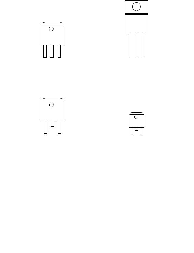
Pin Assignments
FAN1589M
FRONT VIEW
Tab is OUT
1 2 3
GND OUT IN
3-Lead Plastic TO-263
θJC = 3°C/W*
FAN1589MC
FRONT VIEW
Tab is OUT
1 2 3
GND IN
3-Lead Plastic TO-263 Center Cut
θJC = 3°C/W*
FAN1589T
FRONT VIEW
Tab is OUT
1 2 3
GND OUT IN
3-Lead Plastic TO-220
θJC = 3°C/W
FAN1589D
FRONT VIEW
Tab is OUT
1 2 3
GND OUT IN
3-Lead Plastic TO-252
θJC = 3°C/W*
*With package soldered to 0.5 square inch copper area over backside ground plane or internal power plane, ΘJA can vary from 30°C/W to more than 40°C/W. Other mounting techniques can provide a thermal resistance lower than 30°C/W.
Absolute Maximum Ratings
Parameter |
Min. |
Max. |
Unit |
|
|
|
|
VIN |
|
7 |
V |
|
|
|
|
Operating Junction Temperature Range |
0 |
125 |
°C |
|
|
|
|
Storage Temperature Range |
-65 |
150 |
°C |
|
|
|
|
Lead Temperature (Soldering, 10 sec.) |
|
300 |
°C |
|
|
|
|
2 |
REV. 1.0.3 2/25/02 |

PRODUCT SPECIFICATION |
FAN1589 |
|
|
Electrical Characteristics
Tj = 25°C unless otherwise specified.
The • denotes specifications which apply over the specified operating temperature range.
Parameter |
Conditions |
|
Min. |
Typ. |
Max |
Units |
|
|
|
|
|
|
|
Output Voltage |
3.3V ≤ VIN ≤ 7V |
• |
1.176 |
1.200 |
1.224 |
V |
|
10mA ≤ IOUT ≤ 2.7A |
|
|
|
|
|
|
|
|
|
|
|
|
Line Regulation1, 2 |
(VOUT + 1.5V) ≤ VIN ≤ 7V, |
• |
|
0.005 |
0.2 |
% |
|
IOUT = 10mA |
|
|
|
|
|
|
|
|
|
|
|
|
Load Regulation1, 2 |
(VIN – VOUT) = 3V |
• |
|
0.15 |
1.5 |
% |
|
10mA ≤ IOUT ≤ 2.7A |
|
|
|
|
|
|
|
|
|
|
|
|
Dropout Voltage |
∆VREF = 1%, IOUT = 2.7A |
• |
|
1.150 |
1.300 |
V |
|
|
|
|
|
|
|
Current Limit |
(VIN – VOUT) = 2V |
• |
3.1 |
4 |
|
A |
|
|
|
|
|
|
|
Minimum Load Current |
1.5V ≤ (VIN – VOUT) ≤ 5.75V |
• |
10 |
|
|
mA |
|
|
|
|
|
|
|
Quiescent Current |
VIN = 5V |
• |
|
4 |
13 |
mA |
|
|
|
|
|
|
|
Ripple Rejection |
f = 120Hz, COUT = 22 F Tantalum, |
|
60 |
72 |
|
dB |
|
(VIN – VOUT) = 3V, IOUT = 2.7A |
|
|
|
|
|
|
|
|
|
|
|
|
Thermal Regulation |
TA = 25°C, 30ms pulse |
|
|
0.004 |
0.02 |
%/W |
|
|
|
|
|
|
|
Temperature Stability |
|
• |
|
0.5 |
|
% |
|
|
|
|
|
|
|
Long-Term Stability |
TA = 125°C, 1000 hrs. |
|
|
0.03 |
1.0 |
% |
|
|
|
|
|
|
|
RMS Output Noise |
TA = 25°C, 10Hz ≤ f ≤ 10kHz |
|
|
0.003 |
|
% |
(% of VOUT) |
|
|
|
|
|
|
|
|
|
|
|
|
|
Thermal Resistance, |
TO-220 |
|
|
3 |
|
°C/W |
Junction to Case |
|
|
|
|
|
|
TO-263, TO-252 |
|
|
3 |
|
°C/W |
|
|
|
|
|
|||
|
|
|
|
|
|
|
Thermal Shutdown |
|
|
|
150 |
|
°C |
|
|
|
|
|
|
|
Notes:
1.See thermal regulation specifications for changes in output voltage due to heating effects. Load and line regulation are measured at a constant junction temperature by low duty cycle pulse testing.
2.Line and load regulation are guaranteed up to the maximum power dissipation (18W). Power dissipation is determined by input/output differential and the output currrent. Guaranteed maximum output power will not be available over the full input/ output voltage range.
REV. 1.0.3 2/25/02 |
3 |

FAN1589
Typical Performance Characteristics
|
1.5 |
|
|
|
|
|
|
|
1.4 |
|
|
|
|
|
|
(V) |
1.3 |
|
|
|
|
|
|
1.2 |
|
|
|
|
|
|
|
VOLTAGE |
|
|
|
|
|
|
|
1.1 |
|
|
|
|
|
|
|
1.0 |
T=0°C |
|
|
|
|
|
|
DROPOUT |
0.9 |
T=25°C |
|
|
T=125°C |
|
|
0.8 |
|
|
|
|
|||
|
|
|
|
|
|
||
0.7 |
|
|
|
|
|
|
|
|
|
|
|
|
|
|
|
|
0.6 |
|
|
|
|
|
|
|
0.5 |
|
|
|
|
|
|
|
0 |
0.5 |
1 |
1.5 |
2 |
2.5 |
3.0 |
OUTPUT CURRENT (A)
Figure 1. Dropout Voltage vs. Output Current
|
1.225 |
|
|
|
|
|
|
|
|
|
|
|
|
|
|
|
|
|
|
|
|
|
|
|
|
|
1.220 |
|
|
|
|
|
|
|
|
|
|
|
|
|
|
|
|
|
|
|
|
|
|
|
|
(V) |
1.215 |
|
|
|
|
|
|
|
|
|
|
|
|
|
|
|
|
|
|
|
|
|
|
||
|
|
|
|
|
|
|
|
|
|
|
|
|
VOLTAGE |
1.210 |
|
|
|
|
|
|
|
|
|
|
|
|
|
|
|
|
|
|
|
|
|
|
|
|
|
1.205 |
|
|
|
|
|
|
|
|
|
|
|
|
|
|
|
|
|
|
|
|
|
|
|
|
REFERENCE |
1.200 |
|
|
|
|
|
|
|
|
|
|
|
|
|
|
|
|
|
|
|
|
|
|
||
1.195 |
|
|
|
|
|
|
|
|
|
|
|
|
|
|
|
|
|
|
|
|
|
|
|
|
|
|
1.190 |
|
|
|
|
|
|
|
|
|
|
|
|
|
|
|
|
|
|
|
|
|
|
|
|
|
1.185 |
|
|
|
|
|
|
|
|
|
|
|
|
|
|
|
|
|
|
|
|
|
|
|
|
|
1.180 |
|
|
|
|
|
|
|
|
|
|
|
|
|
|
|
|
|
|
|
|
|
|
|
|
|
1.175 |
|
|
|
|
|
|
|
|
|
|
|
|
|
|
|
|
|
|
|
|
|
|
|
|
|
-75 -50 -25 0 25 50 75 100 125 150 175 |
|||||||||||
|
|
|
JUNCTION TEMPERATURE (°C) |
|||||||||
Figure 3. Reference Voltage vs. Temperature
|
5 |
(mA) |
4 |
CURRENT |
3 |
|
|
LOAD |
2 |
MINIMUM |
1 |
|
0 -75 -50 -25 0 25 50 75 100 125 150 175
JUNCTION TEMPERATURE (°C)
Figure 5. Minimum Load Current vs. Temperature
4
PRODUCT SPECIFICATION
|
0.10 |
|
|
|
|
|
|
|
|
|
|
|
|
|
|
|
∆I = 2.7A |
|
|
|
|
|
|
|
|
|
|||
|
|
|
|
|
|
|
|
|
|
|
|
|||
(%) |
0.05 |
|
|
|
|
|
|
|
|
|
|
|
|
|
|
|
|
|
|
|
|
|
|
|
|
|
|
||
DEVIATION |
|
|
|
|
|
|
|
|
|
|
|
|
|
|
0 |
|
|
|
|
|
|
|
|
|
|
|
|
|
|
VOLTAGE |
|
|
|
|
|
|
|
|
|
|
|
|
|
|
-0.10 |
|
|
|
|
|
|
|
|
|
|
|
|
|
|
OUTPUT |
-0.05 |
|
|
|
|
|
|
|
|
|
|
|
|
|
-0.15 |
|
|
|
|
|
|
|
|
|
|
|
|
|
|
|
|
|
|
|
|
|
|
|
|
|
|
|
||
|
|
|
|
|
|
|
|
|
|
|
|
|
|
|
|
-0.20 |
|
|
|
|
|
|
|
|
|
|
|
|
|
|
|
|
|
|
|
|
|
|
|
|
|
|
|
|
|
-75 -50 -25 0 25 50 75 100 125 150 175 |
|||||||||||||
|
|
|
|
JUNCTION TEMPERATURE (°C) |
||||||||||
Figure 2. Load Regulation vs. Temperature
|
1.30 |
|
|
|
|
|
|
|
|
|
|
|
|
|
VOUT SET WITH 1% RESISTORS |
|
|
|
|
||||||||
|
|
|
|
|
|
||||||||
(V) |
1.20 |
|
|
|
|
|
|
|
|
|
|
|
|
|
|
|
|
|
|
|
|
|
|
|
|
||
|
|
|
|
|
|
|
|
|
|
|
|
||
|
|
|
|
|
|
|
|
|
|
|
|
|
|
VOLTAGE |
1.10 |
|
|
|
|
|
|
|
|
|
|
|
|
|
|
|
|
|
|
|
|
|
|
|
|
||
REFERENCE |
|
|
|
|
|
|
|
|
|
|
|
|
|
1.00 |
|
|
|
|
|
|
|
|
|
|
|
|
|
|
|
|
|
|
|
|
|
|
|
|
|
||
|
|
|
|
|
|
|
|
|
|
|
|
|
|
|
0.90 |
|
|
|
|
|
|
|
|
|
|
|
|
|
|
|
|
|
|
|
|
|
|
|
|
|
|
|
|
|
|
|
|
|
|
|
|
|
|
|
|
|
0.80 |
|
|
|
|
|
|
|
|
|
|
|
|
|
|
|
|
|
|
|
|
|
|
|
|
|
|
|
|
|
|
|
|
|
|
|
|
|
|
|
|
|
-75 -50 -25 0 25 50 75 100 125 150 175 |
||||||||||||
|
|
|
JUNCTION TEMPERATURE (°C) |
||||||||||
Figure 4. Output Voltage vs. Temperature
|
5.0 |
(A) |
|
CURRENT |
4.5 |
|
|
CIRCUIT- |
4.0 |
|
|
SHORT |
3.5 |
|
3.0 -75 -50 -25 0 25 50 75 100 125 150 175
JUNCTION TEMPERATURE (°C)
Figure 6. Short-Circuit Current vs. Temperature
REV. 1.0.3 2/25/02
 Loading...