


January 1992
Revised June 1999
DM96S02
Dual Retriggerable Resettable Monostable Multivibrator
General Description |
|
|
an external resistor and capacitor. Resistor values up to 2.0 |
|
The DM96S02 is a dual retriggerable |
and resettable |
MΩ for the DM96S02 reduce required capacitor values. |
||
Hysteresis is provided on the positive trigger input of the |
||||
monostable multivibrator. This one-shot |
provides |
excep- |
||
|
||||
DM96S02 for increased noise immunity.
tionally wide delay range, pulse width stability, predictable accuracy and immunity to noise. The pulse width is set by
Order Code:
Order Number |
Package Number |
Package Description |
|
|
|
DM96S02M |
M16A |
16-Lead Small Outline Integrated Circuit (SOIC), JEDEC MS-012, 0.150 Narrow |
|
|
|
DM96S02N |
N16E |
16-Lead Plastic Dual-In-Line Package (PDIP), JEDEC MS-001, 0.300 Wide |
|
|
|
Devices also available in Tape and Reel. Specify by appending the suffix letter “X” to the ordering code.
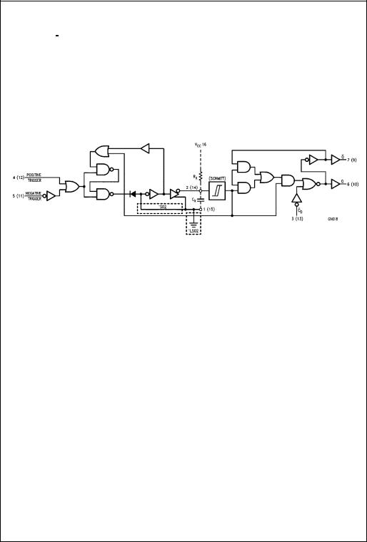
Logic Diagram |
Connection Diagram |
VCC = Pin 16
GND = Pin 8
Pin Descriptions
Pin Names |
Description |
|||
|
|
|
||
|
I0 |
Trigger Input (Active Falling Edge) |
||
|
I1 |
Schmitt Trigger Input (Active Rising-Edge) |
||
|
|
|
Direct Clear Input (Active-LOW) |
|
|
C |
D |
||
|
Q1 - 2 |
True Pulse Output |
||
|
|
|
Complementary Pulse Output |
|
|
Q1 - 2 |
|||
|
CX1, 2 |
External Capacitor Connection |
||
|
RX1,2 |
External Resistor Connection |
||
Triggering Truth Table
|
Pin Number |
|
Operation |
|
|
|
|
||
5(11) |
4(12) |
3(13) |
||
|
||||
|
|
|
|
|
H → L |
L |
H |
Trigger |
|
H |
L → H |
H |
Trigger |
|
X |
X |
L |
Reset |
|
|
|
|
|
H = HIGH Voltage Level ³ VIH
L = LOW Voltage Level £ VIL
X = Immaterial (either H or L)
H ® L = HIGH-to-LOW Voltage Level transition
L ® H = LOW-to-HIGH Voltage Level transition
Multivibrator Monostable Resettable Retriggerable Dual DM96S02
© 1999 Fairchild Semiconductor Corporation |
DS009810.prf |
www.fairchildsemi.com |
DM96S02
Functional Description
The 96S02 dual retriggerable resettable monostable multivibrator has tow DC coupled trigger inputs per function, one active LOW (I0) and one active HIGH (I1). The I1 input utilizes an internal Schmitt trigger with hysteresis of 0.3V to provide increased noise immunity. The use of active HIGH and LOW inputs allows wither rising or falling edge triggering and optional non-retriggerable operation. The inputs are DC coupled making triggering independent of input transition times. When input conditions for triggering are met the Q output goes HIGH and the external capacitor is rapidly discharged and then allowed to recharge. An input
Block Diagram
trigger which occurs during the timing cycle will retrigger the circuit and result in Q remaining HIGH. The output pulse may be terminated (Q to the LOW state) at any time by setting the Direct Clear input LOW. Retriggering may be inhibited by tying the Q output to I0 or the Q output to I1. Differential sensing techniques are used to obtain excellent stability over temperature and power supply variations and a feedback Darlington capacitor discharge circuit minimizes pulse width variation from unit to unit. Schottky TTL output stages provide high switching speeds and output compatibility with all TTL logic families.
www.fairchildsemi.com |
2 |

Operation Notes
TIMING
1.An external resistor (RX) and an external capacitor (CX)
are required as shown in the Logic Diagram. The value of RX may vary from 1.0 kW to 2.0 MW (DM96S02).
2.The value of CX may vary from 0 to any necessary value available. If however, the capacitor has significant leakage relative to VCC/RX the timing equations may not represent the pulse width obtained.
3.Polarized capacitors may be used directly. The (+) ter-
minal of a polarized capacitor is connected to pin 1(15), the (-) terminal to pin 2(14) and RX. Pin 1(15) will remain positive with respect to pin 2(14) during the timing cycle. However, during quiescent (non-triggered) conditions, pin 1(15) may go negative with respect to
pin 2(14) depending on values of RX and VCC. for values of RX ³ 10 kW the maximum amount of capacitor reverse polarity, pin 1(15) negative with respect to pin 2(14) is 500 mV. Most tantalum electrolytic capacitors are rated for safe reverse bias operation up to 5% of their working forward voltage rating; therefore, capaci-
tors having a rating of 10 WVdc or higher should be used with the DM96S02 when RX ³ 10 kW.
4.The output pulse width tW for RX ³ 10 kW and CX ³ 1000 pF is determined as follows:
tW = 0.55 RXCX
Where RX is in kW, CX is in pF, t is in ns or RTX is in kW, CX is in mF, t is in ms.
5.The output pulse width for RX < 10 kW or CX < 1000 pF should be determined from pulse width versus CX or RX graphs.
6.To obtain variable pulse width by remote trimming, the following circuit is recommended:
7.Under any operating condition, CX and RX (Min) must be kept as close to the circuit as possible to minimize stray capacitance and reduce noise pickup.
8.VCC and ground wiring should conform to good high frequency standards so that switching transients on
VCC and ground leads do not cause interaction between one shots. Use of a 0.01 mF to 0.1mF bypass capacitor between VCC and ground located near the circuit is recommended.
TRIGGERING
1.The minimum negative pulse width into I0 is 8.0 ns; the minimum positive pulse width into I1 is 12 ns.
2.Input signals to the DM96S02 exhibiting slow or noisy transitions should use the positive trigger input I1 which contains a Schmitt trigger.
3.When non-retriggerable operation is required, i.e., when input triggers are to be ignored during quasi-sta- ble state, input latching is used to inhibit retriggering.
4.An overriding active LOW level direct clear is provided on each multivibrator. By applying a LOW to the clear, any timing cycle can be terminated or any new cycle inhibited until the LOW reset input is removed. Trigger inputs will not produce spikes in the output when the reset is held LOW. A LOW-to-HIGH transition on CD will not trigger the DM96S02. If the CD input goes HIGH coincident with a trigger transition, the circuit will respond to the trigger.
DM96S02
3 |
www.fairchildsemi.com |
 Loading...