Fairchild Semiconductor DM74LS251N, DM74LS251MX, DM74LS251M, DM74LS251CW Datasheet

August 1986
Revised March 2000
DM74LS251
3-STATE 1-of-8 Line Data Selector/Multiplexer
General Description
These data selectors/multiplexers contain full on-chip binary decoding to select one-of-eight data sources, and feature a strobe-controlled 3-STATE output. The strobe must be at a low logic level to enable these devices. The 3- STATE outputs permit direct connection to a common bus. When the strobe input is HIGH, both outputs are in a highimpedance state in which both the upper and lower transistors of each totem-pole output are OFF, and the output neither drives nor loads the bus significantly. When the strobe is LOW, the outputs are activated and operate as standard TTL totem-pole outputs.
To minimize the possibility that two outputs will attempt to take a common bus to opposite logic levels, the output control circuitry is designed so that the average output disable time is shorter than the average output enable time.
Features
■3-STATE version of DM74LS151
■Interface directly with system bus
■Perform parallel-to-serial conversion
■Permit multiplexing from N-lines to one line
■Complementary outputs provide true and inverted data
■Maximum number of common outputs: 129
■Typical propagation delay time (D to Y): 17 ns
■Typical power dissipation: 35 mW
Ordering Code:
Order Number |
Package Number |
Package Description |
|
|
|
DM74LS251M |
M16A |
16-Lead Small Outline Integrated Circuit (SOIC), JEDEC MS-012, 0.150 Narrow |
|
|
|
DM74LS251N |
N16E |
16-Lead Plastic Dual-In-Line Package (PDIP), JEDEC MS-001, 0.300 Wide |
|
|
|
Devices also available in Tape and Reel. Specify by appending the suffix letter “X” to the ordering code.
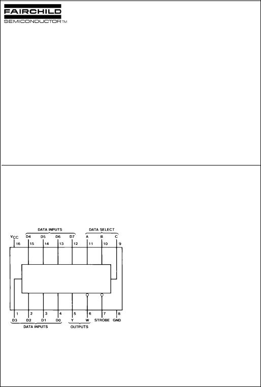
Connection Diagram |
Function Table |
|
|
|
|
|||
|
|
|
|
|
|
|
|
|
|
|
|
|
Inputs |
|
Outputs |
|
|
|
|
|
|
|
|
|
|
|
|
|
|
Select |
|
Strobe |
Y |
W |
|
|
|
|
|
|
|
|
||
|
|
C |
B |
A |
S |
|
||
|
|
|
|
|
||||
|
|
|
|
|
|
|
|
|
|
|
X |
X |
X |
H |
Z |
Z |
|
|
|
L |
L |
L |
L |
D0 |
|
|
|
|
D0 |
|
|||||
|
|
L |
L |
H |
L |
D1 |
|
|
|
|
D1 |
|
|||||
|
|
L |
H |
L |
L |
D2 |
|
|
|
|
D2 |
|
|||||
|
|
L |
H |
H |
L |
D3 |
|
|
|
|
D3 |
|
|||||
|
|
H |
L |
L |
L |
D4 |
|
|
|
|
D4 |
|
|||||
|
|
H |
L |
H |
L |
D5 |
|
|
|
|
D5 |
|
|||||
|
|
H |
H |
L |
L |
D6 |
|
|
|
|
D6 |
|
|||||
|
|
H |
H |
H |
L |
D7 |
|
|
|
|
D7 |
|
|||||
|
|
|
|
|
|
|
|
|
|
H |
= HIGH Logic Level |
|
|
|
|
|
|
|
L = LOW Logic Level |
|
|
|
|
|
||
|
X = Don't Care |
|
|
|
|
|
||
|
Z = High Impedance (OFF) |
|
|
|
|
|||
|
D0, D1…D7 = The level of the respective D input |
|
|
|
||||
Selector/Multiplexer Data Line 8-of-1 STATE-3 DM74LS251
© 2000 Fairchild Semiconductor Corporation |
DS006415 |
www.fairchildsemi.com |

DM74LS251
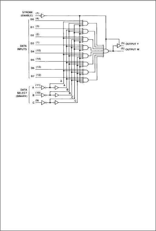
Logic Diagram
www.fairchildsemi.com |
2 |
 Loading...