Fairchild Semiconductor DM74LS175SJX, DM74LS175SJ, DM74LS175N, DM74LS175MX, DM74LS175CW Datasheet

August 1992
Revised April 2000
DM74LS174 • DM74LS175
Hex/Quad D-Type Flip-Flops with Clear
General Description
These positive-edge-triggered flip-flops utilize TTL circuitry to implement D-type flip-flop logic. All have a direct clear input, and the quad (175) versions feature complementary outputs from each flip-flop.
Information at the D inputs meeting the setup time requirements is transferred to the Q outputs on the positive-going edge of the clock pulse. Clock triggering occurs at a particular voltage level and is not directly related to the transition time of the positive-going pulse. When the clock input is at either the HIGH or LOW level, the D input signal has no effect at the output.
Features
■DM74LS174 contains six flip-flops with single-rail outputs
■DM74LS175 contains four flip-flops with double-rail outputs
■Buffered clock and direct clear inputs
■Individual data input to each flip-flop
■Applications include:
Buffer/storage registers
Shift registers
Pattern generators
■Typical clock frequency 40 MHz
■Typical power dissipation per flip-flop 14 mW
Ordering Code:
Order Number |
Package Number |
Package Description |
|
|
|
DM74LS174M |
M16A |
16-Lead Small Outline Integrated Circuit (SOIC), JEDEC MS-012, 0.150 Narrow |
|
|
|
DM74LS174SJ |
M16D |
16-Lead Small Outline Package (SOP), EIAJ TYPE II, 5.3mm Wide |
|
|
|
DM74LS174N |
N16E |
16-Lead Plastic Dual-In-Line Package (PDIP), JEDEC MS-001, 0.300 Wide |
|
|
|
DM74LS175M |
M16A |
16-Lead Small Outline Integrated Circuit (SOIC), JEDEC MS-012, 0.150 Narrow |
|
|
|
DM74LS175SJ |
M16D |
16-Lead Small Outline Package (SOP), EIAJ TYPE II, 5.3mm Wide |
|
|
|
DM74LS175N |
N16E |
16-Lead Plastic Dual-In-Line Package (PDIP), JEDEC MS-001, 0.300 Wide |
|
|
|
Devices also available in Tape and Reel. Specify by appending the suffix letter “X” to the ordering code.
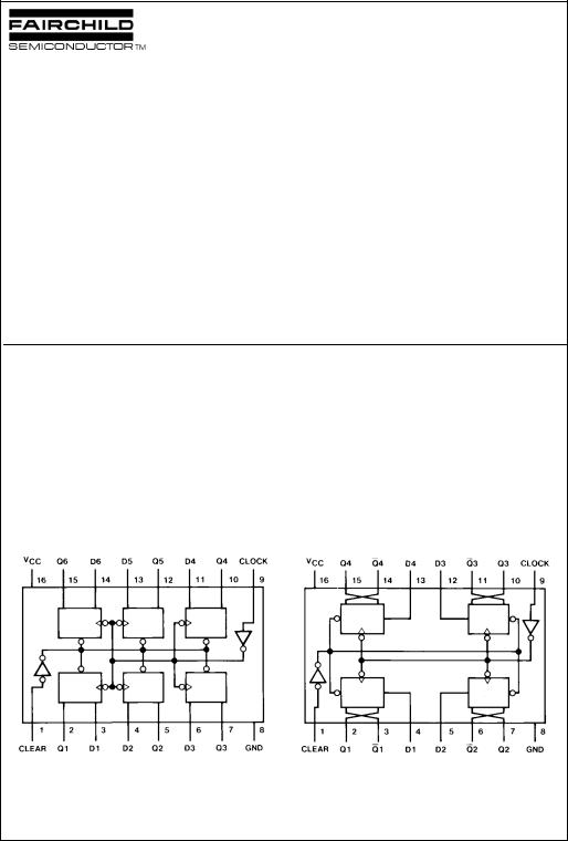
Connection Diagrams
DM74LS174 DM74LS175
Clear with Flops-Flip Type-D Hex/Quad DM74LS175 • DM74LS174
© 2000 Fairchild Semiconductor Corporation |
DS006404 |
www.fairchildsemi.com |

DM74LS174 • DM74LS175
Function Table
(Each Flip-Flop)
|
Inputs |
|
|
Outputs |
||||
|
|
|
|
|
|
|
|
|
|
|
|
|
|
|
|
|
|
Clear |
Clock |
D |
Q |
|
Q † |
|||
|
|
|
|
|
|
|
||
L |
X |
X |
L |
|
|
H |
||
H |
− |
H |
H |
|
|
L |
||
H |
− |
L |
L |
|
|
H |
||
H |
L |
X |
Q0 |
|
|
|
||
|
|
Q |
0 |
|||||
H = HIGH Level (steady state) L = LOW Level (steady state) X = Don’t Care
− = Transition from LOW-to-HIGH level
Q0 = The level of Q before the indicated steady-state input conditions were established.
† = DM74LS175 only
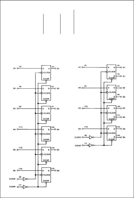
Logic Diagrams
DM74LS174 |
DM74LS175 |
www.fairchildsemi.com |
2 |

Absolute Maximum Ratings(Note 1)
Supply Voltage |
7V |
Note 1: The “Absolute Maximum Ratings” are those values beyond which |
|
the safety of the device cannot be guaranteed. The device should not be |
|||
Input Voltage |
7V |
operated at these limits. The parametric values defined in the Electrical |
|
Characteristics tables are not guaranteed at the absolute maximum ratings. |
|||
Operating Free Air Temperature Range |
0°C to +70°C |
||
The “Recommended Operating Conditions” table will define the conditions |
|||
Storage Temperature Range |
−65°C to +150°C |
for actual device operation. |
|
|
DM74LS174 Recommended Operating Conditions
Symbol |
Parameter |
|
Min |
Nom |
Max |
Units |
VCC |
Supply Voltage |
|
4.75 |
5 |
5.25 |
V |
VIH |
HIGH Level Input Voltage |
|
2 |
|
|
V |
VIL |
LOW Level Input Voltage |
|
|
|
0.8 |
V |
IOH |
HIGH Level Output Current |
|
|
|
−0.4 |
mA |
IOL |
LOW Level Output Current |
|
|
|
8 |
mA |
fCLK |
Clock Frequency (Note 2) |
|
0 |
|
30 |
MHz |
fCLK |
Clock Frequency (Note 3) |
|
0 |
|
25 |
MHz |
tW |
Pulse Width |
Clock |
20 |
|
|
ns |
|
(Note 4) |
Clear |
20 |
|
|
|
|
|
|
|
|||
|
|
|
|
|
|
|
tSU |
Data Setup Time (Note 4) |
|
20 |
|
|
ns |
tH |
Data Hold Time (Note 4) |
|
0 |
|
|
ns |
tREL |
Clear Release Time (Note 4) |
|
25 |
|
|
ns |
TA |
Free Air Operating Temperature |
0 |
|
70 |
°C |
|
Note 2: CL = 15 pF, RL = 2 kΩ, TA = 25°C and VCC = 5V.
Note 3: CL = 50 pF, RL = 2 kΩ, TA = 25°C and VCC = 5V.
Note 4: TA = 25°C and VCC = 5V.
DM74LS174 Electrical Characteristics
over recommended operating free air temperature range (unless otherwise noted)
Symbol |
Parameter |
Conditions |
Min |
Typ |
Max |
Units |
|
(Note 5) |
|||||||
|
|
|
|
|
|
||
|
|
|
|
|
|
|
|
VI |
Input Clamp Voltage |
VCC = Min, II = −18 mA |
|
|
−1.5 |
V |
|
VOH |
HIGH Level |
VCC = Min, IOH = Max |
2.7 |
3.4 |
|
V |
|
|
Output Voltage |
VIL = Max, VIH = Min |
|
||||
|
|
|
|
|
|||
VOL |
LOW Level |
VCC = Min, IOL = Max |
|
0.35 |
0.5 |
|
|
|
Output Voltage |
VIL = Max, VIH = Min |
|
V |
|||
|
|
|
|
||||
|
|
IOL = 4 mA, VCC = Min |
|
0.25 |
0.4 |
|
|
II |
Input Current @ Max Input Voltage |
VCC = Max, VI = 7V |
|
|
0.1 |
mA |
|
IIH |
HIGH Level Input Current |
VCC = Max, VI = 2.7V |
|
|
20 |
μA |
|
IIL |
LOW Level |
VCC = Max |
Clock |
|
−0.4 |
|
|
|
Input Current |
VI = 0.4V |
Clear |
|
−0.4 |
mA |
|
|
|
|
Data |
|
−0.36 |
|
|
|
|
|
|
|
|
|
|
IOS |
Short Circuit Output Current |
VCC = Max (Note 6) |
−20 |
|
−100 |
mA |
|
ICC |
Supply Current |
VCC = Max (Note 7) |
|
16 |
26 |
mA |
Note 5: All typicals are at VCC = 5V, TA = 25°C.
Note 6: Not more than one output should be shorted at a time, and the duration should not exceed one second.
Note 7: With all outputs OPEN and 4.5V applied to all data and clear inputs, ICC is measured after a momentary ground, then 4.5V applied to the clock.
DM74LS175 • DM74LS174
3 |
www.fairchildsemi.com |
 Loading...