


March 1988
Revised March 2000
DM74LS574
Octal D-Type Flip-Flop with 3-STATE Outputs
General Description
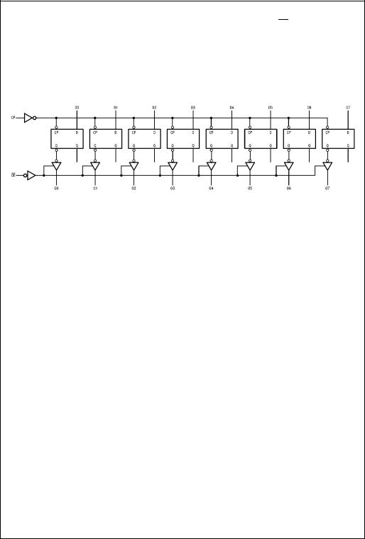
The DM74LS574 is a high speed low power octal flip-flop with a buffered common Clock (CP) and a buffered common Output Enable (OE). The information presented to the D inputs is stored in the flip-flops on the LOW-to-HIGH Clock (CP) transition.
This device is functionally identical to the DM74LS374 except for the pinouts.
Ordering Code:
Order Number |
Package Number |
Package Description |
|
|
|
DM74LS574WM |
M20B |
20-Lead Small Outline Integrated Circuit (SOIC), JEDEC MS-013, 0.300 Wide |
|
|
|
DM74LS574N |
N20A |
20-Lead Plastic Dual-In-Line Package (PDIP), JEDEC MS-001, 0.300 Wide |
|
|
|
Devices also available in Tape and Reel. Specify by appending the suffix letter “X” to the ordering code.
Logic Symbol |
Connection Diagram |
VCC = Pin 20
GND = Pin 10
Truth Table
|
Inputs |
|
Outputs |
Dn |
CP |
OE |
On |
|
|
|
|
H |
|
L |
H |
L |
|
L |
L |
X |
X |
H |
Z |
H = HIGH Voltage Level
L = LOW Voltage Level X = Immaterial
Z = High Impedance
= HIGH-to-LOW Clock (CP) transition
Outputs STATE-3 with Flop-Flip Type-D Octal DM74LS574
© 2000 Fairchild Semiconductor Corporation |
DS009815 |
www.fairchildsemi.com |
DM74LS574
Functional Description
The DM74LS574 consists of eight edge-triggered flip-flops with individual D-type inputs and 3-STATE true outputs. The buffered clock and buffered Outputs Enable are common to all flip-flops. The eight flip-flops will store the state of their individual D inputs that meet the setup and hold times requirements on the LOW-to-HIGH Clock (CP) tran-
Logic Diagram
sition. With the Output Enable (OE) LOW, the contents of the eight flip-flops are available at the outputs. When the OE is HIGH, the outputs go to the high impedance state. Operation of the OE input does not affect the state of the flip-flops.
www.fairchildsemi.com |
2 |
 Loading...