


DM74LS221SJX
Fairchild Semiconductor DM74LS221SJX, DM74LS221SJ, DM74LS221N, DM74LS221MX, DM74LS221M Datasheet
...
© 2000 Fairchild Semiconductor Corporation DS006409 www.fairchildsemi.com
August 1986
Revised April 2000
DM74LS221 Dual Non-Retriggerable One-Shot with Clear and Complementary Outputs
DM74LS221 Dual Non-Retriggerable One-Shot
with Clear and Complementary Outputs
General Description
The DM74LS221 is a dual monostable multivibrator with
Schmitt-trigger input. E ach devi ce has three inp uts permi t-
ting the choice of either leading-edge or trailing-e dge trig-
gering. Pin (A) is an active-LOW trigger transition input and
pin (B) is an active-HI GH transition Schmitt-trigger input
that allows jitter free triggering for inputs with transition
rates as slow as 1 volt/second. This provides the input with
excellent noise immunity. Additionally an internal latching
circuit at the input stage also provid es a high immunity to
V
CC
noise. The clear (CLR) input can terminate the output
pulse at a predetermined tim e independent of the timing
components. This (CLR) input also serves as a trigger
input when it is pulsed with a low level pulse transition
(
). To obtain the best and trouble free operatio n from
this device please read operati ng ru les as well as th e Fair-
child Semiconductor one-shot application notes carefully
and observe recommendations.
Features
■ A dual, highly stable one-shot
■ Compensated for V
CC
and temperature variations
■ Pin-out identical to DM74LS123 (Note 1)
■ Output pulse width range from 30 ns to 70 seconds
■ Hysteresis provided at (B) input for added noise
immunity
■ Direct reset terminates output pulse
■ Triggerable from CLEAR input
■ DTL, TTL compatible
■ Input clamp diodes
Note 1: The pin-out is identical to DM74LS123 but, functionally it is not;
refer to Operating R ules #10 in this datasheet .
Ordering Code:
Devices also availab le in Tape and Reel. Specify by appending th e s uffix let t er “X” to the ordering code.
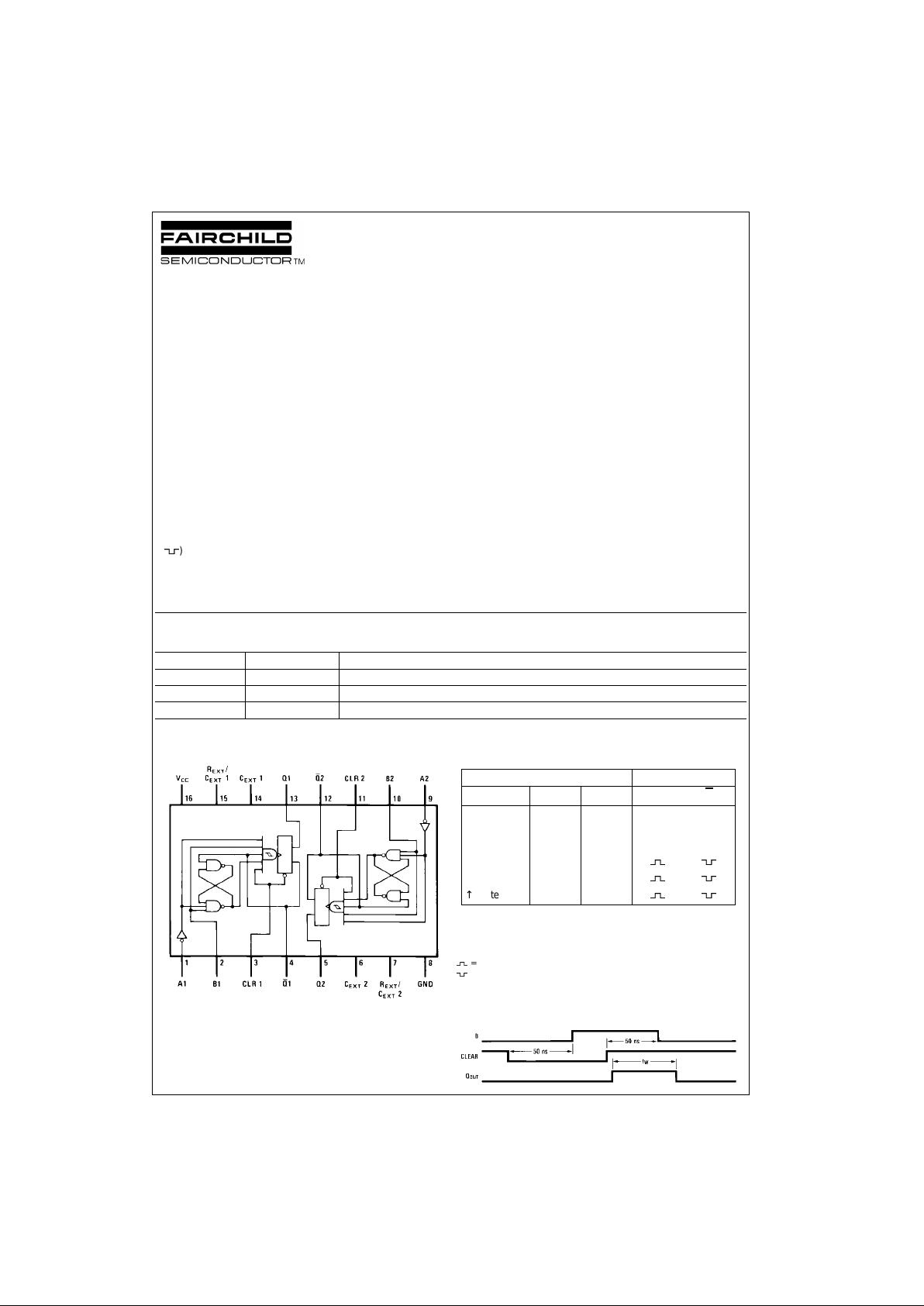
Connection Diagram Function Table
H = HIGH Logic Level
L = LOW Logic Level
X = Can Be Either LOW or HIGH
↑ = Positive Going Transition
↓ = Negative Going Trans it ion
= A Positive Pulse
= A Negative Pulse
Note 2: This mode of triggering requires first the B input be set from a
LOW-to-HIGH leve l while the CLEAR input is m aintained at logic LOW
level. Then with the B in put at logic HIGH level , the CLEAR input whos e
positive transition fro m LOW-to-HIGH will trigger an output pulse.
Order Number Package Number Package Description
DM74LS221M M16A 16-Lead Small Outline Integrat ed Circuit (SOIC), JEDEC MS-012, 0.150 Narrow
DM74LS221SJ M16D 16-Lead Small Out line Package (SOP), EIAJ TYPE II, 5.3mm Wide
DM74LS221N N16E 16-Lead Plastic Dual-In-Line Package (PDIP), JEDEC MS-001, 0.300 Wide
Inputs Outputs
CLEAR A B Q Q
LXXLH
XHXLH
XXLLH
HL↑
H ↓ H
↑ (Note 2) L H

www.fairchildsemi.com 2
DM74LS221 Dual Non-Retriggerable One-Shot
Functional Description
The basic output pulse width is determined by selection of
an external resistor (R
X
) and capacitor (C
X
). Once trig-
gered, the basic puls e w idth is independent of f urt her i np ut
transitions and is a functio n of the timing compon ents, or it
may be reduced or termin ated by use of the active low
CLEAR input. Stable output pulse width ranging from 30 ns
to 70 seconds is readily obtainable.
Operating Rules
1. An external resistor (R
X
) and an external capacitor
(C
X
) are required for prop er op er ati on . Th e val u e of C
X
may vary from 0 to approxima tely 1000 µF. For small
time constants h igh-grade mica, glass, polyp ropylene,
polycarbonate, or polystyrene material capacitor may
be used. For large time c onst ant s use ta nta lum or spe -
cial aluminum capacitor s. If timing capacitor has leak-
ages approaching 10 0 nA or if stray capacit ance from
either terminal to gr ound is gr eater than 5 0 pF the tim -
ing equations may not repre sent the pulse width the
device generates.
2. When an electrol ytic capa ci to r is us ed for C
X
a switch-
ing diode is often requir ed for standard TTL one-shots
to prevent high inverse leakage current . Thi s switchin g
diode is not need ed for the DM7 4LS221 one- shot and
should not be used.
Furthermore, if a polarized timing capacitor is used on
the DM74LS221, the positive side of the capacitor
should be connected to the “C
EXT
” pin (Figure 1).
3. For C
X
>> 1000 pF, the output pulse width (t
W
) is
defined as follows:
t
W
= KR
X
C
X
where [R
X
is in kΩ]
[C
X
is in pF]
[t
W
is in ns]
K ≈ Ln2 = 0.70
4. The multiplicative factor K is plotted as a function of C
X
for design considerations: (See Figure 4).
5. For C
X
< 1000 pF see F igure 3 for t
W
vs. C
X
family
curves with R
X
as a parameter.
6. To obtain variable pulse widths by remote trim ming,
the following circuit is recommended: (See Figure 2).
7. Output pulse width versus V
CC
and temperatures: Fig-
ure 5 depicts the relationship between pulse width vari-
ation versu s V
CC
. Figure 6 depicts pulse width variation
versus temperatures.
8. Duty cycle is defined as t
W
/T × 100 in percentage, if it
goes above 50% the output pulse width will become
shorter. If the duty cycle varies between LOW and
HIGH values, this causes out put pulse w idth to var y, or
jitter (a function of the R
EXT
only). To reduce jitter, R
EXT
should be as large as possible, for example, with
R
EXT
= 100k jitter is not appreciable until the duty cycle
approaches 90%.
9. Under any operating condition C
X
and R
X
must be kept
as close to the one-shot device pins as possible to min-
imize stray capacitance, to reduce noise pick-up, and
to reduce I-R and Ldi/d t voltage devel oped along th eir
connecting paths. If the lead leng th from C
X
to pins (6)
and (7) or pins (14) an d (15) is greate r than 3 cm, for
example, the output pulse width might be quite different
from values predicte d from the appropriat e equations.
A non-inductive and low capacitive path is necessary to
ensure complete discharge of C
X
in each cycle of its
operation so that the output pulse width will b e accu-
rate.
10. Although the DM74LS221's pin-out is id entical to the
DM74LS123 it should be remembered that they are not
functionally identica l. The DM74LS123 is a retrigger-
able device such that the output is dependent upon the
input transitions when its output “Q” is at the “High”
state. Furthermore, it is recommended for the
DM74LS123 to externally ground the C
EXT
pin for
improved system performance. However, this pin on
the DM74LS221 is not an int ernal connection to the
device gro un d. He nc e , if s u bst i tu tion of an DM 74LS221
onto an DM74LS123 d esi g n la yout w he re the C
EXT
pin
is wired to the ground, the device will not function.
11. V
CC
and ground wiring shoul d conform to good high-
frequency standards and practices so that switching
transients on the V
CC
and ground return leads do not
cause interaction between one-shots. A 0.01 µF to 0.10
µF bypass capacitor (disk ce ramic or monolithic type)
from V
CC
to ground is necessar y on each de vice. Fur-
thermore, the bypass capacitor sho uld be located as
close to the V
CC
-pin as spac e permits.
3 www.fairchildsemi.com
DM74LS221 Dual Non-Retriggerable One-Shot
Operating Rules (Continued)
FIGURE 1.
Note: “R
remote
” should be as close to th e one-shot as possible.
FIGURE 2.
FIGURE 3.
FIGURE 4.
FIGURE 5. FIGURE 6.
Note: For further detailed dev ic e c haracteristics and output performance, pleas e refer to the Fairchild Sem ic onductor one-shot ap plication note AN-372.
 Loading...