


Fairchild Semiconductor DM74LS273WMX, DM74LS273WM, DM74LS273SJX, DM74LS273SJ, DM74LS273N Datasheet
...
October 1988
Revised March 2000
DM74LS273
8-Bit Register with Clear
General Description
The DM74LS273 is a high speed 8-bit register, consisting of eight D-type flip-flops with a common Clock and an asynchronous active LOW Master Reset. This device is supplied in a 20-pin package featuring 0.3 inch row spacing.
Features
■Edge-triggered
■8-bit high speed register
■Parallel in and out
■Common clock and master reset
Ordering Code:
Order Number |
Package Number |
Package Description |
|
|
|
DM74LS273WM |
M20B |
20-Lead Small Outline Integrated Circuit (SOIC), JEDEC MS-013, 0.300 Wide |
|
|
|
DM74LS273SJ |
M20D |
20-Lead Small Outline Package (SOP), EIAJ TYPE II, 5.3mm Wide |
|
|
|
DM74LS273N |
N20A |
20-Lead Plastic Dual-In-Line Package (PDIP), JEDEC MS-001, 0.300 Wide |
|
|
|
Devices also available in Tape and Reel. Specify by appending the suffix letter “X” to the ordering code.
Logic Symbol |
Connection Diagram |
VCC = Pin 20
GND = Pin 10
|
Pin Descriptions |
Truth Table |
|
|
|
|||
|
|
|
|
|
|
|
|
|
|
Pin Names |
Description |
|
|
Inputs |
|
Outputs |
|
|
|
|
|
|
|
|||
|
|
|
|
MR |
CP |
Dn |
Qn |
|
|
CP |
Clock Pulse Input (Active Rising Edge) |
||||||
|
D0–D7 |
Data Inputs |
|
L |
X |
X |
L |
|
|
|
Asynchronous Master Reset Input (Active LOW) |
|
H |
|
H |
H |
|
|
MR |
|
||||||
Q0–Q7 |
Flip-Flop Outputs |
|
H |
|
L |
L |
||
|
|
|
|
H |
= HIGH Voltage Level |
|
|
|
|
|
|
|
|
|
|
||
|
|
|
|
L = LOW Voltage Level |
|
|
|
|
|
|
|
|
X = Immaterial |
|
|
|
|
Clear with Register Bit-8 DM74LS273
© 2000 Fairchild Semiconductor Corporation |
DS009825 |
www.fairchildsemi.com |
DM74LS273
Functional Description
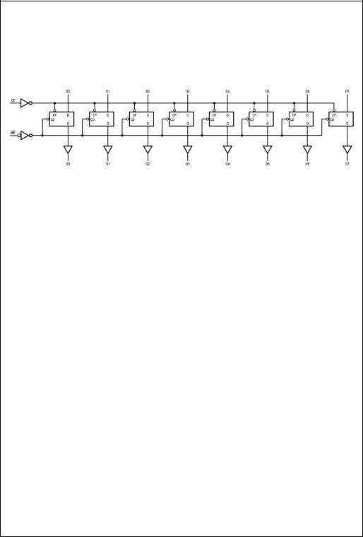
The DM74LS273 is an 8-bit parallel register with a common Clock and common Master Reset. When the MR input is LOW, the Q outputs are LOW, independent of the other inputs. Information meeting the setup and hold time requirements of the D inputs is transferred to the Q outputs on the LOW-to-HIGH transition of the clock input.
Logic Diagram
www.fairchildsemi.com |
2 |
 Loading...