


DM9334N

© 2000 Fairchild Semiconductor Corporation DS006609 www.fairchildsemi.com
August 1986
Revised February 2000
DM9334 8-Bit Addressable Latch
DM9334
8-Bit Addressable Latch
General Description
The DM9334 is a high speed 8-bit Addressable Latch
designed for general purpose storage applications in digital
systems. It is a multifunct ional device capable of storing
single line data in ei ght addressable latche s, and being a
one-of-eight decoder and demultiplexer with active level
HIGH outputs. The device also incorporates an active level
LOW common clear for resetting all latches, as well as an
active level LOW enable.
The DM9334 has four modes of operation which are shown
in the mode selection table. In the addressable latch mode,
data on the data line (D) is written into the addressed latch.
The addressed latch will follow the data input with all no n-
addressed latches remaining in their previous states. In the
memory mode, all latches remain in their previous sta te
and are unaffected by the data or address inputs.
In the one-of-eight decoding or demultiplexing mode, the
addressed output will follow the state of the D input with all
other inputs in the LOW state. In the clear mode all outputs
are LOW and unaffected by the address and data inputs.
When operating the device as an addressable latch,
changing more than on e bit of th e addre ss could i mpos e a
transient wrong address. Therefore, this should only be
done while in the memory mode.
The function tables summarize the operation of the prod-
uct.
Features
■ Common clear
■ Easily expandable
■ Random (addressable) data entry
■ Serial to parallel capability
■ 8 bits of storage/output of each bit available
■ Active high demultiplexing/decoding capability
Ordering Code:
Connection Diagram
Order Number Package Number Package Description
DM9334N N16E 16-Lead Plastic Dual-In-Line Package (PDIP), JEDEC MS-001, 0.300 Wide
www.fairchildsemi.com 2
DM9334
Function Tables
H = HIGH Voltage Level
L = LOW Voltage Level
X = Don’t Care Condition
Q
N−1
= Previous Output St at e
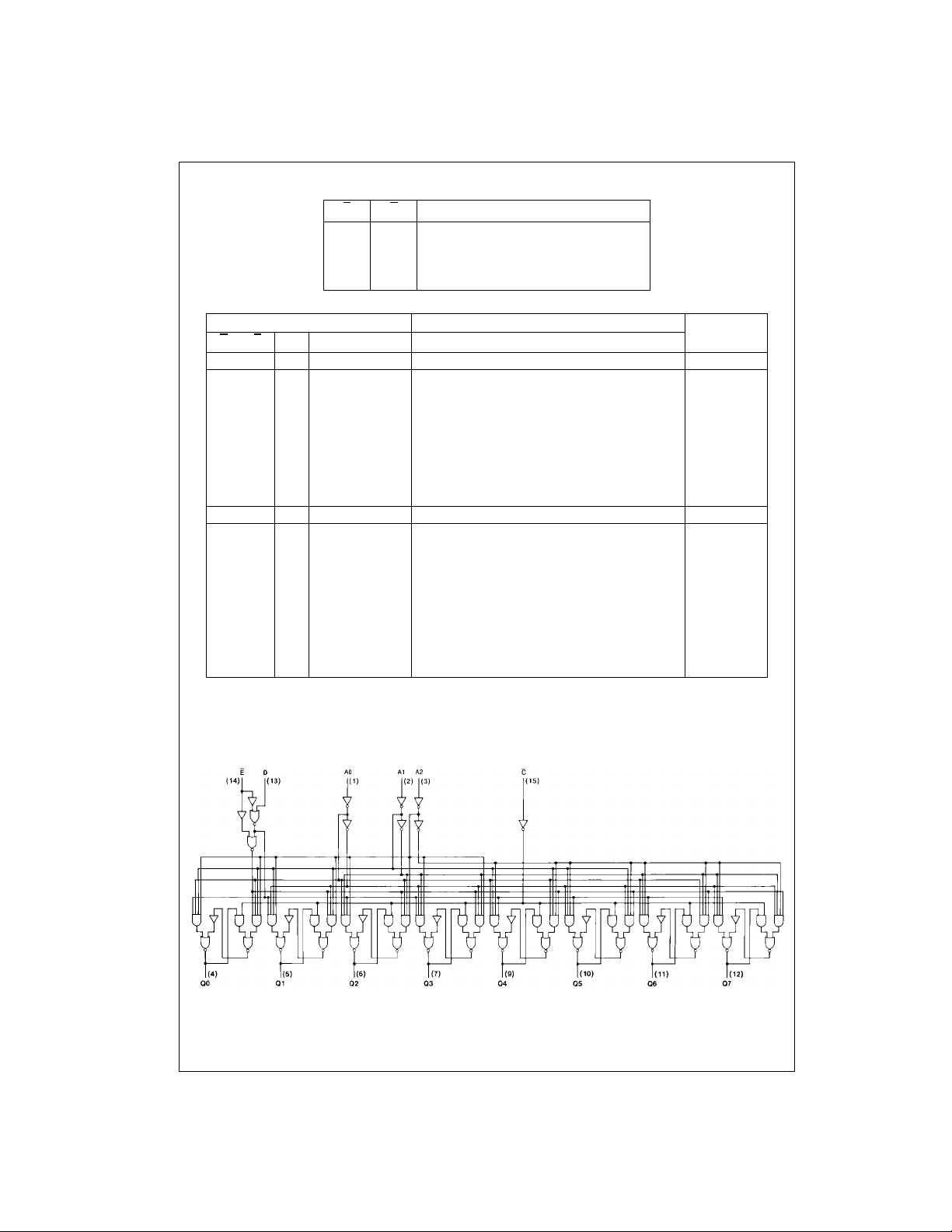
Logic Diagram
E C Mode
L H Addressable Latch
H H Memory
L L Active HIGH Eight Channel Demultiplexer
H L Clear
Inputs Present Output States
Mode
C
E D A0A1A2Q0Q1Q2Q3Q4Q5Q6Q7
LHXXXXLLLLLLLL Clear
LLLLLLLLLLLLLL
Demultiplex
LLHLLLHLLLLLLL
LLLHLLLLLLLLLL
LLHHLLLHLLLLLL
••• • •
••• • •
••• • •
LLHHHHLLLLLLLH
HHXXXXQ
N−1
Memory
HLLLLLLQ
N−1
Q
N−1
Q
N−1
Addressable
Latch
HLHLLLHQ
N−1
Q
N−1
HLLHLLQ
N−1
LQ
N−1
HLHHLLQ
N−1
HQ
N−1
••• • •
••• • •
••• • •
HLLHHHQ
N−1
Q
N−1
L
HLHHHHQ
N−1
Q
N−1
H
 Loading...