Fairchild Semiconductor DM74LS194AN, DM74LS194AMX, DM74LS194AM Datasheet

August 1986
Revised March 2000
DM74LS194A
4-Bit Bidirectional Universal Shift Register
General Description
This bidirectional shift register is designed to incorporate virtually all of the features a system designer may want in a shift register; they feature parallel inputs, parallel outputs, right-shift and left-shift serial inputs, operating-mode-con- trol inputs, and a direct overriding clear line. The register has four distinct modes of operation, namely:
Parallel (broadside) load
Shift right (in the direction QA toward QD)
Shift left (in the direction QD toward QA)
Inhibit clock (do nothing)
Features
■Parallel inputs and outputs
■Four operating modes: Synchronous parallel load Right shift
Left shift Do nothing
■Positive edge-triggered clocking
■Direct overriding clear
Synchronous parallel loading is accomplished by applying the four bits of data and taking both mode control inputs, S0 and S1, HIGH. The data is loaded into the associated flip-flops and appear at the outputs after the positive transition of the clock input. During loading, serial data flow is inhibited.
Shift right is accomplished synchronously with the rising edge of the clock pulse when S0 is HIGH and S1 is LOW. Serial data for this mode is entered at the shift-right data input. When S0 is LOW and S1 is HIGH, data shifts left synchronously and new data is entered at the shift-left serial input.
Clocking of the flip-flop is inhibited when both mode control inputs are LOW.
Ordering Code:
Order Number |
Package Number |
Package Description |
|
|
|
DM74LS194AM |
M16A |
16-Lead Small Outline Integrated Circuit (SOIC), JEDEC MS-012, 0.150 Narrow |
|
|
|
DM74LS194AN |
N16E |
16-Lead Plastic Dual-In-Line Package (PDIP), JEDEC MS-001, 0.300 Wide |
|
|
|
Devices also available in Tape and Reel. Specify by appending the suffix letter “X” to the ordering code.
Connection Diagram
Register Shift Universal Bidirectional Bit-4 DM74LS194A
© 2000 Fairchild Semiconductor Corporation |
DS006407 |
www.fairchildsemi.com |

DM74LS194A
Function Table
|
|
|
|
|
Inputs |
|
|
|
Outputs |
|
|
|
|
|
|
|
|
|
|
|
|
||
Clear |
Mode |
Clock |
|
Serial |
Parallel |
QA |
QB |
QC |
QD |
||
|
|
|
|
|
|
||||||
S1 |
S0 |
|
Left |
Right |
A B C D |
||||||
|
|
|
|
|
|
|
|||||
|
|
|
|
|
|
|
|
|
|
|
|
L |
X |
X |
X |
X |
X |
X X X X |
L |
L |
L |
L |
|
H |
X |
X |
L |
X |
X |
X X X X |
QA0 |
QB0 |
QC0 |
QD0 |
|
H |
H |
H |
− |
X |
X |
a b c d |
a |
b |
c |
d |
|
H |
L |
H |
− |
X |
H |
X X X X |
H |
QAn |
QBn |
QCn |
|
H |
L |
H |
− |
X |
L |
X X X X |
L |
QAn |
QBn |
QCn |
|
H |
H |
L |
− |
H |
X |
X X X X |
QBn |
QCn |
QDn |
H |
|
H |
H |
L |
− |
L |
X |
X X X X |
QBn |
QCn |
QDn |
L |
|
H |
L |
L |
X |
X |
X |
X X X X |
QA0 |
QB0 |
QC0 |
QD0 |
|
H = HIGH Level (steady state) L = LOW Level (steady state)
X = Don’t Care (any input, including transitions) − = Transition from LOW-to-HIGH level
a, b, c, d = The level of steady state input at inputs A, B, C or D, respectively.
QA0, QB0, QC0, QD0 = The level of QA, QB, QC, or QD, respectively, before the indicated steady state input conditions were established. QAn, QBn, QCn, QDn = The level of QA, QB, QC, respectively, before the most-recent − transition of the clock.
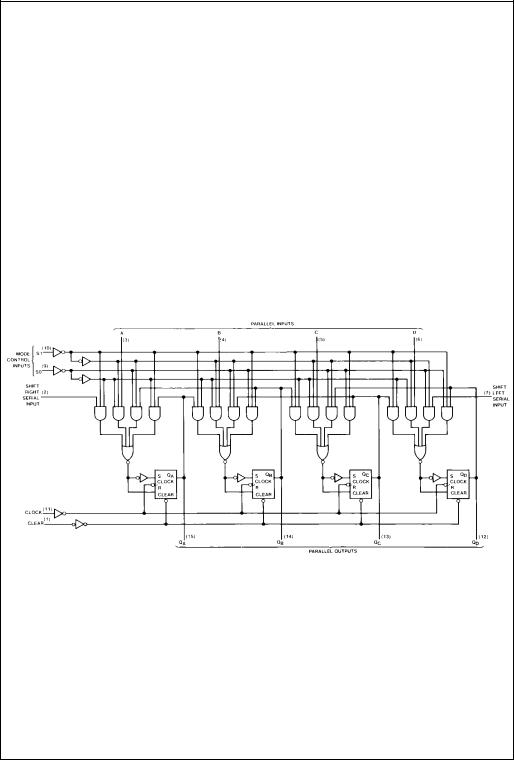
Logic Diagram
www.fairchildsemi.com |
2 |
 Loading...