Fairchild Semiconductor DM74LS90N, DM74LS90MX, DM74LS90M, DM74LS90CW Datasheet

August 1986
Revised March 2000
DM74LS90
Decade and Binary Counters
General Description
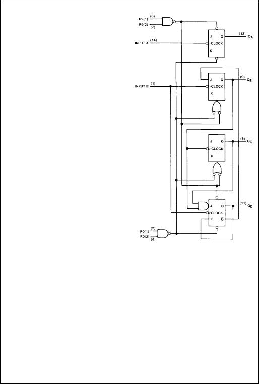
Each of these monolithic counters contains four masterslave flip-flops and additional gating to provide a divide-by- two counter and a three-stage binary counter for which the count cycle length is divide-by-five for the DM74LS90.
All of these counters have a gated zero reset and the DM74LS90 also has gated set-to-nine inputs for use in BCD nine’s complement applications.
To use their maximum count length (decade or four bit binary), the B input is connected to the QA output. The input count pulses are applied to input A and the outputs are as described in the appropriate truth table. A symmetrical divide-by-ten count can be obtained from the DM74LS90 counters by connecting the QD output to the A input and applying the input count to the B input which gives a divide-by-ten square wave at output QA.
Features
■Typical power dissipation 45 mW
■Count frequency 42 MHz
Ordering Code:
Order Number |
Package Number |
Package Description |
|
|
|
DM74LS90M |
M14A |
14-Lead Small Outline Integrated Circuit (SOIC), JEDEC MS-120, 0.150 Narrow |
|
|
|
DM74LS90N |
N14A |
14-Lead Plastic Dual-In-Line Package (PDIP), JEDEC MS-001, 0.300 Wide |
|
|
|
Devices also available in Tape and Reel. Specify by appending the suffix letter “X” to the ordering code.
Connection Diagram |
Reset/Count Truth Table |
|
|
|
|||||
|
|
|
|
|
|
|
|
||
|
|
|
Reset Inputs |
|
|
Output |
|
||
|
|
|
|
|
|
|
|
|
|
|
|
R0(1) |
R0(2) |
R9(1) |
R9(2) |
QD |
QC |
QB |
QA |
|
|
H |
H |
L |
X |
L |
L |
L |
L |
|
|
H |
H |
X |
L |
L |
L |
L |
L |
|
|
X |
X |
H |
H |
H |
L |
L |
H |
|
|
X |
L |
X |
L |
|
COUNT |
|
|
|
|
L |
X |
L |
X |
|
COUNT |
|
|
|
|
L |
X |
X |
L |
|
COUNT |
|
|
|
|
X |
L |
L |
X |
|
COUNT |
|
|
|
|
|
|
|
|
|
|
|
|
Counters Binary and Decade DM74LS90
© 2000 Fairchild Semiconductor Corporation |
DS006381 |
www.fairchildsemi.com |

DM74LS90
Function Tables
BCD Count Sequence (Note 1)
Count |
|
|
Output |
|
|
|
|
|
|
|
QD |
QC |
QB |
QA |
0 |
L |
L |
L |
L |
1 |
L |
L |
L |
H |
2 |
L |
L |
H |
L |
3 |
L |
L |
H |
H |
4 |
L |
H |
L |
L |
5 |
L |
H |
L |
H |
6 |
L |
H |
H |
L |
7 |
L |
H |
H |
H |
8 |
H |
L |
L |
L |
9 |
H |
L |
L |
H |
|
|
|
||
|
Bi-Quinary (5-2) (Note 2) |
|
||
|
|
|
|
|
Count |
|
|
Output |
|
|
|
|
|
|
|
QA |
QD |
QC |
QB |
0 |
L |
L |
L |
L |
1 |
L |
L |
L |
H |
2 |
L |
L |
H |
L |
3 |
L |
L |
H |
H |
4 |
L |
H |
L |
L |
5 |
H |
L |
L |
L |
6 |
H |
L |
L |
H |
7 |
H |
L |
H |
L |
8 |
H |
L |
H |
H |
9 |
H |
H |
L |
L |
|
|
|
|
|
H = HIGH Level
L = LOW Level
X = Don’t Care
Note 1: Output QA is connected to input B for BCD count.
Note 2: Output QD is connected to input A for bi-quinary count.
Note 3: Output QA is connected to input B.
Logic Diagram
The J and K inputs shown without connection are for reference only and are functionally at a high level.
www.fairchildsemi.com |
2 |
 Loading...