


DM74LS27N
© 2000 Fairchild Semiconductor Corporation DS006359 www.fairchildsemi.com
May 1986
Revised March 2000
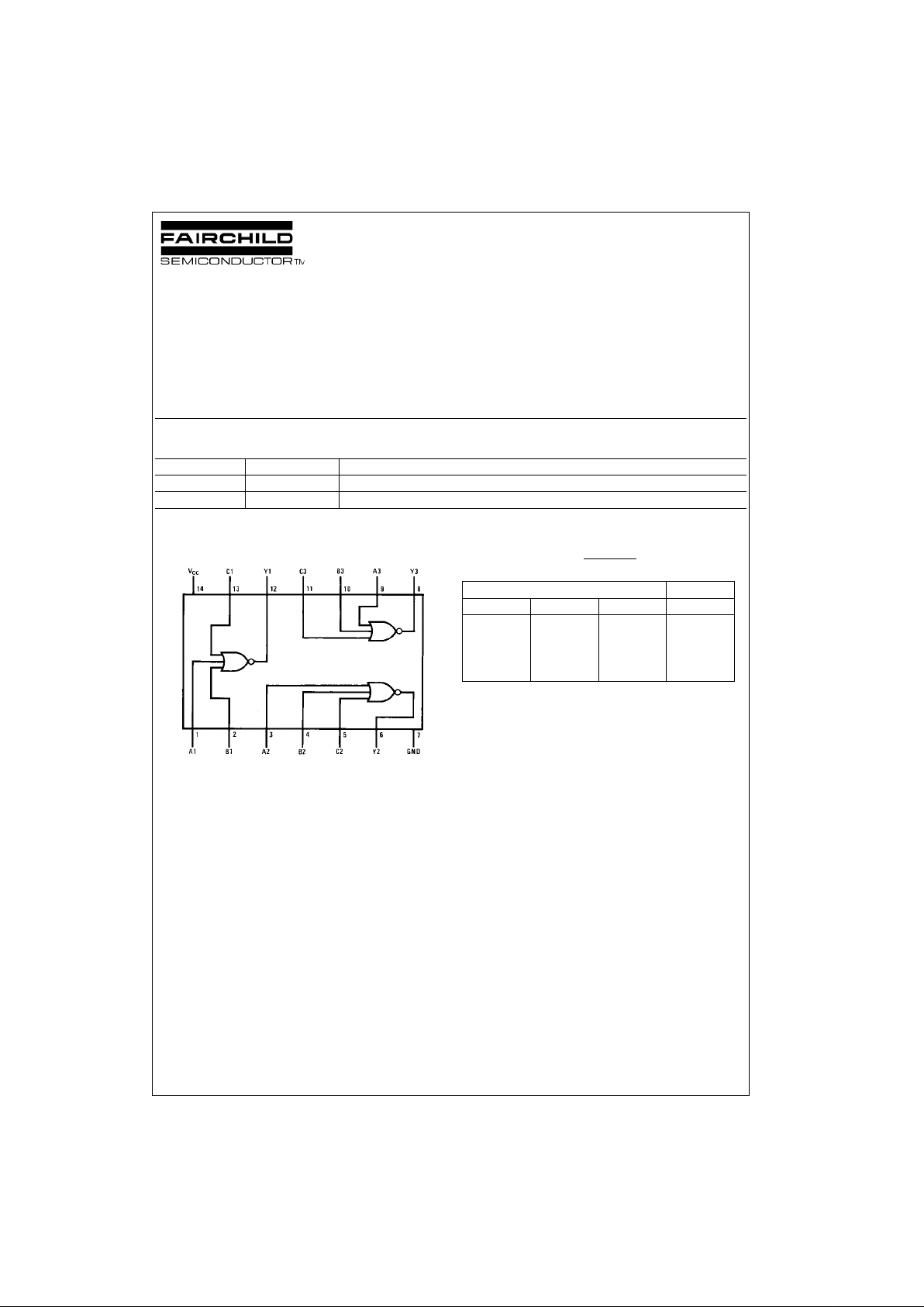
DM74LS27 Trip le 3-Input NOR Gate
DM74LS27
Triple 3-Input NOR Gate
General Description
This device contains three independent gates each of
which performs the logic NOR function.
Ordering Code:
Devices also availab le in Tape and Reel. Specify by appending th e s uffix let t er “X” to the ordering code.
Connection Diagram Function Table
H = HIGH Logic Level
L = LOW Logic Level
X = Either LOW or HIGH Logic Level
Order Number Package Number Package Description
DM74LS27M M14A 14-Lead Small Outline Integrated Circuit (SOIC), JEDEC MS-120, 0.150 Narrow
DM74LS27N N14A 14-Lead Plastic Dual-In-Line Package (PDIP), JEDEC MS-001, 0.300 Wide
Y = A + B + C
Inputs Output
ABCY
LLLH
XXHL
XHXL
HXXL
www.fairchildsemi.com 2
DM74LS27
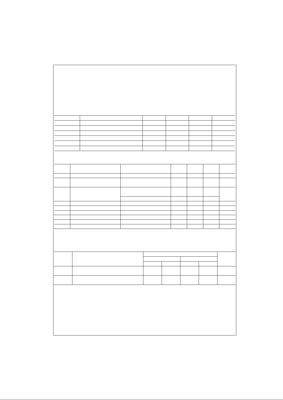
Absolute Maximum Ratings(Note 1)
Note 1: The “Absolute Maximum Ratings” are those values beyond which
the safety of the dev ice cannot be guaranteed. T he device sh ould not be
operated at these limits. The parametric values defined in the Electrical
Characteristics tables are not guaranteed at the absolute maximum ratings.
The “Recommend ed O peratin g Cond itions” t able w ill defin e the co ndition s
for actual device operation.
Recommended Operating Conditions
Electrical Characteristics
over recommended operating free air temperature range (unless otherwise noted)
Note 2: All typicals are at V
CC
= 5V, T
A
= 25°C.
Note 3: Not more than one output should be shorted at a time, and the duration should not exceed one second.
Switching Characteristics
at V
CC
= 5V and T
A
= 25°C
Supply Voltage 7V
Input Voltage 7V
Operating Free Air Temperature Range 0°C to +70°C
Storage Temperature Range −65°C to +150°C
Symbol Parameter Min Nom Max Units
V
CC
Supply Voltage 4.75 5 5. 25 V
V
IH
HIGH Level Input Voltage 2 V
V
IL
LOW Level Input Voltage 0.8 V
I
OH
HIGH Level Output Current −0.4 mA
I
OL
LOW Level Output Current 8 mA
T
A
Free Air Operating Temperature 0 70 °C
Symbol Parameter Conditions Min
Typ
Max Units
(Note 2)
V
I
Input Clamp Voltage V
CC
= Min, I
I
= −18 mA −1.5 V
V
OH
HIGH Level V
CC
= Min, I
OH
= Max,
2.7 3.4 V
Output Voltage V
IL
= Max
V
OL
LOW Level V
CC
= Min, I
OL
= Max,
0.35 0.5
Output Voltage V
IH
= Min V
I
OL
= 4 mA, V
CC
= Min 0.25 0.4
I
I
Input Current @ Max Input Voltage V
CC
= Max, V
I
= 7V 0.1 mA
I
IH
HIGH Level Input Current V
CC
= Max, V
I
= 2.7V 20 µA
I
IL
LOW Level Input Current V
CC
= Max, V
I
= 0.4V −0.36 mA
I
OS
Short Circuit Output Current V
CC
= Max (Note 3) −20 −100 mA
I
CCH
Supply Current with Outputs HIGH V
CC
= Max 2 4 mA
I
CCL
Supply Current with Outputs LOW V
CC
= Max 3.4 6.8 mA
Symbol Parameter
R
L
= 2 kΩ
Units
C
L
= 15 pF C
L
= 50 pF
Min Max Min Max
t
PLH
Propagation Delay Time
313518ns
LOW-to-HIGH Level Output
t
PHL
Propagation Delay Time
310415ns
HIGH-to-LOW Level Output
 Loading...