


SGS Thomson Microelectronics LD1086V120, LD1086V, LD1086DT90, LD1086DT80, LD1086DT50 Datasheet
...
|
LD1086 |
|
SERIES |
|
1.5A LOW DROP FIXED AND ADJUSTABLE |
|
POSITIVE VOLTAGE REGULATORS |
■TYPICAL DROPOUT VOLTAGE 1.3V AT 1.5A
■THREE TERMINAL ADJUSTABLE OR FIXED OUTPUT VOLATGE 1.8V, 2.5V, 2.85V, 3.3V, 3.6V, 5V, 8V, 9V, 12V
■GUARANTEED OUTPUT CURRENT UP TO 1.5A
■OUTPUT TOLERANCE ±1% AT 25oC AND
±2% IN FULL TEMPERATURE RANGE
■INTERNAL POWER AND THERMAL LIMIT
■WIDE OPERATING TEMPERATURE RANGE -40oC TO 125oC
■PACKAGE AVAILABLE: TO-220, D2PAK, D2PAK/A, DPAK,
■PINOUT COMPATIBILITY WITH STANDARD ADJUSTABLE VOLTAGE REGULATORS
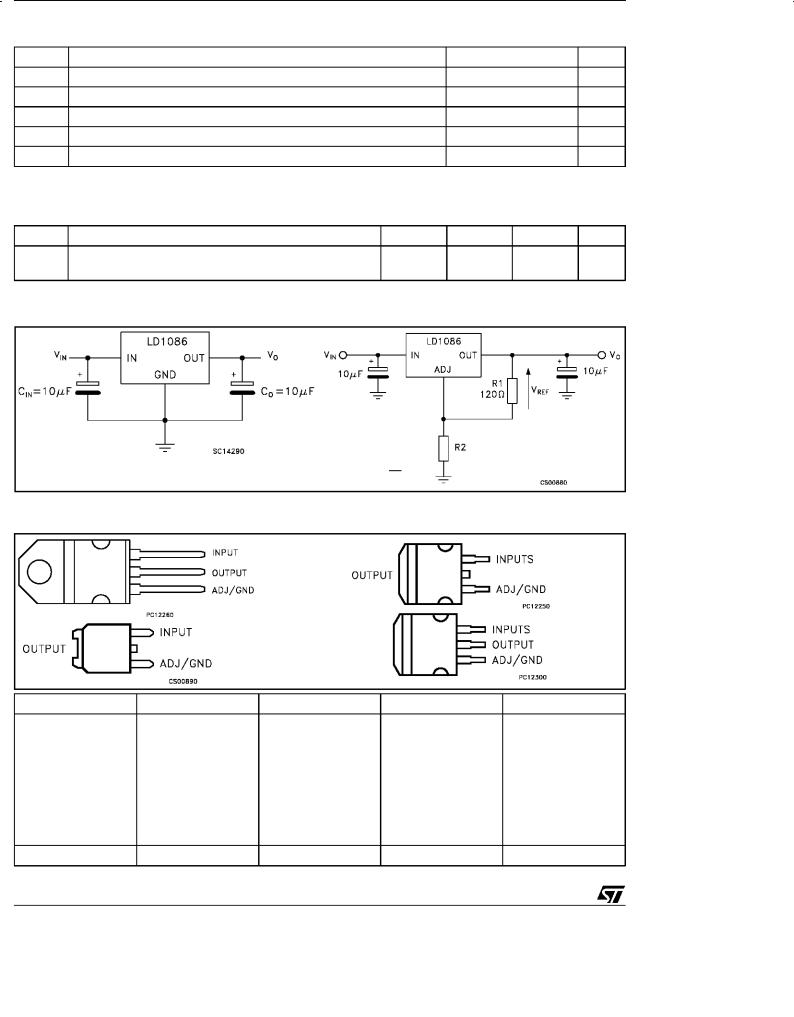
DESCRIPTION
D2PAK/A
TO-220
D2PAK
DPAK (TO-252)
The LD1086 is a LOW DROP Voltage Regulator able to provide up to 1.5A of Output Current. Dropout is guaranteed at a maximum of 1.5V at the maximum output current, decreasing at lower loads. The LD1086 is a pin compatible with older 3-terminal adjustable regulators, but has better performances in term of drop and output tolerance. A 2.85V output version is suitable for SCSI-2 active termination. Unlike PNP regulators, where a part of the output
current is wasted as quiescent current, the LD1086 quiescent current flow into the load, so increase efficency. Only a 10 μF minimum capacitor is needed for stability. The device is supplied in TO-220, D2PAK, D2PAK/A and DPAK packages. On chip trimming allows the regulator to reach a very tight output voltage tolerance, within ± 1% at 25 oC.
BLOCK DIAGRAM
May 2000 |
1/17 |
LD1086 SERIES
ABSOLUTE MAXIMUM RATINGS
Symbol |
Parameter |
Value |
Unit |
||
VIN |
DC Input Voltage |
|
30 |
|
V |
IOUT |
Output Current |
Internally |
Limited |
mA |
|
Pto t |
Power Dissipation |
Internally |
Limited |
mW |
|
Tstg |
Storage Temperature Range |
-50 |
to |
150 |
o C |
To p |
Operating Junction Temperature Range |
-40 |
to |
125 |
o C |
Absolute Maximum Ratings are those value beyond which damage to the device may occur. Functional operation under these condition is not implied. Over the above suggested Max Power Dissipation a Short Circuit could definetively damage the device.
THERMAL DATA
Symbol |
Parameter |
TO-220 |
D2PAK |
DPAK |
Unit |
Rthjca se |
Thermal Resistance Junction-case |
3 |
3 |
8 |
oC/W |
Rthjamb |
Thermal Resistance Junction-ambient |
50 |
62.5 |
|
oC/W |
APPLICATION CIRCUIT FOR FIXED AND ADJUSTABLE VERSION
VO = VREF (1 + R2)
R1
CONNECTION DIAGRAM AND ORDERING NUMBERS (top view)
TO-220 |
D2PAK |
|
|
|
DPAK |
|
D2PAK/A |
TO-220 |
D2PAK (**) |
D2PAK/A (**) |
DPAK (**) |
Output Voltage |
LD1086V18 |
LD1086D2T18 |
LD1086D2M18 |
LD1086DT18 |
1.8V |
LD1086V25 |
LD1086D2T25 |
LD1086D2M25 |
LD1086DT25 |
2.5V |
LD1086V28 |
LD1086D2T28 |
LD1086D2M28 |
LD1086DT28 |
2.85V |
LD1086V33 |
LD1086D2T33 |
LD1086D2M33 |
LD1086DT33 |
3.3V |
LD1086V36 |
LD1086D2T36 |
LD1086D2M36 |
LD1086DT36 |
3.6V |
LD1086V50 |
LD1086D2T50 |
LD1086D2M50 |
LD1086DT50 |
5V |
LD1086V80 |
LD1086D2T80 |
LD1086D2M80 |
LD1086DT80 |
8V |
LD1086V90 |
LD1086D2T90 |
LD1086D2M90 |
LD1086DT90 |
9V |
LD1086V120 |
LD1086D2T120 |
LD1086D2M120 |
LD1086DT120 |
12V |
LD1086V |
LD1086D2T |
LD1086D2M |
LD1086DT |
1.25 to 28V |
(**) Available in Tape & Reel with the suffix ºTRº.
2/17
LD1086 SERIES
ELECTRICAL CHARACTERISTICS FOR LD1086#18 (refer to the test circuits, |
|
|
|
|||||
Tj = -40 to 125 oC, VIN = 4.8 V, |
CIN = CO = 10 μF unless otherwise specified) |
|
|
|
||||
Symbol |
Parameter |
|
Test Conditions |
Min. |
Typ. |
Max. |
Unit |
|
VO |
Output Voltage |
IO = 0 mA |
Tj = 25 oC |
1.782 |
1.8 |
1.818 |
V |
|
VO |
Output Voltage (Note 1) |
IO = 0 to 1.5 A |
VIN = 3.4 to 30 V |
1.764 |
1.8 |
1.836 |
V |
|
VO |
Line Regulation |
VIN = 3.4 to 18 V |
IO = 0 mA Tj = 25 oC |
|
0.2 |
4 |
mV |
|
VO |
Line Regulation |
VIN = 3.4 to 18 V |
IO = 0 mA |
|
0.4 |
4 |
mV |
|
VO |
Load Regulation |
IO = 0 to 1.5 A |
Tj = 25 oC |
|
0.5 |
8 |
mV |
|
VO |
Load Regulation |
IO = 0 to 1.5 A |
|
|
1 |
16 |
mV |
|
Vd |
Dropout Voltage |
IO = 1.5 A |
|
|
|
1.3 |
1.5 |
V |
Id |
Quiescent Current |
VIN ≤ 30 V |
|
|
|
5 |
10 |
mA |
ISC |
Short Circuit Current |
VIN - VO = 5V |
|
1.5 |
2 |
|
A |
|
|
|
VIN - VO = 25V |
|
0.05 |
0.2 |
|
|
|
|
Thermal Regulation |
Ta = 25 oC |
30ms Pulse |
|
0.01 |
0.04 |
%/W |
|
SVR |
Supply Voltage Rejection |
IO =1.5 A |
f = 120 Hz CO = 25μF |
60 |
82 |
|
dB |
|
|
|
VIN = 6.8 ± 3V |
|
|
|
|
|
|
eN |
Output Noise Voltage |
B = 10Hz to 10KHz Ta = 25 oC |
|
0.003 |
|
% |
||
S |
Temperature Stability |
|
|
|
|
0.5 |
|
% |
S |
Long Term Stability |
1000 hrs Ta = 125 oC |
|
0.5 |
|
% |
||
Note1: See short-circuit curve for available output current at fixed dropout.
ELECTRICAL CHARACTERISTICS FOR LD1086#25 (refer to the test circuits, |
|
|
|
|||||
Tj = -40 to 125 oC, VIN = 5.5 V, |
CIN = CO = 10 μF unless otherwise specified) |
|
|
|
||||
Symbol |
Parameter |
|
Test Conditions |
Min. |
Typ. |
Max. |
Unit |
|
VO |
Output Voltage |
IO = 0 mA |
Tj = 25 oC |
2.475 |
2.5 |
2.525 |
V |
|
VO |
Output Voltage (Note 1) |
IO = 0 to 1.5 A |
VIN = 4.1 to 30 V |
2.45 |
2.5 |
2.55 |
V |
|
VO |
Line Regulation |
VIN = 4.1 to 18 V |
IO = 0 mA Tj = 25 oC |
|
0.2 |
5 |
mV |
|
VO |
Line Regulation |
VIN = 4.1 to 18 V |
IO = 0 mA |
|
0.4 |
5 |
mV |
|
VO |
Load Regulation |
IO = 0 to 1.5 A |
Tj = 25 oC |
|
0.5 |
10 |
mV |
|
VO |
Load Regulation |
IO = 0 to 1.5 A |
|
|
1 |
18 |
mV |
|
Vd |
Dropout Voltage |
IO = 1.5 A |
|
|
|
1.3 |
1.5 |
V |
Id |
Quiescent Current |
VIN ≤ 30 V |
|
|
|
5 |
10 |
mA |
ISC |
Short Circuit Current |
VIN - VO = 5V |
|
1.5 |
2 |
|
A |
|
|
|
VIN - VO = 25V |
|
0.05 |
0.2 |
|
|
|
|
Thermal Regulation |
Ta = 25 oC |
30ms Pulse |
|
0.01 |
0.04 |
%/W |
|
SVR |
Supply Voltage Rejection |
IO = 1.5 A |
f = 120 Hz CO = 25μF |
60 |
81 |
|
dB |
|
|
|
VIN = 7.5 ± 3V |
|
|
|
|
|
|
eN |
Output Noise Voltage |
B = 10Hz to 10KHz Ta = 25 oC |
|
0.003 |
|
% |
||
S |
Temperature Stability |
|
|
|
|
0.5 |
|
% |
S |
Long Term Stability |
1000 hrs Ta = 125 oC |
|
0.5 |
|
% |
||
Note1: See short-circuit curve for available output current at fixed dropout.
3/17

LD1086 SERIES
ELECTRICAL CHARACTERISTICS FOR LD1086#285 (refer to the test circuits, |
|
|
|
|||||
Tj = -40 to 125 oC, VIN = 5.85 V, |
CIN = CO = 10 μF unless otherwise specified) |
|
|
|
||||
Symbol |
Parameter |
|
Test Conditions |
Min. |
Typ. |
Max. |
Unit |
|
VO |
Output Voltage |
IO = 0 mA |
Tj = 25 oC |
2.821 |
2.85 |
2.879 |
V |
|
VO |
Output Voltage (Note 1) |
IO = 0 to 1.5 A |
VIN = 4.5 to 30 V |
2.793 |
2.85 |
2.907 |
V |
|
VO |
Line Regulation |
VIN = 4.5 to 18 V |
IO = 0 mA Tj = 25 oC |
|
0.2 |
6 |
mV |
|
VO |
Line Regulation |
VIN = 4.5 to 18 V |
IO = 0 mA |
|
0.5 |
6 |
mV |
|
VO |
Load Regulation |
IO = 0 to 1.5 A |
Tj = 25 oC |
|
1 |
12 |
mV |
|
VO |
Load Regulation |
IO = 0 to 1.5 A |
|
|
2 |
20 |
mV |
|
Vd |
Dropout Voltage |
IO = 1.5 A |
|
|
|
1.3 |
1.5 |
V |
Id |
Quiescent Current |
VIN ≤ 30 V |
|
|
|
5 |
10 |
mA |
ISC |
Short Circuit Current |
VIN - VO = 5V |
|
1.5 |
2 |
|
A |
|
|
|
VIN - VO = 25V |
|
0.05 |
0.2 |
|
|
|
|
Thermal Regulation |
Ta = 25 oC |
30ms Pulse |
|
0.01 |
0.04 |
%/W |
|
SVR |
Supply Voltage Rejection |
IO = 1.5 A |
f = 120 Hz CO = 25μF |
60 |
80 |
|
dB |
|
|
|
VIN = 7.85 ± 3V |
|
|
|
|
|
|
eN |
Output Noise Voltage |
B = 10Hz to 10KHz Ta = 25 oC |
|
0.003 |
|
% |
||
S |
Temperature Stability |
|
|
|
|
0.5 |
|
% |
S |
Long Term Stability |
1000 hrs Ta = 125 oC |
|
0.5 |
|
% |
||
Note1: See short-circuit curve for available output current at fixed dropout.
ELECTRICAL CHARACTERISTICS FOR LD1086#33 (refer to the test circuits, |
|
|
|
|||||
Tj = -40 to 125 oC, VIN = 6.3 V, |
CIN = CO = 10 μF unless otherwise specified) |
|
|
|
||||
Symbol |
Parameter |
|
Test Conditions |
Min. |
Typ. |
Max. |
Unit |
|
VO |
Output Voltage |
IO = 0 mA |
Tj = 25 oC |
3.267 |
3.3 |
3.333 |
V |
|
VO |
Output Voltage (Note 1) |
IO = 0 to 1.5 A |
VIN = 4.9 to 30 V |
3.234 |
3.3 |
3.366 |
V |
|
VO |
Line Regulation |
VIN = 4.9 to 18 V |
IO = 0 mA Tj = 25 oC |
|
0.5 |
10 |
mV |
|
VO |
Line Regulation |
VIN = 4.9 to 18 V |
IO = 0 mA |
|
1 |
10 |
mV |
|
VO |
Load Regulation |
IO = 0 to 1.5 A |
Tj = 25 oC |
|
3 |
15 |
mV |
|
VO |
Load Regulation |
IO = 0 to 1.5 A |
|
|
7 |
25 |
mV |
|
Vd |
Dropout Voltage |
IO = 1.5 A |
|
|
|
1.3 |
1.5 |
V |
Id |
Quiescent Current |
VIN ≤ 30 V |
|
|
|
5 |
10 |
mA |
ISC |
Short Circuit Current |
VIN - VO = 5V |
|
1.5 |
2 |
|
A |
|
|
|
VIN - VO = 25V |
|
0.05 |
0.2 |
|
|
|
|
Thermal Regulation |
Ta = 25 oC |
30ms Pulse |
|
0.01 |
0.04 |
%/W |
|
SVR |
Supply Voltage Rejection |
IO = 1.5 A |
f = 120 Hz CO = 25μF |
60 |
79 |
|
dB |
|
|
|
VIN = 8.3 ± 3V |
|
|
|
|
|
|
eN |
Output Noise Voltage |
B = 10Hz to 10KHz Ta = 25 oC |
|
0.003 |
|
% |
||
S |
Temperature Stability |
|
|
|
|
0.5 |
|
% |
S |
Long Term Stability |
1000 hrs Ta = 125 oC |
|
0.5 |
|
% |
||
Note1: See short-circuit curve for available output current at fixed dropout.
4/17

LD1086 SERIES
ELECTRICAL CHARACTERISTICS FOR LD1086#36 (refer to the test circuits, |
|
|
|
|||||
Tj = -40 to 125 oC, VIN = 6.6 V, |
CIN = CO = 10 μF unless otherwise specified) |
|
|
|
||||
Symbol |
Parameter |
|
Test Conditions |
Min. |
Typ. |
Max. |
Unit |
|
VO |
Output Voltage |
IO = 0 mA |
Tj = 25 oC |
3.564 |
3.6 |
3.636 |
V |
|
VO |
Output Voltage (Note 1) |
IO = 0 to 1.5 A |
VIN = 5.2 to 30 V |
3.528 |
3.6 |
3.672 |
V |
|
VO |
Line Regulation |
VIN = 5.2 to 18 V |
IO = 0 mA Tj = 25 oC |
|
0.5 |
10 |
mV |
|
VO |
Line Regulation |
VIN = 5.2 to 18 V |
IO = 0 mA |
|
1 |
10 |
mV |
|
VO |
Load Regulation |
IO = 0 to 1.5 A |
Tj = 25 oC |
|
3 |
15 |
mV |
|
VO |
Load Regulation |
IO = 0 to 1.5 A |
|
|
7 |
25 |
mV |
|
Vd |
Dropout Voltage |
IO = 1.5 A |
|
|
|
1.3 |
1.5 |
V |
Id |
Quiescent Current |
VIN ≤ 30 V |
|
|
|
5 |
10 |
mA |
ISC |
Short Circuit Current |
VIN - VO = 5V |
|
1.5 |
2 |
|
A |
|
|
|
VIN - VO = 25V |
|
0.05 |
0.2 |
|
|
|
|
Thermal Regulation |
Ta = 25 oC |
30ms Pulse |
|
0.01 |
0.04 |
%/W |
|
SVR |
Supply Voltage Rejection |
IO = 1.5 A |
f = 120 Hz CO = 25μF |
60 |
78 |
|
dB |
|
|
|
VIN = 8.6 ± 3V |
|
|
|
|
|
|
eN |
Output Noise Voltage |
B = 10Hz to 10KHz Ta = 25 oC |
|
0.003 |
|
% |
||
S |
Temperature Stability |
|
|
|
|
0.5 |
|
% |
S |
Long Term Stability |
1000 hrs Ta = 125 oC |
|
0.5 |
|
% |
||
Note1: See short-circuit curve for available output current at fixed dropout.
ELECTRICAL CHARACTERISTICS FOR LD1086#50 (refer to the test circuits, Tj = -40 to 125 oC, VIN = 8 V, CIN = CO = 10 μF unless otherwise specified)
Symbol |
Parameter |
|
Test Conditions |
Min. |
Typ. |
Max. |
Unit |
|
VO |
Output Voltage |
IO = 0 mA |
Tj = 25 oC |
4.95 |
5 |
5.05 |
V |
|
VO |
Output Voltage (Note 1) |
IO = 0 to 1.5 A |
VIN = 6.6 to 30 V |
4.9 |
5 |
5.1 |
V |
|
VO |
Line Regulation |
VIN = 6.6 to 20 V |
IO = 0 mA Tj = 25 oC |
|
0.5 |
10 |
mV |
|
VO |
Line Regulation |
VIN = 6.6 to 20 V |
IO = 0 mA |
|
1 |
10 |
mV |
|
VO |
Load Regulation |
IO = 0 to 1.5 A |
Tj = 25 oC |
|
5 |
20 |
mV |
|
VO |
Load Regulation |
IO = 0 to 1.5 A |
|
|
10 |
35 |
mV |
|
Vd |
Dropout Voltage |
IO = 1.5 A |
|
|
|
1.3 |
1.5 |
V |
Id |
Quiescent Current |
VIN ≤ 30 V |
|
|
|
5 |
10 |
mA |
ISC |
Short Circuit Current |
VIN - VO = 5V |
|
1.5 |
2 |
|
A |
|
|
|
VIN - VO = 25V |
|
0.05 |
0.2 |
|
|
|
|
Thermal Regulation |
Ta = 25 oC |
30ms Pulse |
|
0.01 |
0.04 |
%/W |
|
SVR |
Supply Voltage Rejection |
IO = 1.5 A |
f = 120 Hz CO = 25μF |
60 |
75 |
|
dB |
|
|
|
VIN = 10 ± 3V |
|
|
|
|
|
|
eN |
Output Noise Voltage |
B = 10Hz to 10KHz Ta = 25 oC |
|
0.003 |
|
% |
||
S |
Temperature Stability |
|
|
|
|
0.5 |
|
% |
S |
Long Term Stability |
1000 hrs Ta = 125 oC |
|
0.5 |
|
% |
||
Note1: See short-circuit curve for available output current at fixed dropout.
5/17
LD1086 SERIES
ELECTRICAL CHARACTERISTICS FOR LD1086#80 (refer to the test circuits, Tj = -40 to 125 oC, VIN = 11 V, CIN = CO = 10 μF unless otherwise specified)
Symbol |
Parameter |
|
Test Conditions |
Min. |
Typ. |
Max. |
Unit |
|
VO |
Output Voltage |
IO = 0 mA |
Tj = 25 oC |
7.92 |
8 |
8.08 |
V |
|
VO |
Output Voltage (Note 1) |
IO = 0 to 1.5 A |
VIN =9.8 to 30 V |
7.84 |
8 |
8.16 |
V |
|
VO |
Line Regulation |
VIN = 9.8 to 20 V |
IO = 0 mA Tj = 25 oC |
|
1 |
18 |
mV |
|
VO |
Line Regulation |
VIN = 9.8 to 20 V |
IO = 0 mA |
|
2 |
18 |
mV |
|
VO |
Load Regulation |
IO = 0 to 1.5 A |
Tj = 25 oC |
|
8 |
30 |
mV |
|
VO |
Load Regulation |
IO = 0 to 1.5 A |
|
|
12 |
60 |
mV |
|
Vd |
Dropout Voltage |
IO = 1.5 A |
|
|
|
1.3 |
1.5 |
V |
Id |
Quiescent Current |
VIN ≤ 30 V |
|
|
|
5 |
10 |
mA |
ISC |
Short Circuit Current |
VIN - VO = 5V |
|
1.5 |
2 |
|
A |
|
|
|
VIN - VO = 25V |
|
0.05 |
0.2 |
|
|
|
|
Thermal Regulation |
Ta = 25 oC |
30ms Pulse |
|
0.01 |
0.04 |
%/W |
|
SVR |
Supply Voltage Rejection |
IO = 1.5 A |
f = 120 Hz CO = 25μF |
54 |
71 |
|
dB |
|
|
|
VIN = 13 ± 3V |
|
|
|
|
|
|
eN |
Output Noise Voltage |
B = 10Hz to 10KHz Ta = 25 oC |
|
0.003 |
|
% |
||
S |
Temperature Stability |
|
|
|
|
0.5 |
|
% |
S |
Long Term Stability |
1000 hrs Ta = 125 oC |
|
0.5 |
|
% |
||
Note1: See short-circuit curve for available output current at fixed dropout.
ELECTRICAL CHARACTERISTICS FOR LD1086#90 (refer to the test circuits, Tj = -40 to 125 oC, VIN = 12 V, CIN = CO = 10 μF unless otherwise specified)
Symbol |
Parameter |
|
Test Conditions |
Min. |
Typ. |
Max. |
Unit |
|
VO |
Output Voltage |
IO = 0 mA |
Tj = 25 oC |
8.91 |
9 |
9.09 |
V |
|
VO |
Output Voltage (Note 1) |
IO = 0 to 1.5 A |
VIN = 11 to 30 V |
8.82 |
9 |
9.18 |
V |
|
VO |
Line Regulation |
VIN = 11 to 20 V |
IO = 0 mA Tj = 25 oC |
|
1 |
20 |
mV |
|
VO |
Line Regulation |
VIN = 11 to 20 V |
IO = 0 mA |
|
2 |
20 |
mV |
|
VO |
Load Regulation |
IO = 0 to 1.5 A |
Tj = 25 oC |
|
8 |
30 |
mV |
|
VO |
Load Regulation |
IO = 0 to 1.5 A |
|
|
12 |
60 |
mV |
|
Vd |
Dropout Voltage |
IO = 1.5 A |
|
|
|
1.3 |
1.5 |
V |
Id |
Quiescent Current |
VIN ≤ 30 V |
|
|
|
5 |
10 |
mA |
ISC |
Short Circuit Current |
VIN - VO = 5V |
|
1.5 |
2 |
|
A |
|
|
|
VIN - VO = 25V |
|
0.05 |
0.2 |
|
|
|
|
Thermal Regulation |
Ta = 25 oC |
30ms Pulse |
|
0.01 |
0.04 |
%/W |
|
SVR |
Supply Voltage Rejection |
IO = 1.5 A |
f = 120 Hz CO = 25μF |
54 |
70 |
|
dB |
|
|
|
VIN = 14 ± 3V |
|
|
|
|
|
|
eN |
Output Noise Voltage |
B = 10Hz to 10KHz Ta = 25 oC |
|
0.003 |
|
% |
||
S |
Temperature Stability |
|
|
|
|
0.5 |
|
% |
S |
Long Term Stability |
1000 hrs Ta = 125 oC |
|
0.5 |
|
% |
||
Note1: See short-circuit curve for available output current at fixed dropout.
6/17
 Loading...