


SGS Thomson Microelectronics LF357N, LF356N, LF356D, LF355N, LF157N Datasheet
...LF155-LF255-LF355
LF156-LF256-LF356LF157-LF257-LF357
WIDE BANDWIDTH SINGLE J-FET OPERATIONAL AMPLIFIERS
.HIGH INPUT IMPEDANCE J-FET INPUT
.STAGE
HIGH SPEED J-FET OP-AMPs : up to 20MHz,
.50V/μs
OFFSET VOLTAGE ADJUSTMENT DOES NOT DEGRADE DRIFT OR COMMON-MODE REJECTION AS IN MOST OF MONOLITHIC
.AMPLIFIERS
INTERNAL COMPENSATION AND LARGE DIFFERENTIAL INPUT VOLTAGECAPABILITY (UP TO VCC+)
.TYPICAL APPLICATIONS
.PRECISION HIGH SPEED INTEGRATORS
.FAST D/A AND CONVERTERS
.HIGH IMPEDANCE BUFFERS WIDEBAND, LOW NOISE, LOW DRIFT
.AMPLIFIERS
.LOGARITHIMIC AMPLIFIERS
.PHOTOCELL AMPLIFIERS SAMPLE AND HOLD CIRCUITS
N |
D |
DIP8 |
SO8 |
(Plastic Package) |
(Plastic Micropackage) |
ORDER CODES
Part Number |
Temperature |
Package |
||
Range |
N |
D |
||
|
||||
|
|
|||
LF355, LF356, LF357 |
0oC, +70oC |
• |
• |
|
LF255, LF256, LF257 |
±40oC, +105oC |
• |
• |
|
LF155, LF156, LF157 |
±55oC, +125oC |
• |
• |
|
Example : LF355N
PIN CONNECTIONS (top view)
DESCRIPTION
These circuits are monolithic J-FET input operational amplifiers incorporating well matched, high voltage J-FET on the same chip with standard bipolar transistors.
This amplifiers feature low input bias and offset currents, low input offset voltage and input offset voltage drift,coupledwith offsetadjust which doesnot degrade drift or common-mode rejection.
The devicesare also designed for high slew rate, wide bandwidth,extremelyfastsettlingtime, lowvoltageand current noise and a low 1/f noise level.
1 |
|
|
8 |
2 |
|
|
7 |
3 |
|
|
6 |
4 |
|
|
5 |
1 |
- Offset Null 1 |
5 |
- Offset Null 2 |
2 |
- Inverting input |
6 |
- Output |
3 |
- Non-inverting input |
7 |
+ |
- VCC |
|||
4 |
- |
8 |
- N.C. |
- VCC |
July 1998 |
1/14 |

LF155 - LF156 - LF157
SCHEMATIC DIAGRAM
Vi o ADJUSTMENT
ABSOLUTE MAXIMUM RATINGS
Symbol |
Parameter |
|
Value |
Unit |
VCC |
Supply Voltage |
|
±22 |
V |
Vi |
Input Voltage - (note 1) |
|
±20 |
V |
Vid |
Differential Input Voltage |
|
±40 |
V |
Ptot |
Power Dissipation |
|
570 |
mW |
|
Output Short-circuit Duration |
|
Infinite |
|
Toper |
Operating Free Air Temperature Range |
LF155-LF156-LF157 |
-55 to +125 |
oC |
|
|
LF255-LF256-LF257 |
±40 to +105 |
|
|
|
LF355-LF356-LF357 |
0 to 70 |
|
Tstg |
Storage Temperature Range |
|
±65 to 150 |
oC |
2/14

|
|
|
|
|
LF155 - LF156 - LF157 |
|||
ELECTRICAL CHARACTERISTICS |
|
|
|
|
|
|||
LF155, LF156, LF157 |
-55oC ≤ Tamb ≤ +125oC |
±5V ≤ VCC ≤ ±20V |
|
|
||||
LF255, LF256, LF257 |
-40oC ≤ Tamb ≤ +105oC |
±5V ≤ VCC ≤ ±20V |
|
|
||||
(unless otherwise specified) |
|
|
|
|
|
|
||
|
|
|
|
|
LF155 - LF156 - LF157 |
|
||
Symbol |
|
|
Parameter |
|
LF255 - LF256 - LF257 |
Unit |
||
|
|
|
|
|
Min. |
Typ. |
Max. |
|
Vio |
Input Offset Voltage (RS = 50Ω) |
|
|
|
|
mV |
||
|
Tamb |
= 25oC |
|
|
|
3 |
5 |
|
|
Tmin. |
≤ Tamb ≤ Tmax. |
LF155, LF156, LF157 |
|
|
7 |
|
|
|
|
|
LF255, LF256, LF257 |
|
|
6.2 |
|
|
Iio |
Input Offset Current - (note 3) |
|
|
|
|
|
||
|
Tamb |
= 25oC |
|
|
|
3 |
20 |
pA |
|
Tmin. |
≤ Tamb ≤ Tmax. |
LF155, LF156, LF157 |
|
|
20 |
nA |
|
|
|
|
LF255, LF256, LF257 |
|
|
1 |
nA |
|
Iib |
Input Bias Current - (note 3) |
|
|
|
|
|
||
|
Tamb |
= 25oC |
|
|
|
20 |
100 |
pA |
|
Tmin. |
≤ Tamb ≤ Tmax. |
LF155, LF156, LF157 |
|
|
50 |
nA |
|
|
|
|
LF255, LF256, LF257 |
|
|
5 |
nA |
|
Avd |
Large Signal Voltage Gain (RL = 2kΩ, VO = ±10V, VCC = ±15V) |
|
|
|
V/mV |
|||
|
Tamb |
= 25oC |
|
|
50 |
200 |
|
|
|
Tmin. |
≤ Tamb ≤ Tmax. |
|
|
25 |
|
|
|
SVR |
Supply Voltage Rejection Ratio - (note 4) |
|
85 |
100 |
|
dB |
||
ICC |
Supply Current (VCC = ±15V, no load) |
|
|
|
|
mA |
||
|
Tamb = 25oC |
LF155, LF255 |
|
|
2 |
4 |
|
|
|
|
|
LF156, LF256 |
|
|
5 |
7 |
|
|
|
|
LF157, LF257 |
|
|
5 |
7 |
|
DVio |
Input Offset Voltage Drift (RS = 50Ω) |
|
|
5 |
|
μV/oC |
||
DVio/Vio Change in Average Temperature Coefficient with Vio adjust |
|
|
0.5 |
|
μV/oC |
|||
|
(RS = 50Ω) - (note 2) |
|
|
|
|
|
|
|
Vicm |
Input Common Mode Voltage Range (VCC = ±15V, Tamb = 25oC) |
±11 |
+15.1 |
|
V |
|||
|
|
|
|
|
|
-12 |
|
|
CMR |
Common Mode Rejection Ratio |
|
85 |
100 |
|
dB |
||
±VOPP Output Voltage Swing (VCC = ±15V) |
|
±12 |
±13 |
|
V |
|||
|
RL = 10kΩ |
|
|
|
|
|||
|
RL = 2kΩ |
|
|
±10 |
±12 |
|
|
|
GBP |
Gain Bandwidth Product (VCC = ±15V, Tamb = 25oC) |
|
|
2.5 |
|
MHz |
||
|
|
|
LF155, LF255 |
|
|
|
|
|
|
|
|
LF156, LF256 |
|
|
5 |
|
|
|
|
|
LF157, LF257 |
|
|
20 |
|
|
SR |
Slew Rate (VCC = ±15V, Tamb = 25oC) |
|
|
|
|
V/μs |
||
|
AV = 1 |
LF155, LF255 |
|
7.5 |
5 |
|
|
|
|
|
|
LF156, LF256 |
|
12 |
|
|
|
|
AV = 5 |
LF157, LF257 |
|
30 |
50 |
|
|
|
Ri |
Input Resistance (Tamb = 25oC) |
|
|
1012 |
|
Ω |
||
Ci |
Input Capacitance (VCC = ±15V, Tamb = 25oC) |
|
|
3 |
|
pF |
||
en |
Equivalent Input Noise Voltage |
|
|
|
|
nV |
||
|
(VCC = ±15V, Tamb = 25oC, RS = 100Ω) |
|
|
20 |
|
```√ Hz |
||
|
f = 1000Hz |
LF155, LF255 |
|
|
|
|
||
|
|
|
LF156, LF256 |
|
|
12 |
|
|
|
|
|
LF157, LF257 |
|
|
12 |
|
|
|
f = 100Hz |
LF155, LF255 |
|
|
25 |
|
|
|
|
|
|
LF156, LF256 |
|
|
15 |
|
|
|
|
|
LF157, LF257 |
|
|
15 |
|
|
in |
Equivalent Input Noise Current |
|
|
0.01 |
|
pA |
||
|
|
|
o |
|
|
|
```√ Hz |
|
|
(VCC = ±15V, Tamb = 25 C, f = 100Hz or f = 1000Hz) |
|
|
|
|
|||
ts |
Settling Time (VCC = ±15V, Tamb = 25oC) - (note 5) |
|
|
4 |
|
μs |
||
|
|
|
LF155, LF255 |
|
|
|
|
|
|
|
|
LF156, LF256 |
|
|
1.5 |
|
|
|
|
|
LF157, LF257 |
|
|
1.5 |
|
|
3/14
LF155 - LF156 - LF157
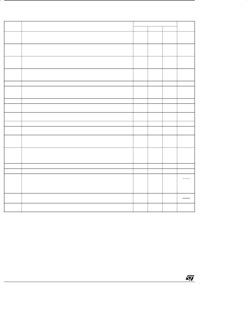
ELECTRICAL CHARACTERISTICS
LF355, LF356, LF357 |
0oC ≤ Tamb ≤ +70oC |
VCC = ±15V, (unless otherwise specified) |
||||||
Symbol |
|
|
Parameter |
|
LF355 - LF356 - LF357 |
Unit |
||
|
|
|
Min. |
Typ. |
Max. |
|||
|
|
|
|
|
|
|||
Vio |
Input Offset Voltage (RS = 50Ω) |
|
|
|
|
mV |
||
|
Tamb |
= 25oC |
≤ Tmax. |
|
|
3 |
10 |
|
|
Tmin. |
≤ Tamb |
|
|
|
13 |
|
|
Iio |
Input Offset Current - (note 3) |
|
|
|
|
|
||
|
Tamb |
= 25oC |
|
|
|
3 |
50 |
pA |
|
Tmin. |
≤ Tamb |
≤ Tmax. |
|
|
|
2 |
nA |
Iib |
Input Bias Current - (note 3) |
|
|
|
|
|
||
|
Tamb |
= 25oC |
|
|
|
20 |
200 |
pA |
|
Tmin. |
≤ Tamb |
≤ Tmax. |
|
|
|
8 |
nA |
Avd |
Large Signal Voltage Gain (RL = 2kΩ, VO = ±10V) |
|
|
|
V/mV |
|||
|
Tamb |
= 25oC |
|
|
25 |
200 |
|
|
|
Tmin. |
≤ Tamb |
≤ Tmax. |
|
15 |
|
|
|
SVR |
Supply Voltage Rejection Ratio - (note 4) |
|
80 |
100 |
|
dB |
||
ICC |
Supply Current (no load) |
|
|
|
|
mA |
||
|
Tamb = 25oC |
|
LF355 |
|
2 |
4 |
|
|
|
|
|
|
LF356, LF357 |
|
5 |
10 |
|
DVio |
Input Offset Voltage Drift (RS = 50Ω) - (note 2) |
|
5 |
|
μV/oC |
|||
DVio/Vio Change in Average Temperature Coefficient with Vio adjust |
|
0.5 |
|
μV/oC |
||||
|
(RS = 50Ω) |
|
|
|
|
|
per mV |
|
Vicm |
Input Common Mode Voltage Range (Tamb = 25oC) |
±10 |
+15.1 |
|
V |
|||
|
|
|
|
|
|
-12 |
|
|
CMR |
Common Mode Rejection Ratio |
|
80 |
100 |
|
dB |
||
±VOPP |
Output Voltage Swing |
RL = 10kΩ |
±12 |
±13 |
|
V |
||
|
|
|
|
RL = 2kΩ |
±10 |
±12 |
|
|
GBP |
Gain Bandwidth Product Tamb = 25oC) |
LF355 |
|
2.5 |
|
MHz |
||
|
|
|
|
LF356 |
|
5 |
|
|
|
|
|
|
LF357 |
|
20 |
|
|
SR |
Slew Rate (Tamb = 25oC) |
|
|
|
|
V/μs |
||
|
AV = 1 |
|
LF355 |
|
5 |
|
|
|
|
|
|
|
LF356 |
|
12 |
|
|
|
AV = 5 |
|
LF357 |
|
50 |
|
|
|
Ri |
Input Resistance (Tamb = 25oC) |
|
|
1012 |
|
Ω |
||
Ci |
Input Capacitance (Tamb = 25oC) |
|
|
3 |
|
pF |
||
en |
Equivalent Input Noise Voltage (Tamb = 25oC, RS = 100Ω) |
|
|
|
nV |
|||
|
f = 1000Hz |
|
LF355 |
|
20 |
|
```√ Hz |
|
|
|
|
|
LF356, LF357 |
|
12 |
|
|
|
f = 100Hz |
|
LF355 |
|
25 |
|
|
|
|
|
|
|
LF356, LF357 |
|
15 |
|
|
in |
EquivalentoInput Noise Current |
|
|
0.01 |
|
pA |
||
|
(Tamb = 25 C, f = 100Hz or f = 1000Hz) |
|
|
|
|
```√ Hz |
||
ts |
Settling Time (Tamb = 25oC) - (note 5) |
LF355 |
|
4 |
|
μs |
||
|
|
|
|
LF356, LF357 |
|
1.5 |
|
|
Notes : 1. Unless otherwise specified the absolute maximum negative input voltage is equal to the negative power supply voltage.
2.The temperature coefficient of the adjusted input offset voltage changes only a small amount (0.5μV/oC typically) for each mV of adjustment from its original unadjusted value. Common-mode rejection and open loop voltage gain are alsounaffected by offset adjustment.
3.The input bias currents are junction leakage currents which approximately double for every 10oC increase in the junction temperature Tamb. Due to limited production test time, the input bias current measured is correlated to junction temperature. In a normal operation the junction temperature rises above the ambient temperature as a result of internal power dissipation,
Ptot-Tamb =Tamb +Rth(j-a)xPtot where Rth(j-a) is the thermal resistance from junction to ambient. Use of a heatsink is recommended
f input currents are to be kept to a minimum.
4.Supply voltage rejection is measured for both supply magnitudes increasing or decreasing simultaneously, in accordance with common practise.
5.Settling time is defined here, for a unity gain inverter connection using 2kΩ resistors for the LF155, LF156 series. It is the time
required for the error voltage (the voltage at the inverting input pin on the amplifier) to settle to within 0.01% of its final value from the time a 10V step input is applied to the inverter. For the LF157 series AV = -5, the feedback resistor from output to input is 2kΩ and the output step is 10V.
4/14

APPLICATION HINTS
The LF155, LF156, LF157 series are op amps with J- FETinput transistors. TheseJFETs havelarge reverse breakdown voltagesfromgatetosource or drain eliminatingtheneed of clamps acrossthe inputs.Therefore large differential input voltages can easily be accommodatedwithoutalarge increaseof inputcurrents. The maximum differential input voltage is independent of the supplyvoltage. However, neitherof thenegativeinput voltagesshouldbe allowed to exceedthe negative supply as this will cause large currents to flow which can result in a destroyed unit. Exceeding the negative common-modelimit on either inputwill causeareversal of thephasetotheoutputandforce the amplifier output to the correspondinghigh or lowstate. Exceedingthe negativecommon-mode limit on bothinputs will force the amplifier outputto a highstate.In neithercasedoes a latch occur since raising the input back within the common-mode range again puts the input stage and thustheamplifierin a normal operatingmode. Exceedingthepositive common-modelimit on asingle input will not changethephase of the output however, if bothinputsexceedthe limit, theoutput of theamplifier will be forcedto ahighstate.Theseamplifierswill operatewith the common-mode input voltage equal to the positive supply. In fact, the common-modevoltagecanex- ceedthepositivesupplyby approximately100mV independentof supply volt-age and over thefull operatingtemperaturerange.The positive suplly can thereforebe used asa referenceonaninput as, forexample, in a supply current monitor and/orlimiter. Precautionsshouldbe taken to ensurethat thepowersupplyforthe integrated circuit never becomes re-versed in polarity or that the unit is not inadvertentlyin-stalledbackwards
LF155 - LF156 - LF157
in a socket as an unilimited current surge throughthe resulting forward diode within the IC couldcausefusingoftheinternalconductorsandresultin a destroyedunit. Because these amplifiers are JFET rather than MOSFET input op amps they do not require special handling.
Allof thebiascurrentsintheseamplifiersareset byFET current sources. The drain currents for the amplifiers are therefore essentially independent of supply voltages.
As with most amplifiers, care should betakenwith lead dress, components placement and supply decoupling in order to ensure stability. For example, resistors from the output to an input should be placed with the body close to theinput to minimiz ºpickupºand maximize the frequencyof the feedbackpole by minimizing the capacitancefromthe input to ground.
A feedback pole is createdwhen the feedbackaround any amplifier is resistive. The parallel resistance and capacitancefromthe input of thedevice(usuallythe invertinginput)toacgroundsetthefrequencyofthepole.In many instances the frequency of this pole is much greaterthanthe expected3 dBfrequencyof the closed loopgain and consequentlythereisnegligible effect on stability margin. However, if the feedback pole is less than approximately six time the expected 3 dB frequencyaleadcapacitor should be placed from the output to the input of the op amp. The value of that added capacitor should be such that the RC time constant of this capacitor and the resistance it parallels is greater than or equal to the original feedback pole time constant.
5/14
 Loading...