


CLC415MDC
NSC CLC415MDC, CLC415AMC, CLC415AJP, CLC415AJE-TR13, CLC415AJE Datasheet
...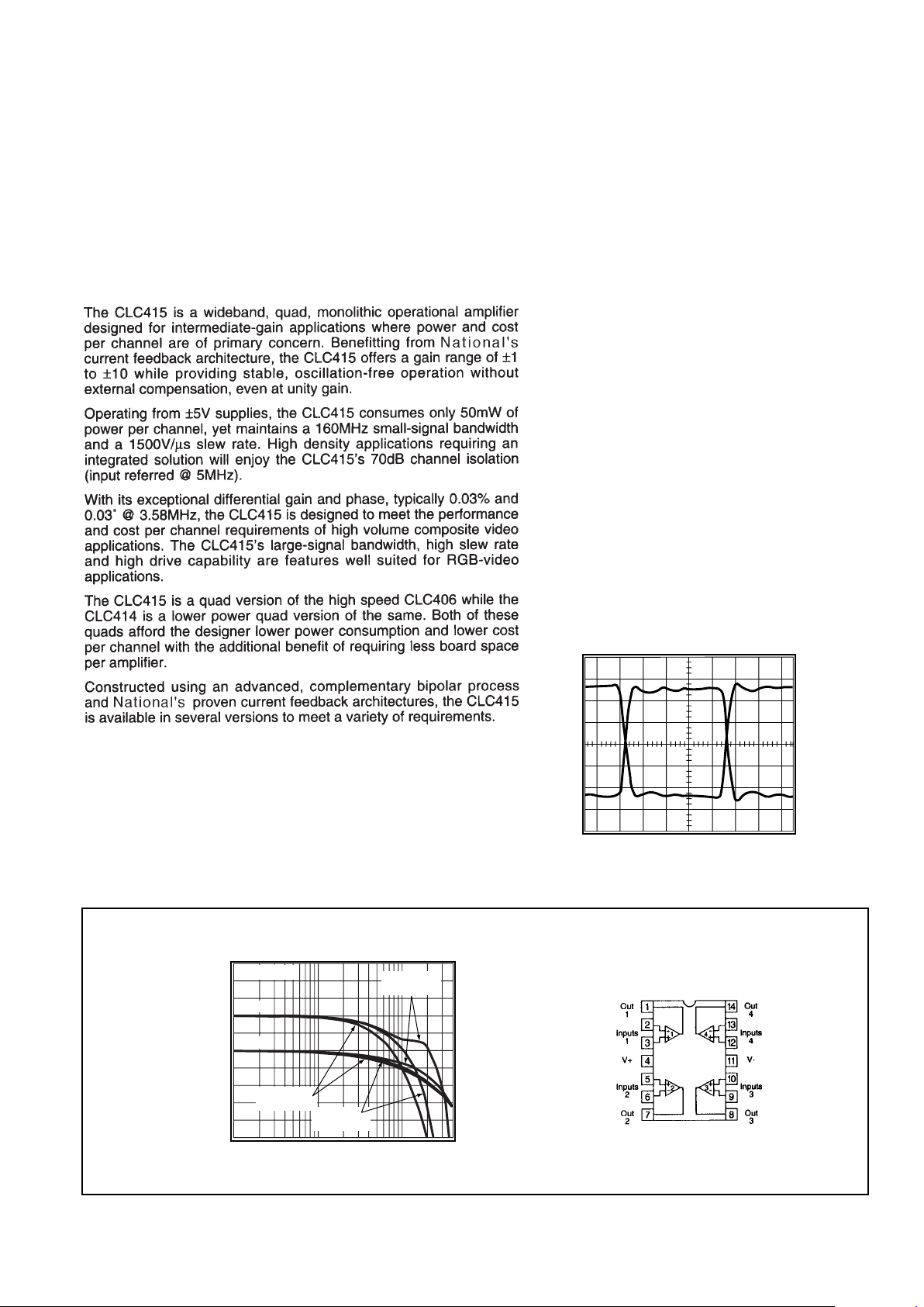
Small Signal Pulse Response
5ns/div
Output Voltage
A =+6
v
V = 2Vpp
o
+1.2
+0.8
+0.4
0
-0.4
-0.8
-1.2
A =-5
v
Features
■
160MHz small signal bandwidth
■
5mA quiescent current per amplifier
■
70dB channel isolation @ 5MHz
■
0.03%/0.03° differential gain/phase
■
12ns settling to 0.1%
■
1500V/µs slew rate
■
2.0ns rise and fall time (2Vpp)
■
70mA output current per amplifier
Applications
■
Composite video distribution amps
■
HDTV amplifiers
■
RGB-video amplifiers
■
CCD signal processing
■
Active Filters
■
Instrumentation differential amps
■
Channelized EW
General Description
CLC415
Quad,Wideband Monolithic Op Amp
N
June 1999
CLC415
Quad,Wideband Monolithic Op Amp
Non-Inverting Frequency Response
Magnitude (1dB/div)
1 Frequency (MHz) 100
Phase
0
-90
°
-180
°
-270
°
-360
°
-450
°
Vo = 2V
pp
Av = 6
Rf = 499Ω
A
v
= 2
Rf = 698Ω
A
v
= 10
Rf = 200Ω
Gain
Phase
Pinout
DIP & SOIC
© 1999 National Semiconductor Corporation http://www.national.com
Printed in the U.S.A.
CLC415AJP -40°C to +85°C 14-pin plastic DIP
CLC415AJE -40°C to +85°C 14-pin plastic SOIC
DESC SMD number: 5962-90994
CLC415 Electrical Characteristics
(Av= +6,Vcc= ±5V, RL= 100Ω,Rf= 500Ω; unless specified)
2
Absolute Maximum Ratings Miscellaneous Ratings
http://www.national.com 2
Min/max ratings are based on product characterization and simulation. Individual parameters are tested as noted. Outgoing quality levels are
determined from tested parameters.
Pac kage Thermal Resistance
Package θ
JC
θ
JA
AJP 55°C/W 105°C/W
AJE 45°C/W 115°C/W
CERDIP 30°C/W 80°C/W
Reliability Information
Transistor count 144
 Loading...