


 Loading...
Motorola MC68EC020FG16, MC68EC020FG25, MC68EC020RP16, MC68EC020RP25, MC68020RP16 Datasheet
...MC68020
MC68EC020
MICROPROCESSORS
USER’S MANUAL
First Edition
Motorola reserves the right to make changes without further notice to any products herein to improve reliability, function or design. Motorola does not assume any liability arising out of the application or use of any product or circuit described herein; neither does it convey any license under its patent rights nor the rights of others. Motorola products are not designed, intended, or authorized for use as components in systems intended for surgical implant into the body, or other applications intended to support or sustain life, or for any other application in which the failure of the Motorola product could create a situation where personal injury or death may occur. Should Buyer purchase or use Motorola products for any such unintended or unauthorized application, Buyer shall indemnify and hold Motorola and its officers, employees, subsidiaries, affiliates, and distributors harmless against all claims, costs, damages, and expenses, and reasonable attorney fees arising out of, directly or indirectly, any claim of personal injury or death associated with such unintended or unauthorized use, even if such claim alleges that Motorola was negligent regarding the design or manufacture of the part. Motorola and the  are registered trademarks of Motorola, Inc. Motorola, Inc. is an Equal Opportunity/Affirmative Action Employer.
© MOTOROLA INC., 1992
PREFACE
The M68020 User’s Manual describes the capabilities, operation, and programming of the
MC68020 32-bit, second-generation, enhanced microprocessor and the MC68EC020 32bit, second-generation, enhanced embedded microprocessor.
Throughout this manual, “MC68020/EC020” is used when information applies to both the
MC68020 and the MC68EC020. “MC68020” and “MC68EC020” are used when information applies only to the MC68020 or MC68EC020, respectively.
For detailed information on the MC68020 and MC68EC020 instruction set, refer to M68000PM/AD, M68000 Family Programmer’s Reference Manual.
This manual consists of the following sections:
Section 1 |
Introduction |
Section 2 |
Processing States |
Section 3 |
Signal Description |
Section 4 |
On-Chip Cache Memory |
Section 5 |
Bus Operation |
Section 6 |
Exception Processing |
Section 7 |
Coprocessor Interface Description |
Section 8 |
Instruction Execution Timing |
Section 9 |
Applications Information |
Section 10 |
Electrical Characteristics |
Section 11 Ordering Information and Mechanical Data |
|
Appendix A |
Interfacing an MC68EC020 to a DMA Device That Supports a Three-Wire |
|
Bus Arbitration Protocol |
NOTE
In this manual, assert and negate are used to specify forcing a signal to a particular state. In particular, assertion and assert refer to a signal that is active or true; negation and negate indicate a signal that is inactive or false. These terms are used independently of the voltage level (high or low) that they represent.
MOTOROLA |
M68020 USER’S MANUAL |
iii |
9/29/95 |
SECTION 1: OVERVIEW |
UM Rev 1 |
TABLE OF CONTENTS
Paragraph |
|
Page |
Number |
Title |
Number |
|
Section 1 |
|
|
Introduction |
|
1.1 |
Features .................................................................................................. |
1-2 |
1.2 |
Programming Model ................................................................................ |
1-4 |
1.3 |
Data Types and Addressing Modes Overview ........................................ |
1-8 |
1.4 |
Instruction Set Overview ......................................................................... |
1-10 |
1.5 |
Virtual Memory and Virtual Machine Concepts ....................................... |
1-10 |
1.5.1 |
Virtual Memory .................................................................................... |
1-10 |
1.5.2 |
Virtual Machine .................................................................................... |
1-12 |
1.6 |
Pipelined Architecture ............................................................................. |
1-12 |
1.7 |
Cache Memory ........................................................................................ |
1-13 |
|
Section 2 |
|
|
Processing States |
|
2.1 |
Privilege Levels ....................................................................................... |
2-2 |
2.1.1 |
Supervisor Privilege Level ................................................................... |
2-2 |
2.1.2 |
User Privilege Level ............................................................................. |
2-3 |
2.1.3 |
Changing Privilege Level ..................................................................... |
2-3 |
2.2 |
Address Space Types ............................................................................. |
2-4 |
2.3 |
Exception Processing.............................................................................. |
2-5 |
2.3.1 |
Exception Vectors ................................................................................ |
2-5 |
2.3.2 |
Exception Stack Frame ....................................................................... |
2-6 |
|
Section 3 |
|
|
Signal Description |
|
3.1 |
Signal Index ............................................................................................ |
3-2 |
3.2 |
Function Code Signals (FC2–FC0) ......................................................... |
3-2 |
3.3 |
Address Bus (A31–A0, MC68020)(A23–A0, MC68EC020) .................... |
3-2 |
3.4 |
Data Bus (D31–D0) ................................................................................. |
3-2 |
3.5 |
Transfer Size Signals (SIZ1, SIZ0) ......................................................... |
3-2 |
3.6 |
Asynchronous Bus Control Signals ......................................................... |
3-4 |
3.7 |
Interrupt Control Signals.......................................................................... |
3-5 |
3.8 |
Bus Arbitration Control Signals ............................................................... |
3-6 |
3.9 |
Bus Exception Control Signals ................................................................ |
3-6 |
3.10 |
Emulator Support Signal ......................................................................... |
3-7 |
3.11 |
Clock (CLK) ............................................................................................. |
3-7 |
MOTOROLA |
M68020 USER’S MANUAL |
vii |
9/29/95 SECTION 1: OVERVIEW UM Rev.1.0
TABLE OF CONTENTS (Continued)
Paragraph |
|
Page |
Number |
Title |
Number |
3.12 |
Power Supply Connections ..................................................................... |
3-7 |
3.13 |
Signal Summary...................................................................................... |
3-8 |
|
Section 4 |
|
|
On-Chip Cache Memory |
|
4.1 |
On-Chip Cache Organization and Operation .......................................... |
4-1 |
4.2 |
Cache Reset ........................................................................................... |
4-3 |
4.3 |
Cache Control ......................................................................................... |
4-3 |
4.3.1 |
Cache Control Register (CACR) ......................................................... |
4-3 |
4.3.2 |
Cache Address Register (CAAR) ........................................................ |
4-4 |
|
Section 5 |
|
|
Bus Operation |
|
5.1 |
Bus Transfer Signals............................................................................... |
5-1 |
5.1.1 |
Bus Control Signals ............................................................................. |
5-2 |
5.1.2 |
Address Bus ........................................................................................ |
5-3 |
5.1.3 |
Address Strobe .................................................................................... |
5-3 |
5.1.4 |
Data Bus.............................................................................................. |
5-3 |
5.1.5 |
Data Strobe ......................................................................................... |
5-4 |
5.1.6 |
Data Buffer Enable .............................................................................. |
5-4 |
5.1.7 |
Bus Cycle Termination Signals............................................................ |
5-4 |
5.2 |
Data Transfer Mechanism....................................................................... |
5-5 |
5.2.1 |
Dynamic Bus Sizing ............................................................................ |
5-5 |
5.2.2 |
Misaligned Operands........................................................................... |
5-14 |
5.2.3 |
Effects of Dynamic Bus Sizing and Operand Misalignment ................ |
5-20 |
5.2.4 |
Address, Size, and Data Bus Relationships ........................................ |
5-21 |
5.2.5 |
Cache Interactions .............................................................................. |
5-22 |
5.2.6 |
Bus Operation ..................................................................................... |
5-24 |
5.2.7 |
Synchronous Operation with DSACK1/DSACK0 ............................... |
5-24 |
5.3 |
Data Transfer Cycles .............................................................................. |
5-25 |
5.3.1 |
Read Cycle .......................................................................................... |
5-26 |
5.3.2 |
Write Cycle .......................................................................................... |
5-33 |
5.3.3 |
Read-Modify-Write Cycle..................................................................... |
5-39 |
5.4 |
CPU Space Cycles ................................................................................. |
5-44 |
5.4.1 |
Interrupt Acknowledge Bus Cycles ...................................................... |
5-45 |
5.4.1.1 |
Interrupt Acknowledge Cycle—Terminated Normally ...................... |
5-45 |
5.4.1.2 |
Autovector Interrupt Acknowledge Cycle ......................................... |
5-48 |
5.4.1.3 |
Spurious Interrupt Cycle .................................................................. |
5-48 |
5.4.2 |
Breakpoint Acknowledge Cycle ........................................................... |
5-50 |
5.4.3 |
Coprocessor Communication Cycles .................................................. |
5-53 |
5.5 |
Bus Exception Control Cycles................................................................. |
5-53 |
5.5.1 |
Bus Errors ........................................................................................... |
5-55 |
viii |
M68020 USER’S MANUAL |
MOTOROLA |
9/29/95 SECTION 1: OVERVIEW UM Rev 1
TABLE OF CONTENTS (Continued)
Paragraph |
|
Page |
Number |
Title |
Number |
5.5.2 |
Retry Operation ................................................................................... |
5-56 |
5.5.3 |
Halt Operation...................................................................................... |
5-60 |
5.5.4 |
Double Bus Fault ................................................................................. |
5-60 |
5.6 |
Bus Synchronization................................................................................ |
5-62 |
5.7 |
Bus Arbitration ......................................................................................... |
5-62 |
5.7.1 |
MC68020 Bus Arbitration .................................................................... |
5-63 |
5.7.1.1 |
Bus Request (MC68020) ................................................................. |
5-66 |
5.7.1.2 |
Bus Grant (MC68020) ...................................................................... |
5-66 |
5.7.1.3 |
Bus Grant Acknowledge (MC68020) ............................................... |
5-66 |
5.7.1.4 |
Bus Arbitration Control (MC68020) .................................................. |
5-67 |
5.7.2 |
MC68EC020 Bus Arbitration ............................................................... |
5-70 |
5.7.2.1 |
Bus Request (MC68EC020) ............................................................ |
5-71 |
5.7.2.2 |
Bus Grant (MC68EC020) ................................................................. |
5-71 |
5.7.2.3 |
Bus Arbitration Control (MC68EC020) ............................................. |
5-73 |
5.8 |
Reset Operation ...................................................................................... |
5-76 |
Section 6
Exception Processing
6.1 |
Exception Processing Sequence ............................................................ |
6-1 |
6.1.1 |
Reset Exception................................................................................... |
6-4 |
6.1.2 |
Bus Error Exception ............................................................................. |
6-4 |
6.1.3 |
Address Error Exception...................................................................... |
6-6 |
6.1.4 |
Instruction Trap Exception ................................................................... |
6-6 |
6.1.5 |
Illegal Instruction and Unimplemented Instruction Exceptions ............ |
6-7 |
6.1.6 |
Privilege Violation Exception ............................................................... |
6-8 |
6.1.7 |
Trace Exception ................................................................................... |
6-9 |
6.1.8 |
Format Error Exception ....................................................................... |
6-10 |
6.1.9 |
Interrupt Exceptions ............................................................................. |
6-11 |
6.1.10 |
Breakpoint Instruction Exception ......................................................... |
6-17 |
6.1.11 |
Multiple Exceptions.............................................................................. |
6-17 |
6.1.12 |
Return from Exception ......................................................................... |
6-19 |
6.2 |
Bus Fault Recovery ................................................................................. |
6-21 |
6.2.1 |
Special Status Word (SSW)................................................................. |
6-21 |
6.2.2 |
Using Software to Complete the Bus Cycles ....................................... |
6-23 |
6.2.3 |
Completing the Bus Cycles with RTE .................................................. |
6-24 |
6.3 |
Coprocessor Considerations ................................................................... |
6-25 |
6.4 |
Exception Stack Frame Formats ............................................................. |
6-25 |
MOTOROLA |
M68020 USER’S MANUAL |
ix |
9/29/95 SECTION 1: OVERVIEW UM Rev.1.0
TABLE OF CONTENTS (Continued)
Paragraph |
|
Page |
Number |
Title |
Number |
|
Section 7 |
|
|
Coprocessor Interface Description |
|
7.1 |
Introduction ............................................................................................. |
7-1 |
7.1.1 |
Interface Features ............................................................................... |
7-2 |
7.1.2 |
Concurrent Operation Support ............................................................ |
7-2 |
7.1.3 |
Coprocessor Instruction Format .......................................................... |
7-3 |
7.1.4 |
Coprocessor System Interface ............................................................ |
7-4 |
7.1.4.1 |
Coprocessor Classification .............................................................. |
7-4 |
7.1.4.2 |
Processor-Coprocessor Interface .................................................... |
7-5 |
7.1.4.3 |
Coprocessor Interface Register Selection ....................................... |
7-6 |
7.2 |
Coprocessor Instruction Types ............................................................... |
7-7 |
7.2.1 |
Coprocessor General Instructions ....................................................... |
7-8 |
7.2.1.1 |
Format ............................................................................................. |
7-8 |
7.2.1.2 |
Protocol............................................................................................ |
7-9 |
7.2.2 |
Coprocessor Conditional Instructions.................................................. |
7-10 |
7.2.2.1 |
Branch on Coprocessor Condition Instruction ................................. |
7-12 |
7.2.2.1.1 |
Format .......................................................................................... |
7-12 |
7.2.2.1.2 |
Protocol ........................................................................................ |
7-12 |
7.2.2.2 |
Set on Coprocessor Condition Instruction ....................................... |
7-13 |
7.2.2.2.1 |
Format .......................................................................................... |
7-13 |
7.2.2.2.2 |
Protocol ........................................................................................ |
7-14 |
7.2.2.3 |
Test Coprocessor Condition, Decrement, and Branch Instruction ...7-14 |
|
7.2.2.3.1 |
Format .......................................................................................... |
7-14 |
7.2.2.3.2 |
Protocol ........................................................................................ |
7-15 |
7.2.2.4 |
Trap on Coprocessor Condition Instruction ..................................... |
7-15 |
7.2.2.4.1 |
Format .......................................................................................... |
7-15 |
7.2.2.4.2 |
Protocol ........................................................................................ |
7-16 |
7.2.3 |
Coprocessor Context Save and Restore Instructions ......................... |
7-16 |
7.2.3.1 |
Coprocessor Internal State Frames ................................................. |
7-17 |
7.2.3.2 |
Coprocessor Format Words............................................................. |
7-18 |
7.2.3.2.1 |
Empty/Reset Format Word ........................................................... |
7-18 |
7.2.3.2.2 |
Not-Ready Format Word .............................................................. |
7-19 |
7.2.3.2.3 |
Invalid Format Word ..................................................................... |
7-19 |
7.2.3.2.4 |
Valid Format Word ....................................................................... |
7-20 |
7.2.3.3 |
Coprocessor Context Save Instruction ............................................ |
7-20 |
7.2.3.3.1 |
Format .......................................................................................... |
7-20 |
7.2.3.3.2 |
Protocol ........................................................................................ |
7-21 |
7.2.3.4 |
Coprocessor Context Restore Instruction ........................................ |
7-22 |
7.2.3.4.1 |
Format .......................................................................................... |
7-22 |
7.2.3.4.2 |
Protocol ........................................................................................ |
7-23 |
7.3 |
Coprocessor Interface Register Set ........................................................ |
7-24 |
x |
M68020 USER’S MANUAL |
MOTOROLA |
9/29/95 SECTION 1: OVERVIEW UM Rev 1
TABLE OF CONTENTS (Continued)
Paragraph |
|
Page |
Number |
Title |
Number |
7.3.1 |
Response CIR ..................................................................................... |
7-24 |
7.3.2 |
Control CIR .......................................................................................... |
7-24 |
7.3.3 |
Save CIR ............................................................................................. |
7-25 |
7.3.4 |
Restore CIR ......................................................................................... |
7-25 |
7.3.5 |
Operation Word CIR ............................................................................ |
7-25 |
7.3.6 |
Command CIR ..................................................................................... |
7-25 |
7.3.7 |
Condition CIR ...................................................................................... |
7-26 |
7.3.8 |
Operand CIR ....................................................................................... |
7-26 |
7.3.9 |
Register Select CIR ............................................................................. |
7-27 |
7.3.10 |
Instruction Address CIR ....................................................................... |
7-27 |
7.3.11 |
Operand Address CIR ......................................................................... |
7-27 |
7.4 |
Coprocessor Response Primitives .......................................................... |
7-27 |
7.4.1 |
ScanPC ............................................................................................... |
7-28 |
7.4.2 |
Coprocessor Response Primitive General Format .............................. |
7-28 |
7.4.3 |
Busy Primitive ...................................................................................... |
7-30 |
7.4.4 |
Null Primitive ........................................................................................ |
7-31 |
7.4.5 |
Supervisor Check Primitive ................................................................. |
7-33 |
7.4.6 |
Transfer Operation Word Primitive ...................................................... |
7-33 |
7.4.7 |
Transfer from Instruction Stream Primitive .......................................... |
7-34 |
7.4.8 |
Evaluate and Transfer Effective Address Primitive ............................. |
7-35 |
7.4.9 |
Evaluate Effective Address and Transfer Data Primitive ..................... |
7-35 |
7.4.10 |
Write to Previously Evaluated Effective Address Primitive .................. |
7-37 |
7.4.11 |
Take Address and Transfer Data Primitive.......................................... |
7-39 |
7.4.12 |
Transfer to/from Top of Stack Primitive ............................................... |
7-40 |
7.4.13 |
Transfer Single Main Processor Register Primitive ............................. |
7-40 |
7.4.14 |
Transfer Main Processor Control Register Primitive ........................... |
7-41 |
7.4.15 |
Transfer Multiple Main Processor Registers Primitive ......................... |
7-42 |
7.4.16 |
Transfer Multiple Coprocessor Registers Primitive ............................. |
7-42 |
7.4.17 |
Transfer Status Register and ScanPC Primitive.................................. |
7-44 |
7.4.18 |
Take Preinstruction Exception Primitive .............................................. |
7-45 |
7.4.19 |
Take Midinstruction Exception Primitive .............................................. |
7-47 |
7.4.20 |
Take Postinstruction Exception Primitive ............................................ |
7-48 |
7.5 |
Exceptions ............................................................................................... |
7-49 |
7.5.1 |
Coprocessor-Detected Exceptions ...................................................... |
7-49 |
7.5.1.1 |
Coprocessor-Detected Protocol Violations ...................................... |
7-50 |
7.5.1.2 |
Coprocessor-Detected Illegal Command or Condition Words ......... |
7-51 |
7.5.1.3 |
Coprocessor Data-Processing-Related Exceptions ......................... |
7-51 |
7.5.1.4 |
Coprocessor System-Related Exceptions ....................................... |
7-51 |
7.5.1.5 |
Format Errors ................................................................................... |
7-52 |
7.5.2 |
Main-Processor-Detected Exceptions ................................................. |
7-52 |
7.5.2.1 |
Protocol Violations ........................................................................... |
7-52 |
7.5.2.2 |
F-Line Emulator Exceptions ............................................................. |
7-54 |
MOTOROLA |
M68020 USER’S MANUAL |
xi |
9/29/95 SECTION 1: OVERVIEW UM Rev.1.0
TABLE OF CONTENTS (Continued)
Paragraph |
|
Page |
Number |
Title |
Number |
7.5.2.3 |
Privilege Violations........................................................................... |
7-55 |
7.5.2.4 |
cpTRAPcc Instruction Traps ............................................................ |
7-55 |
7.5.2.5 |
Trace Exceptions ............................................................................. |
7-55 |
7.5.2.6 |
Interrupts .......................................................................................... |
7-56 |
7.5.2.7 |
Format Errors ................................................................................... |
7-57 |
7.5.2.8 |
Address and Bus Errors................................................................... |
7-57 |
7.5.3 |
Coprocessor Reset .............................................................................. |
7-58 |
7.6 |
Coprocessor Summary ........................................................................... |
7-58 |
Section 8
Instruction Execution Timing
8.1 |
Timing Estimation Factors ...................................................................... |
8-1 |
8.1.1 |
Instruction Cache and Prefetch ........................................................... |
8-1 |
8.1.2 |
Operand Misalignment ........................................................................ |
8-2 |
8.1.3 |
Bus/Sequencer Concurrency............................................................... |
8-2 |
8.1.4 |
Instruction Execution Overlap ............................................................. |
8-3 |
8.1.5 |
Instruction Stream Timing Examples ................................................... |
8-4 |
8.2 |
Instruction Timing Tables ........................................................................ |
8-9 |
8.2.1 |
Fetch Effective Address ...................................................................... |
8-13 |
8.2.2 |
Fetch Immediate Effective Address..................................................... |
8-14 |
8.2.3 |
Calculate Effective Address ................................................................ |
8-16 |
8.2.4 |
Calculate Immediate Effective Address............................................... |
8-17 |
8.2.5 |
Jump Effective Address....................................................................... |
8-19 |
8.2.6 |
MOVE Instruction ................................................................................ |
8-20 |
8.2.7 |
Special-Purpose MOVE Instruction ..................................................... |
8-29 |
8.2.8 |
Arithmetic/Logical Instructions............................................................. |
8-30 |
8.2.9 |
Immediate Arithmetic/Logical Instructions ........................................... |
8-31 |
8.2.10 |
Binary-Coded Decimal Operations ...................................................... |
8-32 |
8.2.11 |
Single-Operand Instructions ................................................................ |
8-33 |
8.2.12 |
Shift/Rotate Instructions ...................................................................... |
8-34 |
8.2.13 |
Bit Manipulation Instructions ............................................................... |
8-35 |
8.2.14 |
Bit Field Manipulation Instructions....................................................... |
8-36 |
8.2.15 |
Conditional Branch Instructions........................................................... |
8-37 |
8.2.16 |
Control Instructions.............................................................................. |
8-38 |
8.2.17 |
Exception-Related Instructions ............................................................ |
8-39 |
8.2.18 |
Save and Restore Operations ............................................................. |
8-40 |
|
Section 9 |
|
|
Applications Information |
|
9.1 |
Floating-Point Units ................................................................................. |
9-1 |
9.2 |
Byte Select Logic for the MC68020/EC020............................................. |
9-5 |
9.3 |
Power and Ground Considerations ......................................................... |
9-9 |
xii |
M68020 USER’S MANUAL |
MOTOROLA |
9/29/95 SECTION 1: OVERVIEW UM Rev 1
TABLE OF CONTENTS (Concluded)
Paragraph |
|
Page |
Number |
Title |
Number |
9.4 |
Clock Driver............................................................................................. |
9-10 |
9.5 |
Memory Interface .................................................................................... |
9-11 |
9.6 |
Access Time Calculations ....................................................................... |
9-12 |
9.7 |
Module Support ....................................................................................... |
9-14 |
9.7.1 |
Module Descriptor................................................................................ |
9-14 |
9.7.2 |
Module Stack Frame ........................................................................... |
9-16 |
9.8 |
Access Levels ......................................................................................... |
9-17 |
9.8.1 |
Module Call.......................................................................................... |
9-18 |
9.8.2 |
Module Return ..................................................................................... |
9-19 |
|
Section 10 |
|
|
Electrical Characteristics |
|
10.1 |
Maximum Ratings ................................................................................. |
10-1 |
10.2 |
Thermal Considerations ........................................................................ |
10-1 |
10.2.1MC68020 Thermal Characteristics and
DC Electrical Characteristics ........................................................... |
10-2 |
10.2.2MC68EC020 Thermal Characteristics and
|
DC Electrical Characteristics ........................................................... |
10-4 |
10.3 |
AC Electrical Characteristics ................................................................. |
10-5 |
|
Section 11 |
|
|
Ordering Information and Mechanical Data |
|
11.1 |
Standard Ordering Information.............................................................. |
11-1 |
11.1.1 |
Standard MC68020 Ordering Information.......................................... |
11-1 |
11.1.2 |
Standard MC68EC020 Ordering Information .................................... |
11-1 |
11.2 |
Pin Assignments and Package Dimensions .......................................... |
11-2 |
11.2.1 |
MC68020 RC and RP Suffix—Pin Assignment ................................. |
11-2 |
11.2.2 |
MC68020 RC Suffix—Package Dimensions ................................ ..... |
11-3 |
11.2.3 |
MC68020 RP Suffix—Package Dimensions...................................... |
11-4 |
11.2.4 |
MC68020 FC and FE Suffix—Pin Assignment .................................. |
11-5 |
11.2.5 |
MC68020 FC Suffix—Package Dimensions ...................................... |
11-6 |
11.2.6 |
MC68020 FE Suffix—Package Dimensions ...................................... |
11-7 |
11.2.7 |
MC68EC020 RP Suffix—Pin Assignment.......................................... |
11-8 |
11.2.8 |
MC68EC020 RP Suffix—Package Dimensions ................................. |
11-9 |
11.2.9 |
MC68EC020 FG Suffix—Pin Assignment.......................................... |
11-10 |
11.2.10 |
MC68EC020 FG Suffix—Package Dimensions ................................. |
11-11 |
Appendix A
Interfacing an MC68EC020 to a DMA Device That
Supports a Three-Wire Bus Arbitration Protocol
MOTOROLA |
M68020 USER’S MANUAL |
xiii |
9/29/95 |
SECTION 1: OVERVIEW |
UM Rev.1.0 |
LIST OF ILLUSTRATIONS
Figure |
|
|
Page |
Number |
Title |
Number |
|
1-1 |
MC68020/EC020 Block Diagram ..................................................................... |
|
1-3 |
1-2 |
User Programming Model ................................................................................ |
|
1-5 |
1-3 |
Supervisor Programming Model Supplement .................................................. |
1-6 |
|
1-4 |
Status Register (SR) ........................................................................................ |
|
1-7 |
1-5 |
Instruction Pipe ................................................................................................ |
|
1-13 |
2-1 |
General Exception Stack Frame ...................................................................... |
|
2-6 |
3-1 |
Functional Signal Groups ................................................................................. |
|
3-1 |
4-1 |
MC68020/EC020 On-Chip Cache Organization .............................................. |
4-2 |
|
4-2 |
Cache Control Register .................................................................................... |
|
4-3 |
4-3 |
Cache Address Register .................................................................................. |
|
4-4 |
5-1 |
Relationship between External and Internal Signals........................................ |
5-2 |
|
5-2 |
Input Sample Window ...................................................................................... |
|
5-2 |
5-3 |
Internal Operand Representation ..................................................................... |
|
5-6 |
5-4 |
MC68020/EC020 Interface to Various Port Sizes ............................................ |
5-6 |
|
5-5 |
Long-Word Operand Write to Word Port Example........................................... |
5-10 |
|
5-6 |
Long-Word Operand Write to Word Port Timing .............................................. |
5-11 |
|
5-7 |
Word Operand Write to Byte Port Example ..................................................... |
5-12 |
|
5-8 |
Word Operand Write to Byte Port Timing......................................................... |
5-13 |
|
5-9 |
Misaligned Long-Word Operand Write to Word Port Example ........................ |
5-14 |
|
5-10 |
Misaligned Long-Word Operand Write to Word Port Timing............................ |
5-15 |
|
5-11 |
Misaligned Long-Word Operand Read from Word Port Example .................... |
5-16 |
|
5-12 |
Misaligned Word Operand Write to Word Port Example.................................. |
5-16 |
|
5-13 |
Misaligned Word Operand Write to Word Port Timing ..................................... |
5-17 |
|
5-14 |
Misaligned Word Operand Read from Word Bus Example .............................. |
5-18 |
|
5-15 |
Misaligned Long-Word Operand Write to Long-Word Port Example ............... |
5-18 |
|
5-16 |
Misaligned Long-Word Operand Write to Long-Word Port Timing .................. |
5-19 |
|
5-17 |
Misaligned Long-Word Operand Read from Long-Word Port Example ........... |
5-20 |
|
5-18 |
Byte Enable Signal Generation for 16and 32-Bit Ports.................................. |
5-23 |
|
5-19 |
Long-Word Read Cycle Flowchart ................................................................... |
|
5-26 |
5-20 |
Byte Read Cycle Flowchart .............................................................................. |
|
5-27 |
5-21 |
Byte and Word Read Cycles—32-Bit Port ....................................................... |
5-28 |
|
5-22 |
Long-Word Read—8-Bit Port ........................................................................... |
|
5-29 |
5-23 |
Long-Word Read—16- and 32-Bit Ports .......................................................... |
5-30 |
|
xiv |
M68020 USER’S MANUAL |
MOTOROLA |
9/29/95 SECTION 1: OVERVIEW UM Rev 1
LIST OF ILLUSTRATIONS (Continued)
Figure |
|
|
Page |
Number |
Title |
Number |
|
5-24 |
Write Cycle Flowchart ...................................................................................... |
|
5-33 |
5-25 |
Read-Write-Read Cycles—32-Bit Port ............................................................. |
5-34 |
|
5-26 |
Byte and Word Write Cycles—32-Bit Port ........................................................ |
5-35 |
|
5-27 |
Long-Word Operand Write—8-Bit Port ............................................................ |
5-36 |
|
5-28 |
Long-Word Operand Write—16-Bit Port........................................................... |
5-37 |
|
5-29 |
Read-Modify-Write Cycle Flowchart ................................................................. |
5-40 |
|
5-30 |
Byte Read-Modify-Write Cycle—32-Bit Port (TAS Instruction) ........................ |
5-41 |
|
5-31 |
MC68020/EC020 CPU Space Address Encoding ............................................ |
5-45 |
|
5-32 |
Interrupt Acknowledge Cycle Flowchart ........................................................... |
5-46 |
|
5-33 |
Interrupt Acknowledge Cycle Timing................................................................ |
5-47 |
|
5-34 |
Autovector Operation Timing ........................................................................... |
|
5-49 |
5-35 |
Breakpoint Acknowledge Cycle Flowchart ....................................................... |
5-50 |
|
5-36 |
Breakpoint Acknowledge Cycle Timing ............................................................ |
5-51 |
|
5-37 |
Breakpoint Acknowledge Cycle Timing (Exception Signaled) .......................... |
5-52 |
|
5-38 |
Bus Error without DSACK1/DSACK0 ............................................................. |
5-57 |
|
5-39 |
Late Bus Error with DSACK1/DSACK0 .......................................................... |
5-58 |
|
5-40 |
Late Retry......................................................................................................... |
|
5-59 |
5-41 |
Halt Operation Timing ...................................................................................... |
|
5-61 |
5-42 |
MC68020 Bus Arbitration Flowchart for Single Request .................................. |
5-64 |
|
5-43 |
MC68020 Bus Arbitration Operation Timing for Single Request ...................... |
5-65 |
|
5-44 |
MC68020 Bus Arbitration State Diagram ......................................................... |
5-67 |
|
5-45 |
MC68020 Bus Arbitration Operation Timing—Bus Inactive ............................. |
5-69 |
|
5-46 |
MC68EC020 Bus Arbitration Flowchart for Single Request ............................. |
5-71 |
|
5-47 |
MC68EC020 Bus Arbitration Operation Timing for Single Request ................. |
5-72 |
|
5-48 |
MC68EC020 Bus Arbitration State Diagram .................................................... |
5-73 |
|
5-49 |
MC68EC020 Bus Arbitration Operation Timing—Bus Inactive ........................ |
5-75 |
|
5-50 |
Interface for Three-Wire to Two-Wire Bus Arbitration ...................................... |
5-76 |
|
5-51 |
Initial Reset Operation Timing .......................................................................... |
|
5-77 |
5-52 |
RESET Instruction Timing ................................................................................ |
|
5-78 |
6-1 |
Reset Operation Flowchart .............................................................................. |
|
6-5 |
6-2 |
Interrupt Pending Procedure ............................................................................ |
|
6-12 |
6-3 |
Interrupt Recognition Examples ....................................................................... |
|
6-13 |
6-4 |
Assertion of IPEND (MC68020 Only) ............................................................... |
6-14 |
|
6-5 |
Interrupt Exception Processing Flowchart ........................................................ |
6-15 |
|
6-6 |
Breakpoint Instruction Flowchart ...................................................................... |
|
6-18 |
6-7 |
RTE Instruction for Throwaway Four-Word Frame .......................................... |
6-20 |
|
6-8 |
Special Status Word Format ............................................................................ |
|
6-22 |
7-1 |
F-Line Coprocessor Instruction Operation Word.............................................. |
7-3 |
|
7-2 |
Asynchronous Non-DMA M68000 Coprocessor Interface Signal Usage ......... |
7-5 |
|
7-3 |
MC68020/EC020 CPU Space Address Encodings .......................................... |
7-6 |
|
MOTOROLA |
M68020 USER’S MANUAL |
xv |
9/29/95 SECTION 1: OVERVIEW UM Rev.1.0
LIST OF ILLUSTRATIONS (Continued)
Figure |
|
|
Page |
Number |
Title |
Number |
|
7-4 |
Coprocessor Address Map in MC68020/EC020 CPU Space .......................... |
7-7 |
|
7-5 |
Coprocessor Interface Register Set Map ......................................................... |
7-7 |
|
7-6 |
Coprocessor General Instruction Format (cpGEN) .......................................... |
7-8 |
|
7-7 |
Coprocessor Interface Protocol for General Category Instructions.................. |
7-10 |
|
7-8 |
Coprocessor Interface Protocol for Conditional Category Instructions ............ |
7-11 |
|
7-9 |
Branch on Coprocessor Condition Instruction Format (cpBcc.W) ................... |
7-12 |
|
7-10 |
Branch on Coprocessor Condition Instruction Format (cpBcc.L) ..................... |
7-12 |
|
7-11 |
Set on Coprocessor Condition Instruction Format (cpScc) .............................. |
7-13 |
|
7-12 |
Test Coprocessor Condition, Decrement, and Branch |
|
|
|
Instruction Format (cpDBcc) |
........................................................................... |
7-14 |
7-13 |
Trap on Coprocessor Condition .....................Instruction Format (cpTRAPcc) |
7-15 |
|
7-14 |
Coprocessor State Frame Format ..................................................in Memory |
7-17 |
|
7-15 |
Coprocessor Context Save Instruction ...............................Format (cpSAVE) |
7-20 |
|
7-16 |
Coprocessor Context Save Instruction ..............................................Protocol |
7-21 |
|
7-17 |
Coprocessor Context Restore ...................Instruction Format (cpRESTORE) |
7-22 |
|
7-18 |
Coprocessor Context Restore ..........................................Instruction Protocol |
7-23 |
|
7-19 |
Control CIR Format .......................................................................................... |
|
7-25 |
7-20 |
Condition CIR Format ...................................................................................... |
|
7-26 |
7-21 |
Operand Alignment for Operand ..............................................CIR Accesses |
7-26 |
|
7-22 |
Coprocessor Response Primitive ........................................................Format |
7-28 |
|
7-23 |
Busy Primitive Format ...................................................................................... |
|
7-30 |
7-24 |
Null Primitive Format........................................................................................ |
|
7-31 |
7-25 |
Supervisor Check Primitive Format.................................................................. |
7-33 |
|
7-26 |
Transfer Operation Word Primitive ......................................................Format |
7-33 |
|
7-27 |
Transfer from Instruction Stream ..........................................Primitive Format |
7-34 |
|
7-28 |
Evaluate and Transfer Effective ..............................Address Primitive Format |
7-35 |
|
7-29 |
Evaluate Effective Address and .....................Transfer Data Primitive Format |
7-35 |
|
7-30 |
Write to Previously Evaluated ..................Effective Address Primitive Format |
7-37 |
|
7-31 |
Take Address and Transfer Data ..........................................Primitive Format |
7-39 |
|
7-32 |
Transfer to/from Top of Stack ...............................................Primitive Format |
7-40 |
|
7-33 |
Transfer Single Main Processor .............................Register Primitive Format |
7-40 |
|
7-34 |
Transfer Main Processor Control ...........................Register Primitive Format |
7-41 |
|
7-35 |
Transfer Multiple Main Processor .........................Registers Primitive Format |
7-42 |
|
7-36 |
Register Select Mask Format ........................................................................... |
|
7-42 |
7-37 |
Transfer Multiple Coprocessor ..............................Registers Primitive Format |
7-43 |
|
7-38 |
Operand Format in Memory for ...........................................Transfer to –(An) |
7-44 |
|
7-39 |
Transfer Status Register and ..................................ScanPC Primitive Format |
7-44 |
|
7-40 |
Take Preinstruction Exception ..............................................Primitive Format |
7-45 |
|
7-41 |
MC68020/EC020 Preinstruction .................................................Stack Frame |
7-46 |
|
7-42 |
Take Midinstruction Exception ..............................................Primitive Format |
7-47 |
|
7-43 |
MC68020/EC020 Midinstruction .................................................Stack Frame |
7-47 |
|
7-44 |
Take Postinstruction Exception .............................................Primitive Format |
7-48 |
|
xvi |
M68020 USER’S MANUAL |
MOTOROLA |
9/29/95 SECTION 1: OVERVIEW UM Rev 1
LIST OF ILLUSTRATIONS (Concluded)
Figure |
|
|
Page |
Number |
Title |
Number |
|
7-45 |
MC68020/EC020 Postinstruction Stack Frame................................................ |
7-48 |
|
8-1 |
Concurrent Instruction Execution |
..................................................................... |
8-3 |
8-2 |
Instruction Execution for Instruction .....................................Timing Purposes |
8-3 |
|
8-3 |
Processor Activity for Example 1 ..................................................................... |
|
8-5 |
8-4 |
Processor Activity for Example 2 ..................................................................... |
|
8-6 |
8-5 |
Processor Activity for Example 3 ..................................................................... |
|
8-7 |
8-6 |
Processor Activity for Example 4 ..................................................................... |
|
8-8 |
9-1 |
32-Bit Data Bus Coprocessor Connection........................................................ |
9-2 |
|
9-2 |
Chip Select Generation PAL ............................................................................ |
|
9-3 |
9-3 |
Chip Select PAL Equations .............................................................................. |
|
9-4 |
9-4 |
Bus Cycle Timing Diagram ............................................................................... |
|
9-4 |
9-5 |
Example MC68020/EC020 Byte Select ................PAL System Configuration |
9-7 |
|
9-6 |
MC68020/EC020 Byte Select PAL ..................................................Equations |
9-8 |
|
9-7 |
High-Resolution Clock Controller ..................................................................... |
|
9-11 |
9-8 |
Alternate Clock Solution ................................................................................... |
|
9-11 |
9-9 |
Access Time Computation Diagram ................................................................. |
9-12 |
|
9-10 |
Module Descriptor Format ................................................................................ |
|
9-15 |
9-11 |
Module Entry Word .......................................................................................... |
|
9-15 |
9-12 |
Module Call Stack Frame ................................................................................. |
|
9-16 |
9-13 |
Access Level Control Bus Registers ................................................................ |
9-17 |
|
10-1 |
Drive Levels and Test Points for AC .......................................Specifications |
10-6 |
|
10-2 |
Clock Input Timing Diagram ........................................................................... |
|
10-7 |
10-3 |
Read Cycle Timing Diagram .......................................................................... |
|
10-11 |
10-4 |
Write Cycle Timing Diagram........................................................................... |
|
10-12 |
10-5 |
Bus Arbitration Timing Diagram ..................................................................... |
|
10-13 |
A-1 |
Bus Arbitration Circuit—MC68EC020 .........(Two-Wire) to DMA (Three-Wire) |
A-1 |
|
MOTOROLA |
M68020 USER’S MANUAL |
xvii |
9/29/95 |
SECTION 1: OVERVIEW |
UM Rev.1.0 |
LIST OF TABLES
Table |
|
|
Page |
Number |
Title |
Number |
|
1-1 |
Addressing Modes ........................................................................................... |
|
1-9 |
1-2 |
Instruction Set .................................................................................................. |
|
1-11 |
2-1 |
Address Space Encodings ............................................................................... |
|
2-4 |
3-1 |
Signal Index ..................................................................................................... |
|
3-3 |
3-2 |
Signal Summary............................................................................................... |
|
3-8 |
5-1 |
DSACK1/DSACK0 Encodings and Results .................................................... |
5-5 |
|
5-2 |
SIZ1, SIZ0 Signal Encoding ............................................................................. |
|
5-7 |
5-3 |
Address Offset Encodings ............................................................................... |
|
5-7 |
5-4 |
Data Bus Requirements for Read Cycles ........................................................ |
5-8 |
|
5-5 |
MC68020/EC020 Internal to External Data Bus Multiplexer— |
|
|
|
Write Cycles ................................................................................................... |
|
5-9 |
5-6 |
Memory Alignment and Port Size Influence on Read/Write Bus Cycles .......... |
5-20 |
|
5-7 |
Data Bus Byte Enable Signals for Byte, Word, and Long-Word Ports ............. |
5-22 |
|
5-8 |
DSACK1/DSACK0, BERR, HALT Assertion Results ..................................... |
5-54 |
|
6-1 |
Exception Vector Assignments ........................................................................ |
|
6-3 |
6-2 |
Tracing Control ................................................................................................ |
|
6-9 |
6-3 |
Interrupt Levels and Mask Values.................................................................... |
|
6-12 |
6-4 |
Exception Priority Groups ................................................................................ |
|
6-18 |
6-5 |
Exception Stack Frames .................................................................................. |
|
6-26 |
7-1 |
cpTRAPcc Opmode Encodings........................................................................ |
|
7-16 |
7-2 |
Coprocessor Format Word Encodings ............................................................. |
7-18 |
|
7-3 |
Null Coprocessor Response Primitive Encodings............................................ |
7-32 |
|
7-4 |
Valid Effective Address Field Codes ................................................................ |
7-36 |
|
7-5 |
Main Processor Control Register Select Codes............................................... |
7-41 |
|
7-6 |
Exceptions Related to Primitive Processing .................................................... |
7-53 |
|
8-1 |
Examples 1–4 Instruction Stream Execution Comparison ............................... |
8-8 |
|
8-2 |
Instruction Timings from Timing Tables ........................................................... |
8-11 |
|
8-3 |
Observed Instruction Timings .......................................................................... |
|
8-11 |
xviii |
M68020 USER’S MANUAL |
MOTOROLA |
9/29/95 SECTION 1: OVERVIEW UM Rev 1
LIST OF TABLES (Continued)
Table |
|
|
Page |
Number |
Title |
Number |
|
9-1 |
Data Bus Activity for Byte, Word, and Long-Word Ports .................................. |
9-6 |
|
9-2 |
VCC and GND Pin Assignments—MC68EC020 PPGA (RP Suffix) ................. |
9-10 |
|
9-3 |
VCC and GND Pin Assignments—MC68EC020 PQFP (FG Sufffix)................. |
9-10 |
|
9-4 |
Memory Access Time Equations at 16.67 and 25 MHz ................................... |
9-13 |
|
9-5 |
Calculated tAVDV Values for Operation at Frequencies |
|
|
|
|
Less Than or Equal to the CPU Maximum Frequency Rating........................ |
9-14 |
9-6 |
Access Status Register Codes......................................................................... |
9-18 |
|
10-1 |
θJA vs. Airflow—MC68020 CQFP Package ................................................... |
10-3 |
|
10-2 Power vs. Rated Frequency (at TJ Maximum = 110°C) ................................. |
10-3 |
||
10-3 Temperature Rise of Board vs. PD—MC68020 CQFP Package ................... |
10-3 |
||
10-4 |
θJA vs. Airflow—MC68EC020 PQFP Package .............................................. |
10-4 |
|
MOTOROLA |
M68020 USER’S MANUAL |
xix |
MC68020/EC020 ACRONYM LIST
BCD — Binary-Coded Decimal
CAAR — Cache Address Register
CACR — Cache Control Register CCR — Condition Code Register
CIR — Coprocessor Interface Register
CMOS — Complementary Metal Oxide Semiconductor CPU — Central Processing Unit
CQFP — Ceramic Quad Flat Pack
DDMA — Dual-Channel Direct Memory Access
DFC — Destination Function Code Register
DMA — Direct Memory Access
DRAM — Dynamic Random Access Memory FPCP — Floating-Point Coprocessor
HCMOS — High-Density Complementary Metal Oxide Semiconductor IEEE — Institute of Electrical and Electronic Engineers
ISP — Interrupt Stack Pointer
LMB — Lower Middle Byte
LRAR — Limited Rate Auto Request LSB — Least Significant Byte MMU — Memory Management Unit MPU — Microprocessor Unit
MSB — Most Significant Byte
MSP — Master Stack Pointer
NMOS — n-Type Metal Oxide Semiconductor PAL — Programmable Array Logic
PC — Program Counter PGA — Pin Grid Array
PMMU — Paged Memory Management Unit
PPGA — Plastic Pin Grid Array
PQFP — Plastic Quad Flat Pack RAM — Random Access Memory
SFC — Source Function Code Register
SP — Stack Pointer
SR — Status Register
SSP — Supervisor Stack Pointer SSW — Special Status Word UMB — Upper Middle Byte
USP — User Stack Pointer
VBR — Vector Base Register
VLSI — Very Large Scale Integration
MOTOROLA |
M68020 USER’S MANUAL |
v |
SECTION 1
INTRODUCTION
The MC68020 is the first full 32-bit implementation of the M68000 family of microprocessors from Motorola. Using VLSI technology, the MC68020 is implemented with 32-bit registers and data paths, 32-bit addresses, a rich instruction set, and versatile addressing modes.
The MC68020 is object-code compatible with earlier members of the M68000 family and has the added features of new addressing modes in support of high-level languages, an on-chip instruction cache, and a flexible coprocessor interface with full IEEE floating-point support (the MC68881 and MC68882). The internal operations of this microprocessor operate in parallel, allowing multiple instructions to be executed concurrently.
The asynchronous bus structure of the MC68020 uses a nonmultiplexed bus with 32 bits of address and 32 bits of data. The processor supports a dynamic bus sizing mechanism that allows the processor to transfer operands to or from external devices while automatically determining device port size on a cycle-by-cycle basis. The dynamic bus interface allows access to devices of differing data bus widths, in addition to eliminating all data alignment restrictions.
The MC68EC020 is an economical high-performance embedded microprocessor based on the MC68020 and has been designed specifically to suit the needs of the embedded microprocessor market. The major differences in the MC68EC020 and the MC68020 are that the MC68EC020 has a 24-bit address bus and does not implement the following signals: ECS, OCS, DBEN, IPEND, and BGACK. Also, the available packages and frequencies differ for the MC68020 and MC68EC020 (see Section 11 Ordering Information and Mechanical Data.) Unless otherwise stated, information in this manual applies to both the MC68020 and the MC68EC020.
MOTOROLA |
M68020 USER’S MANUAL |
1-1 |
1.1 FEATURES
The main features of the MC68020/EC020 are as follows:
•Object-Code Compatible with Earlier M68000 Microprocessors
•Addressing Mode Extensions for Enhanced Support of High-Level Languages
•New Bit Field Data Type Accelerates Bit-Oriented Applications—e.g., Video Graphics
•An On-Chip Instruction Cache for Faster Instruction Execution
•Coprocessor Interface to Companion 32-Bit Peripherals—the MC68881 and MC68882 Floating-Point Coprocessors and the MC68851 Paged Memory Management Unit
•Pipelined Architecture with High Degree of Internal Parallelism Allowing Multiple Instructions To Be Executed Concurrently
•High-Performance Asynchronous Bus Is Nonmultiplexed and Full 32 Bits
•Dynamic Bus Sizing Efficiently Supports 8-/16-/32-Bit Memories and Peripherals
•Full Support of Virtual Memory and Virtual Machine
•Sixteen 32-Bit General-Purpose Data and Address Registers
•Two 32-Bit Supervisor Stack Pointers and Five Special-Purpose Control Registers
•Eighteen Addressing Modes and Seven Data Types
•4-Gbyte Direct Addressing Range for the MC68020
•16-Mbyte Direct Addressing Range for the MC68EC020
•Selection of Processor Speeds for the MC68020: 16.67, 20, 25, and 33.33 MHz
•Selection of Processor Speeds for the MCEC68020: 16.67 and 25 MHz
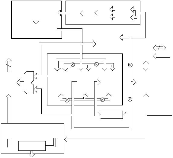
A block diagram of the MC68020/EC020 is shown in Figure 1-1.
1-2 |
M68020 USER’S MANUAL |
MOTOROLA |
|
|
|
SEQUENCER AND CONTROL |
INSTRUCTION PIPE |
|
|
|
|
|
|
|
|
|||||||||||||
|
|
|
|
|
|
|
|
|
|
|
|
|
|
|
|
|
|
|
CACHE |
|
|
|
|
|
|
|
|
|
CONTROL |
|
|
|
|
|
|
|
|
|
|
|
|
|
|
||||||||
|
|
|
|
|
|
STAGE |
|
|
STAGE |
|
|
STAGE |
|
|
HOLDING |
|
|
|
|
|
|||||
|
|
|
STORE |
|
|
|
D |
|
|
|
C |
|
|
|
B |
|
REGISTER |
|
|
|
|
|
|||
|
|
|
|
|
|
|
|
|
|
|
|
|
|
|
|
|
|
|
(CAHR) |
|
|
INTERNAL |
|||
|
|
|
|
|
|
|
|
|
|
|
|
|
|
|
|
|
|
||||||||
|
|
|
|
|
|
|
|
|
|
|
|
|
|
|
|
|
|
|
|
|
|
|
|||
|
|
|
|
|
|
|
|
|
|
|
|
|
|
|
|
|
|
|
|
|
|||||
|
|
|
|
|
|
|
|
|
|
|
|
|
|
|
|
|
|
|
|
|
|
|
DATA |
||
|
|
|
CONTROL |
|
|
|
|
|
|
|
|
|
|
|
|
|
|
|
|
|
|
|
BUS |
||
|
|
|
LOGIC |
|
|
|
|
|
|
|
|
|
|
|
|
|
|
|
|
|
|
|
|
|
|
|
|
|
|
|
|
|
|
|
|
|
|
|
INSTRUCTION |
|
|
|
|
|
|
||||||
|
|
|
|
|
|
|
|
|
|
|
|
|
|
|
|
|
|
|
|
|
|||||
|
|
|
|
|
|
|
|
|
|
|
|
|
|
|
|
|
|
|
|
|
|||||
|
|
|
|
|
|
|
|
|
|
|
|
|
|
|
|
CACHE |
|
|
|
|
|
|
32-BIT |
||
|
ADDRESS |
|
|
|
|
|
|
|
|
|
|
|
|
|
|
|
|
|
|
|
|
|
DATA |
|
|
|
|
|
|
|
|
|
|
|
|
|
|
|
|
|
|
|
|
|
|||||||
|
|
INSTRUCTION |
|
|
|
|
|
|
|
|
|
|
|
|
|
|
|
|
|
|
|
PADS |
|
|
|
|
BUS |
|
EXECUTION UNIT |
|
|
|
|
|
|
|
|
|
|
|
|
|
|
|
|
||||||
|
|
ADDRESS |
|
|
|
|
|
|
|
|
|
|
|
|
|
|
|
|
|
|
|||||
|
|
|
|
|
|
|
|
|
|
|
|
|
|
|
|
|
|
|
|
|
|
|
|
|
|
*32-BIT |
|
BUS |
|
|
|
|
|
|
|
|
|
|
|
|
|
|
|
|
|
|
|
|
|
|
|
|
|
|
|
|
|
|
|
|
|
|
|
|
|
|
|
|
|
|
|
|
|
|
|||
|
|
|
|
|
|
|
|
|
|
|
|
|
|
|
|
|
|
|
|
|
|
|
|
||
|
|
|
|
|
|
|
|
|
|
|
|
|
|
|
|
|
|
|
|
|
|
|
|
||
|
ADDRESS |
|
|
|
PROGRAM |
|
ADDRESS |
|
|
|
|
DATA |
|
|
|
|
|
SIZE |
|
||||||
|
|
|
|
COUNTER |
|
|
|
|
|
|
|
|
|
|
|||||||||||
|
PADS |
|
|
|
|
|
SECTION |
|
|
|
|
SECTION |
|
|
|
|
MULTIPLEXER |
|
|||||||
|
|
|
|
SECTION |
|
|
|
|
|
|
|
|
|
|
|||||||||||
|
|
|
|
|
|
|
|
|
|
|
|
|
|
|
|
|
|
|
|
|
|
|
|
||
|
|
|
|
|
|
|
|
|
|
|
|
|
|
|
|
|
|
|
|
|
|
|
|
|
|
ADDRESS
BUS
MISALIGNMENT
 MULTIPLEXER
BUS CONTROLLER
WRITE PENDING |
|
PREFETCH PENDING |
BUFFER |
|
BUFFER |
MICROBUS
CONTROL LOGIC 
BUS CONTROL
SIGNALS
* 24-Bit for MC68EC020
Figure 1-1. MC68020/EC020 Block Diagram
DATA BUS
MOTOROLA |
M68020 USER’S MANUAL |
1-3 |
1.2 PROGRAMMING MODEL
The programming model of the MC68020/EC020 consists of two groups of registers, the user model and the supervisor model, that correspond to the user and supervisor privilege levels, respectively. User programs executing at the user privilege level use the registers of the user model. System software executing at the supervisor level uses the control registers of the supervisor level to perform supervisor functions.
As shown in the programming models (see Figures 1-2 and 1-3), the MC68020/EC020 has 16 32-bit general-purpose registers, a 32-bit PC two 32-bit SSPs, a 16-bit SR, a 32-bit VBR, two 3-bit alternate function code registers, and two 32-bit cache handling (address and control) registers.
The user programming model remains unchanged from earlier M68000 family microprocessors. The supervisor programming model supplements the user programming model and is used exclusively by MC68020/EC020 system programmers who utilize the supervisor privilege level to implement sensitive operating system functions. The supervisor programming model contains all the controls to access and enable the special features of the MC68020/EC020. All application software, written to run at the nonprivileged user level, migrates to the MC68020/EC020 from any M68000 platform without modification.
Registers D7–D0 are data registers used for bit and bit field (1 to 32 bits), byte (8 bit), word (16 bit), long-word (32 bit), and quad-word (64 bit) operations. Registers A6–A0 and the USP, ISP, and MSP are address registers that may be used as software stack pointers or base address registers. Register A7 (shown as A7 in Figure 1-2 and as A7′ and A7″ in Figure 1-3) is a register designation that applies to the USP in the user privilege level and to either the ISP or MSP in the supervisor privilege level. In the supervisor privilege level, the active stack pointer (interrupt or master) is called the SSP. In addition, the address registers may be used for word and long-word operations. All of the 16 general-purpose registers (D7–D0, A7–A0) may be used as index registers.
The PC contains the address of the next instruction to be executed by the
MC68020/EC020. During instruction execution and exception processing, the processor automatically increments the contents of the PC or places a new value in the PC, as appropriate.
1-4 |
M68020 USER’S MANUAL |
MOTOROLA |
31 |
16 |
15 |
8 |
7 |
0 |
D0 |
|
D1 |
|
D2 |
|
D3 |
DATA |
|
|
D4 |
REGISTERS |
D5 |
|
D6 |
|
D7 |
|
31 |
16 |
15 |
0 |
A0
A1
A2
ADDRESS
A3
REGISTERS
A4
A5
A6
31 |
16 |
15 |
|
|
0 |
|
USER STACK |
|
|
|
|
|
|
A7 (USP) |
|
|
|
|
|
|
|
POINTER |
|
|
|
|
|
|
|
|
|
31 |
|
|
|
|
0 |
|
|
|
|
|
|
|
PROGRAM |
||
|
|
|
|
|
|
PC |
|
|
|
|
|
|
|
||
|
|
|
|
|
|
COUNTER |
|
|
|
|
|
|
|
|
|
|
|
15 |
8 |
7 |
0 |
|
CONDITION CODE |
|
|
|
0 |
|
|
CCR |
|
|
|
|
|
|
|||
|
|
|
|
|
REGISTER |
||
|
|
|
|
|
|
|
|
|
|
|
|
|
|
|
Figure 1-2. User Programming Model
MOTOROLA |
M68020 USER’S MANUAL |
1-5 |

31 |
16 |
15 |
|
|
|
0 |
|
INTERRUPT STACK |
|
|
|
|
|
|
|
A7' (ISP) |
|
|
|
|
|
|
|
|
POINTER |
|
|
|
|
|
|
|
|
|
|
31 |
16 |
15 |
|
|
|
0 |
|
|
|
|
|
|
MASTER STACK |
||||
|
|
|
|
|
|
|
A7'' (MSP) |
|
|
|
|
|
|
|
|
||
|
|
|
|
|
|
|
POINTER |
|
|
|
|
|
|
|
|
|
|
|
|
15 |
8 |
7 |
|
0 |
|
STATUS |
|
|
|
|
|
|
|
|
|
|
|
|
|
(CCR) |
|
|
SR |
|
|
|
|
|
|
|
REGISTER |
||
|
|
|
|
|
|
|
|
|
31 |
|
|
|
|
|
0 |
|
|
|
|
|
|
|
|
VECTOR BASE |
||
|
|
|
|
|
|
|
VBR |
|
|
|
|
|
|
|
|
||
|
|
|
|
|
|
|
REGISTER |
|
|
|
|
|
|
|
|
|
|
31 |
|
|
|
3 |
2 |
0 |
|
|
|
|
|
|
|
|
|
SFC |
ALTERNATE |
|
|
|
|
|
|
|
||
|
|
|
|
|
|
|
DFC |
FUNCTION CODE |
|
|
|
|
|
|
|
||
|
|
|
|
|
|
|
REGISTERS |
|
|
|
|
|
|
|
|
|
|
31 |
|
|
|
|
|
0 |
|
CACHE CONTROL |
|
|
|
|
|
|
|
CACR |
|
|
|
|
|
|
|
|
||
|
|
|
|
|
|
|
REGISTER |
|
|
|
|
|
|
|
|
|
|
31 |
|
|
|
|
|
0 |
|
|
|
|
|
|
|
|
CACHE ADDRESS |
||
|
|
|
|
|
|
|
CAAR |
|
|
|
|
|
|
|
|
||
|
|
|
|
|
|
|
REGISTER |
|
|
|
|
|
|
|
|
|
Figure 1-3. Supervisor Programming Model Supplement
1-6 |
M68020 USER’S MANUAL |
MOTOROLA |
The SR (see Figure 1-4) stores the processor status. It contains the condition codes that reflect the results of a previous operation and can be used for conditional instruction execution in a program. The condition codes are extend (X), negative (N), zero (Z), overflow (V), and carry (C). The user byte, which contains the condition codes, is the only portion of the SR information available in the user privilege level, and it is referenced as the CCR in user programs. In the supervisor privilege level, software can access the entire
SR, including the interrupt priority mask (three bits) and control bits that indicate whether the processor is in:
1.One of two trace modes (T1, T0)
2.Supervisor or user privilege level (S)
3.Master or interrupt mode (M)
|
|
|
|
|
|
|
|
|
|
|
|
|
USER BYTE |
|
|
|
|
||
|
|
|
|
SYSTEM BYTE |
|
|
|
(CONDITION CODE REGISTER) |
|
|
|||||||||
15 |
14 |
13 |
12 |
11 |
10 |
9 |
8 |
7 |
6 |
5 |
4 |
3 |
2 |
1 |
0 |
|
|||
|
|
|
|
|
|
|
|
|
|
|
|
|
|
|
|
|
|
|
|
|
T1 |
T0 |
S |
|
M |
0 |
I2 |
I1 |
I0 |
0 |
0 |
0 |
|
X |
N |
Z |
V |
C |
|
|
|
|
|
|
|
|
|
|
|
|
|
|
|
|
|
|
|
|
CARRY |
|
|
|
|
|
|
|
|
|
|
|
|
|
|
|
|
|
|
|
|
|
TRACE |
|
|
|
|
INTERRUPT |
|
|
|
|
|
|
|
|
|
OVERFLOW |
|||
|
ENABLE |
|
|
|
|
PRIORITY MASK |
|
|
|
|
|
|
|
|
|
||||
|
|
|
|
|
|
|
|
|
|
|
|
|
|
|
|
|
|
|
ZERO |
SUPERVISOR/USER LEVEL |
|
|
|
|
|
|
|
|
|
|
|
|
|
|
|
|
|
NEGATIVE |
|
MASTER/INTERRUPT MODE |
|
|
|
|
|
|
|
|
|
|
|
|
|
|
|
|
|
EXTEND |
|
Figure 1-4. Status Register (SR)
The VBR contains the base address of the exception vector table in memory. The displacement of an exception vector is added to the value in this register to access the vector table.
The alternate function code registers, SFC and DFC, contain 3-bit function codes. For the
MC68020, function codes can be considered extensions of the 32-bit linear address that optionally provide as many as eight 4-Gbyte address spaces; for the MC68EC020, function codes can be considered extensions of the 24-bit linear address that optionally provide as many as eight 16-Mbyte address spaces. Function codes are automatically generated by the processor to select address spaces for data and program at the user and supervisor privilege levels and to select a CPU address space for processor functions
(e.g., coprocessor communications). Registers SFC and DFC are used by certain instructions to explicitly specify the function codes for operations.
The CACR controls the on-chip instruction cache of the MC68020/EC020. The CAAR stores an address for cache control functions.
MOTOROLA |
M68020 USER’S MANUAL |
1-7 |
1.3 DATA TYPES AND ADDRESSING MODES OVERVIEW
For detailed information on the data types and addressing modes supported by the
MC68020/EC020, refer to M68000PM/AD, M68000 Family Programmer’s Reference
Manual.
The MC68020/EC020 supports seven basic data types:
1.Bits
2.Bit Fields (Fields of consecutive bits, 1–32 bits long)
3.BCD Digits (Packed: 2 digits/byte, Unpacked: 1 digit/byte)
4.Byte Integers (8 bits)
5.Word Integers (16 bits)
6.Long-Word Integers (32 bits)
7.Quad-Word Integers (64 bits)
In addition, the MC68020/EC020 instruction set supports operations on other data types such as memory addresses. The coprocessor mechanism allows direct support of floatingpoint operations with the MC68881 and MC68882 floating-point coprocessors as well as specialized user-defined data types and functions.
The 18 addressing modes listed in Table 1-1 include nine basic types:
1.Register Direct
2.Register Indirect
3.Register Indirect with Index
4.Memory Indirect
5.PC Indirect with Displacement
6.PC Indirect with Index
7.PC Memory Indirect
8.Absolute
9.Immediate
The register indirect addressing modes have postincrement, predecrement, displacement, and index capabilities. The PC modes have index and offset capabilities. Both modes are extended to provide indirect reference through memory. In addition to these addressing modes, many instructions implicitly specify the use of the CCR, stack pointer, and/or PC.
1-8 |
M68020 USER’S MANUAL |
MOTOROLA |

Table 1-1. Addressing Modes
|
|
Addressing Modes |
Syntax |
Register Direct |
|
||
Data |
|
|
Dn |
Address |
|
An |
|
Register Indirect |
|
||
Address |
|
(An) |
|
Address with Postincrement |
(An)+ |
||
Address with Predecrement |
–(An) |
||
Address with Displacement |
(d 16 , An) |
||
Address Register Indirect with Index |
|
||
8-Bit Displacement |
(d 8, An, Xn) |
||
Base Displacement |
(bd, An, Xn) |
||
Memory Indirect |
|
||
Postindexed |
([bd, An], Xn, od) |
||
Preindexed |
([bd, An, Xn], od) |
||
PC Indirect with Displacement |
(d 16 , PC) |
||
PC Indirect with Index |
|
||
8-Bit Displacement |
(d 8, PC, Xn) |
||
Base Displacement |
(bd, PC, Xn) |
||
PC Indirect |
|
|
|
Postindexed |
([bd, PC], Xn, od) |
||
Preindexed |
([bd, PC, Xn], od) |
||
Absolute Data Addressing |
|
||
Short |
|
|
(xxx).W |
Long |
|
|
(xxx).L |
Immediate |
|
|
#<data > |
NOTE: |
|
|
|
Dn |
= |
Data Register, D7–D0 |
|
An |
= |
Address Register, A7–A0 |
|
d8, d16 |
= |
A twos complement or sign-extended displacement added as part |
|
|
|
of the effective address calculation; size is 8 (d8) or 16 (d16 ) bits; |
|
|
|
when omitted, assemblers use a value of zero. |
|
Xn |
= |
Address or data register used as an index register; form is |
|
|
|
Xn.SIZE*SCALE, where SIZE is .W or .L (indicates index register |
|
|
|
size) and SCALE is 1, 2, 4, or 8 (index register is multiplied by |
|
|
|
SCALE); use of SIZE and/or SCALE is optional. |
|
bd |
= |
A twos-complement base displacement; when present, size can be |
|
|
|
16 or 32 bits. |
|
od |
= |
Outer displacement added as part of effective address calculation |
|
|
|
after any memory indirection; use is optional with a size of 16 or 32 |
|
|
|
bits. |
|
PC |
= |
Program Counter |
|
<data> |
= |
Immediate value of 8, 16, or 32 bits |
|
( ) |
= |
Effective Address |
|
[ ] |
= |
Use as indirect access to long-word address. |
|
MOTOROLA |
M68020 USER’S MANUAL |
1-9 |
1.4 INSTRUCTION SET OVERVIEW
For detailed information on the MC68020/EC020 instruction set, refer to M68000PM/AD,
M68000 Family Programmer’s Reference Manual.
The instructions in the MC68020/EC020 instruction set are listed in Table 1-2. The instruction set has been tailored to support structured high-level languages and sophisticated operating systems. Many instructions operate on bytes, words, or long words, and most instructions can use any of the 18 addressing modes.
1.5 VIRTUAL MEMORY AND VIRTUAL MACHINE CONCEPTS
The full addressing range of the MC68020 is 4 Gbytes (4,294,967,296 bytes) in each of eight address spaces; the full addressing range of the MC68EC020 is 16 Mbytes
(16,777,216 bytes) in each of the eight address spaces. Even though most systems implement a smaller physical memory, the system can be made to appear to have a full 4
Gbytes (MC68020) or 16 Mbytes (MC68EC020) of memory available to each user program by using virtual memory techniques.
In a virtual memory system, a user program can be written as if it has a large amount of memory available, although the physical memory actually present is much smaller. Similarly, a system can be designed to allow user programs to access devices that are not physically present in the system, such as tape drives, disk drives, printers, terminals, and so forth. With proper software emulation, a physical system can appear to be any other M68000 computer system to a user program, and the program can be given full access to all of the resources of that emulated system. Such an emulated system is called a virtual machine.
1.5.1 Virtual Memory
A system that supports virtual memory has a limited amount of high-speed physical memory that can be accessed directly by the processor and maintains an image of a much larger virtual memory on a secondary storage device such as a large-capacity disk drive. When the processor attempts to access a location in the virtual memory map that is not resident in physical memory, a page fault occurs. The access to that location is temporarily suspended while the necessary data is fetched from secondary storage and placed in physical memory. The suspended access is then either restarted or continued.
The MC68020/EC020 uses instruction continuation to support virtual memory. When a bus cycle is terminated with a bus error, the microprocessor suspends the current instruction and executes the virtual memory bus error handler. When the bus error handler has completed execution, it returns control to the program that was executing when the error was detected, reruns the faulted bus cycle (when required), and continues the suspended instruction.
1-10 |
M68020 USER’S MANUAL |
MOTOROLA |

Table 1-2. Instruction Set
Mnemonic |
Description |
Mnemonic |
Description |
ABCD |
Add Decimal with Extend |
MOVE USP |
Move User Stack Pointer |
ADD |
Add |
MOVEC |
Move Control Register |
ADDA |
Add Address |
MOVEM |
Move Multiple Registers |
ADDI |
Add Immediate |
MOVEP |
Move Peripheral |
ADDQ |
Add Quick |
MOVEQ |
Move Quick |
ADDX |
Add with Extend |
MOVES |
Move Alternate Address Space |
AND |
Logical AND |
MULS |
Signed Multiply |
ANDI |
Logical AND Immediate |
MULU |
Unsigned Multiply |
ASL, ASR |
Arithmetic Shift Left and Right |
NBCD |
Negate Decimal with Extend |
Bcc |
Branch Conditionally |
NEG |
Negate |
BCHG |
Test Bit and Change |
NEGX |
Negate with Extend |
BCLR |
Test Bit and Clear |
NOP |
No Operation |
BFCHG |
Test Bit Field and Change |
NOT |
Logical Complement |
BFCLR |
Test Bit Field and Clear |
OR |
Logical Inclusive OR |
BFEXTS |
Signed Bit Field Extract |
ORI |
Logical Inclusive OR Immediate |
BFEXTU |
Unsigned Bit Field Extract |
ORI CCR |
Logical Inclusive Or Immediate to Condition Codes |
BFFFO |
Bit Field Find First One |
ORI SR |
Logical Inclusive OR Immediate to Status Register |
BFINS |
Bit Field Insert |
PACK |
Pack BCD |
BFSET |
Test Bit Field and Set |
PEA |
Push Effective Address |
BFTST |
Test Bit Field |
RESET |
Reset External Devices |
BKPT |
Breakpoint |
ROL, ROR |
Rotate Left and Right |
BRA |
Branch Always |
ROXL,ROXR |
Rotate with Extend Left and Right |
BSET |
Test Bit and Set |
RTD |
Return and Deallocate |
BSR |
Branch to Subroutine |
RTE |
Return from Exception |
BTST |
Test Bit |
RTM |
Return from Module |
CALLM |
Call Module |
RTR |
Return and Restore Codes |
CAS |
Compare and Swap Operands |
RTS |
Return from Subroutine |
CAS2 |
Compare and Swap Dual Operands |
SBCD |
Subtract Decimal with Extend |
CHK |
Check Register Against Bound |
Scc |
Set Conditionally |
CHK2 |
Check Register Against Upper and Lower Bound |
STOP |
Stop |
CLR |
Clear |
SUB |
Subtract |
CMP |
Compare |
SUBA |
Subtract Address |
CMPA |
Compare Address |
SUBI |
Subtract Immediate |
CMPI |
Compare Immediate |
SUBQ |
Subtract Quick |
CMPM |
Compare Memory to Memory |
SUBX |
Subtract with Extend |
CMP2 |
Compare Register Against Upper and Lower Bounds |
SWAP |
Swap Register Words |
DBcc |
Test Condition, Decrement and Branch |
TAS |
Test and Set an Operand |
DIVS, DIVSL |
Signed Divide |
TRAP |
Trap |
DIVU, DIVUL |
Unsigned Divide |
TRAPcc |
Trap Conditionally |
EOR |
Logical Exclusive OR |
TRAPV |
Trap on Overflow |
EORI |
Logical Exclusive Or Immediate |
TST |
Test Operand |
EXG |
Exchange Registers |
UNLK |
Unlink |
EXT, EXTB |
Sign Extend |
UNPK |
Unpack BCD |
ILLEGAL |
Take Illegal Instruction Trap |
|
|
JMP |
Jump |
|
COPROCESSOR INSTRUCTIONS |
JSR |
Jump to Subroutine |
Mnemonic |
Description |
LEA |
Load Effective Address |
cpBcc |
Branch Conditionally |
LINK |
Link and Allocate |
cpDBcc |
Test Coprocessor Condition, Decrement and Branch |
LSL, LSR |
Logical Shift Left and Right |
cpGEN |
Coprocessor General Instruction |
MOVE |
Move |
cpRESTORE |
Restore Internal State of Coprocessor |
MOVEA |
Move Address |
cpSAVE |
Save Internal State of Coprocessor |
MOVE CCR |
Move Condition Code Register |
cpScc |
Set Conditionally |
MOVE SR |
Move Status Register |
cpTRAPcc |
Trap Conditionally |
MOTOROLA |
M68020 USER’S MANUAL |
1-11 |
1.5.2 Virtual Machine
A typical use for a virtual machine system is the development of software, such as an operating system, for a new machine also under development and not yet available for programming use. In a virtual machine system, a governing operating system emulates the hardware of the new machine and allows the new software to be executed and debugged as though it were running on the new hardware. Since the new software is controlled by the governing operating system, it is executed at a lower privilege level than the governing operating system. Thus, any attempts by the new software to use virtual resources that are not physically present (and should be emulated) are trapped to the governing operating system and performed by its software.
In the MC68020/EC020 implementation of a virtual machine, the virtual application runs at the user privilege level. The governing operating system executes at the supervisor privilege level and any attempt by the new operating system to access supervisor resources or execute privileged instructions causes a trap to the governing operating system.
Instruction continuation is used to support virtual I/O devices in memory-mapped input/output systems. Control and data registers for the virtual device are simulated in the memory map. An access to a virtual register causes a fault, and the function of the register is emulated by software.
1.6 PIPELINED ARCHITECTURE
The MC68020/EC020 contains a three-word instruction pipe where instruction opcodes are decoded. As shown in Figure 1-5, instruction words (instruction operation words and all extension words) enter the pipe at stage B and proceed to stages C and D. An instruction word is completely decoded when it reaches stage D of the pipe. Each stage has a status bit that reflects whether the word in the stage was loaded with data from a bus cycle that was terminated abnormally. Stages of the pipe are only filled in response to specific prefetch requests issued by the sequencer.
Words are loaded into the instruction pipe from the cache holding register. Although the individual stages of the pipe are only 16 bits wide, the cache holding register is 32 bits wide and contains the entire long word. This long word is obtained from the instruction cache or the external bus in response to a prefetch request from the sequencer. When the sequencer requests an even-word (long-word-aligned) prefetch, the entire long word is accessed from the instruction cache or the external bus and loaded into the cache holding register, and the high-order word is also loaded into stage B of the pipe. The instruction word for the next sequential prefetch can then be accessed directly from the cache holding register, and no external bus cycle or instruction cache access is required. The cache holding register provides instruction words to the pipe regardless of whether the instruction cache is enabled or disabled.
1-12 |
M68020 USER’S MANUAL |
MOTOROLA |
|
|
|
INSTRUCTION PIPE |
|
|
|
||
|
|
|
|
|
|
|
|
|
|
|
STAGE |
|
STAGE |
|
STAGE |
|
CACHE |
|
|
|
|
|
HOLDING |
|||
|
|
D |
|
C |
|
B |
|
|
|
|
|
|
|
REGISTER |
|||
|
|
|
|
|
|
|
|
|
|
|
|
|
|
|
|
|
|
|
|
|
|
|
|
|
|
|
SEQUENCER |
|
|
|
|
|
|
|
|
|
|
|
|
|
|
|
|
INSTRUCTION |
CONTROL |
|
|
|
|
|
|
|
FLOW FROM |
UNIT |
|
|
|
|
|
|
|
CACHE AND |
|
|
|
|
|
|
|
|
MEMORY |
|
|
|
|
|
|
|
|
|
EXECUTION
UNIT
Figure 1-5. Instruction Pipe
The sequencer is either executing microinstructions or awaiting completion of accesses that are necessary to continue executing microcode. The bus controller is responsible for all bus activity. The sequencer controls the bus controller, instruction execution, and internal processor operations such as the calculation of effective addresses and the setting of condition codes. The sequencer initiates instruction word prefetches and controls the validation of instruction words in the instruction pipe.
Prefetch requests are simultaneously submitted to the cache holding register, the instruction cache, and the bus controller. Thus, even if the instruction cache is disabled, an instruction prefetch may hit in the cache holding register and cause an external bus cycle to be aborted.
1.7 CACHE MEMORY
Due to locality of reference, instructions that are used in a program have a high probability of being reused within a short time. Additionally, instructions that reside in proximity to the instructions currently in use also have a high probability of being utilized within a short period. To exploit these locality characteristics, the MC68020/EC020 contains an on-chip instruction cache.
The cache improves the overall performance of the system by reducing the number of bus cycles required by the processor to fetch information from memory and by increasing the bus bandwidth available for other bus masters in the system.
MOTOROLA |
M68020 USER’S MANUAL |
1-13 |
SECTION 2
PROCESSING STATES
This section describes the processing states of the MC68020/EC020. It describes the functions of the bits in the supervisor portion of the SR and the actions taken by the processor in response to exception conditions.
Unless the processor has halted, it is always in either the normal or the exception processing state. Whenever the processor is executing instructions or fetching instructions or operands, it is in the normal processing state. The processor is also in the normal processing state while it is storing instruction results or communicating with a coprocessor.
NOTE
Exception processing refers specifically to the transition from normal processing of a program to normal processing of system routines, interrupt routines, and other exception handlers. Exception processing includes all stacking operations, the fetch of the exception vector, and the filling of the instruction pipe caused by an exception. Exception processing has completed when execution of the first instruction of the exception handler routine begins.
The processor enters the exception processing state when an interrupt is acknowledged, when an instruction is traced or results in a trap, or when some other exception condition arises. Execution of certain instructions or unusual conditions occurring during the execution of any instruction can cause exceptions. External conditions, such as interrupts, bus errors, and some coprocessor responses, also cause exceptions. Exception processing provides an efficient transfer of control to handlers and routines that process the exceptions.
A catastrophic system failure occurs whenever the processor receives a bus error or generates an address error while in the exception processing state. This type of failure halts the processor. For example, if during the exception processing of one bus error another bus error occurs, the MC68020/EC020 has not completed the transition to normal processing and has not completed saving the internal state of the machine; therefore, the processor assumes that the system is not operational and halts. Only an external reset can restart a halted processor. (When the processor executes a STOP instruction, it is in a special type of normal processing state—one without bus cycles. It is stopped, not halted.)
MOTOROLA |
M68020 USER’S MANUAL |
2-1 |
Loading...