


M68HC11
REFERENCE MANUAL
Motorola reserves the right to make changes without further notice to any products herein. Motorola makes no warranty, representation or guarantee regarding the suitability of its products for any particular purpose, nor does Motorola assume any liability arising out of the application or use of any product or circuit, and specifically disclaims any and all liability, including without limitation consequential or incidental damages. "Typical" parameters can and do vary in different applications. All operating parameters, including "Typicals" must be validated for each customer application by customer's technical experts. Motorola does not convey any license under its patent rights nor the rights of others. Motorola products are not designed, intended, or authorized for use as components in systems intended for surgical implant into the body, or other applications intended to support or sustain life, or for any other application in which the failure of the Motorola product could create a situation where personal injury or death may occur. Should Buyer purchase or use Motorola products for any such unintended or unauthorized application, Buyer shall indemnify and hold Motorola and its officers, employees, subsidiaries, affiliates, and distributors harmless against all claims, costs, damages, and expenses, and reasonable attorney fees arising out of, directly or indirectly, any claim of personal injury or death associated with such unintended or unauthorized use, even if such claim alleges that Motorola was negligent regarding the design or manufacture of the part. MOTOROLA and the Motorola logo are registered trademarks of Motorola, Inc. Motorola, Inc. is an Equal Opportunity/Affirmative Action Employer.
REV 3
© MOTOROLA, INC. 1996 PREVIOUS EDITIONS © 1991
TABLE OF CONTENTS
Paragraph |
Title |
Page |
|
|
|
SECTION 1GENERAL DESCRIPTION |
|
1.1 |
General Description of the MC68HC11A8 ................................................ |
1-1 |
|
1.2 |
Programmer’s Model ................................................................................. |
1-2 |
|
1.3 |
Product Derivatives ................................................................................... |
1-4 |
|
|
|
SECTION 2 PINS AND CONNECTIONS |
|
2.1 |
Packages And Pin Names ......................................................................... |
2-1 |
|
2.1.1 |
|
MC68HC11A8 ................................................................................... |
2-1 |
2.1.2 |
|
MC68HC11D3/711D3 ....................................................................... |
2-2 |
2.1.3 |
|
MC68HC11E9/711E9 ........................................................................ |
2-3 |
2.1.4 |
|
MC68HC811E2 ................................................................................. |
2-4 |
2.1.5 |
|
MC68HC11F1 ................................................................................... |
2-5 |
2.1.6 |
|
MC68HC24 Port Replacement Unit .................................................. |
2-6 |
2.2 |
Pin Descriptions ........................................................................................ |
2-7 |
|
2.2.1 |
|
Power-Supply Pins (VDD and VSS) .................................................. |
2-7 |
2.2.2 |
|
Mode Select Pins (MODB/VSTBY and MODA/LIR) .......................... |
2-8 |
2.2.3 |
|
Crystal Oscillator and Clock Pins (EXTAL, XTAL, and E) ............... |
2-10 |
2.2.4 |
|
Crystal Oscillator Application Information ........................................ |
2-15 |
2.2.4.1 |
|
Crystals for Parallel Resonance .............................................. |
2-15 |
2.2.4.2 |
|
Using Crystal Oscillator Outputs ............................................. |
2-15 |
2.2.4.3 |
|
Using External Oscillator ......................................................... |
2-15 |
2.2.4.4 |
|
AT-strip vs AT-cut Crystals ..................................................... |
2-16 |
2.2.5 |
|
Reset Pin (RESET) ......................................................................... |
2-16 |
2.2.6 |
|
Interrupt Pins (XIRQ, IRQ) .............................................................. |
2-17 |
2.2.7 |
|
A/D Reference and Port E Pins (VREFL, VREFH, PE[7:0]) ............ |
2-18 |
2.2.8 |
|
Timer Port A Pins ............................................................................ |
2-19 |
2.2.9 |
|
Serial Port D Pins ............................................................................ |
2-19 |
2.2.10 |
|
Ports B and C, STRA, and STRB Pins ............................................ |
2-20 |
2.3 |
Termination of Unused Pins .................................................................... |
2-21 |
|
2.4 |
Avoidance of Pin Damage ....................................................................... |
2-23 |
|
2.4.1 |
|
Zap and Latchup ............................................................................. |
2-24 |
2.4.2 |
|
Protective Interface Circuits ............................................................ |
2-24 |
2.4.3 |
|
Internal Circuitry — Digital Input-Only Pin ....................................... |
2-25 |
2.4.4 |
|
Internal Circuitry — Analog Input-Only Pin ...................................... |
2-26 |
2.4.5 |
|
Internal Circuitry — Digital I/O Pin ................................................... |
2-28 |
2.4.6 |
|
Internal Circuitry — Input/Open-Drain-Output Pin ........................... |
2-29 |
2.4.7 |
|
Internal Circuitry — Digital Output-Only Pin .................................... |
2-29 |
2.4.8 |
|
Internal Circuitry — MODB/VSTBY Pin ........................................... |
2-30 |
2.4.9 |
|
Internal Circuitry — IRQ/VPPBULK Pin .......................................... |
2-31 |
2.5 |
Typical Single-Chip-Mode System Connections ..................................... |
2-31 |
|
2.6 |
Typical Expanded-Mode-System Connections ....................................... |
2-33 |
|
M68HC11 |
|
|
MOTOROLA |
REFERENCE MANUAL |
iii |
||
TABLE OF CONTENTS
|
|
(Continued) |
|
Paragraph |
Title |
Page |
|
2.7 |
System Development and Debug Features ............................................ |
2-37 |
|
2.7.1 |
|
Load Instruction Register (LIR) ....................................................... |
2-37 |
2.7.2 |
|
Internal Read Visibility (IRV) ........................................................... |
2-37 |
2.7.3 |
|
MC68HC24 Port Replacement Unit ................................................ |
2-38 |
|
|
SECTION 3 CONFIGURATION AND MODES OF OPERATION |
|
3.1 |
Hardware Mode Selection ......................................................................... |
3-1 |
|
3.1.1 |
|
Hardware Mode Select Pins .............................................................. |
3-2 |
3.1.2 |
|
Mode Control Bits in the HPRIO Register ......................................... |
3-2 |
3.2 |
EEPROM-Based CONFIG Register .......................................................... |
3-3 |
|
3.2.1 |
|
Operation of CONFIG Mechanism .................................................... |
3-3 |
3.2.2 |
|
The CONFIG Register ....................................................................... |
3-4 |
3.3 |
Protected Control Register Bits ................................................................. |
3-6 |
|
3.3.1 |
|
RAM and I/O Mapping Register (INIT) .............................................. |
3-7 |
3.3.2 |
|
Protected Control Bits in the TMSK2 Register .................................. |
3-8 |
3.3.3 |
|
Protected Control Bits in the OPTION Register ................................ |
3-9 |
3.4 |
Normal MCU Operating Modes ............................................................... |
3-10 |
|
3.4.1 |
|
Normal Single-Chip Mode ............................................................... |
3-10 |
3.4.2 |
|
Normal Expanded Mode .................................................................. |
3-10 |
3.5 |
Special MCU Operating Modes ............................................................... |
3-11 |
|
3.5.1 |
|
Testing Functions Control Register (TEST1) .................................. |
3-12 |
3.5.2 |
|
Test-Related Control Bits in the BAUD Register ............................. |
3-14 |
3.5.3 |
|
Special Test Mode ........................................................................... |
3-14 |
3.5.4 |
|
Special Bootstrap Mode .................................................................. |
3-15 |
3.5.4.1 |
|
Loading Programs in Bootstrap Mode ..................................... |
3-16 |
3.5.4.2 |
|
Executing User Programs in Bootstrap Mode ......................... |
3-17 |
3.5.4.3 |
|
Using Interrupts in Bootstrap Mode ......................................... |
3-17 |
3.5.4.4 |
|
Bootloader Firmware Options ................................................. |
3-18 |
3.6 |
Test and Bootstrap Mode Applications .................................................... |
3-19 |
|
|
|
SECTION 4 ON-CHIP MEMORY |
|
4.1 |
ROM .......................................................................................................... |
4-1 |
|
4.2 |
RAM .......................................................................................................... |
4-2 |
|
4.2.1 |
|
Remapping Using the INIT Register .................................................. |
4-2 |
4.2.2 |
|
RAM Standby .................................................................................... |
4-3 |
4.3 |
EEPROM ................................................................................................... |
4-4 |
|
4.3.1 |
|
Logical and Physical Organization .................................................... |
4-4 |
4.3.2 |
|
Basic Operation of the EEPROM ...................................................... |
4-5 |
4.3.3 |
|
Systems Operating below 2-MHz Bus Speed (E Clock) ................... |
4-9 |
4.3.4 |
|
EEPROM Programming Register (PPROG) ................................... |
4-10 |
MOTOROLA |
|
M68HC11 |
|
iv |
|
REFERENCE MANUAL |
|
TABLE OF CONTENTS
|
|
(Continued) |
|
Paragraph |
Title |
Page |
|
4.3.5 |
|
Programming/Erasing Procedures .................................................. |
4-12 |
4.3.5.1 |
|
Programming ........................................................................... |
4-12 |
4.3.5.2 |
|
Bulk Erase ............................................................................... |
4-13 |
4.3.5.3 |
|
Row Erase ............................................................................... |
4-13 |
4.3.5.4 |
|
Byte Erase ............................................................................... |
4-13 |
4.3.5.5 |
|
CONFIG Register .................................................................... |
4-14 |
4.3.6 |
|
Optional EEPROM Security Mode .................................................. |
4-14 |
4.4 |
EEPROM Application Information ........................................................... |
4-16 |
|
4.4.1 |
|
Conditions and Practices to Avoid ................................................... |
4-16 |
4.4.2 |
|
Using EEPROM to Select Product Options ..................................... |
4-18 |
4.4.3 |
|
Using EEPROM for Setpoint and Calibration Information ............... |
4-18 |
4.4.4 |
|
Using EEPROM during Product Development ................................ |
4-19 |
4.4.5 |
|
Logging Data ................................................................................... |
4-19 |
4.4.6 |
|
Self-Adjusting Systems using EEPROM ......................................... |
4-20 |
4.4.7 |
|
Software Methods to Extend Life Expectancy ................................. |
4-21 |
|
|
SECTION 5 RESETS AND INTERRUPTS |
|
5.1 |
Initial Conditions Established During Reset .............................................. |
5-1 |
|
5.1.1 |
|
System Initial Conditions ................................................................... |
5-2 |
5.1.1.1 |
|
CPU ........................................................................................... |
5-2 |
5.1.1.2 |
|
Memory Map ............................................................................. |
5-2 |
5.1.1.3 |
|
Parallel I/O ................................................................................ |
5-2 |
5.1.1.4 |
|
Timer ......................................................................................... |
5-2 |
5.1.1.5 |
|
Real-Time Interrupt ................................................................... |
5-3 |
5.1.1.6 |
|
Pulse Accumulator .................................................................... |
5-3 |
5.1.1.7 |
|
COP Watchdog ......................................................................... |
5-3 |
5.1.1.8 |
|
Serial Communications Interface (SCI) ..................................... |
5-3 |
5.1.1.9 |
|
Serial Peripheral Interface (SPI) ............................................... |
5-3 |
5.1.1.10 |
|
Analog-to-Digital (A/D) Converter ............................................. |
5-3 |
5.1.1.11 |
|
Other System Controls .............................................................. |
5-4 |
5.1.2 |
|
CONFIG Register Allows Flexible Configuration ............................... |
5-4 |
5.1.3 |
|
Mode of Operation Established ......................................................... |
5-5 |
5.1.4 |
|
Program Counter Loaded with Reset Vector ..................................... |
5-5 |
5.2 |
Causes Of Reset ....................................................................................... |
5-5 |
|
5.2.1 |
|
Power-On Reset (POR) ..................................................................... |
5-7 |
5.2.2 |
|
COP Watchdog Timer Reset ............................................................. |
5-7 |
5.2.3 |
|
Clock Monitor Reset .......................................................................... |
5-9 |
5.2.4 |
|
External Reset ................................................................................. |
5-10 |
5.3 |
Interrupt Process ..................................................................................... |
5-11 |
|
5.3.1 |
|
Interrupt Recognition and Stacking Registers ................................. |
5-12 |
5.3.2 |
|
Selecting Interrupt Vectors .............................................................. |
5-12 |
5.3.3 |
|
Return from Interrupt ....................................................................... |
5-19 |
5.4 |
Non-Maskable Interrupts ......................................................................... |
5-20 |
|
5.4.1 |
|
Non-Maskable Interrupt Request (XIRQ) ........................................ |
5-20 |
M68HC11 |
|
|
MOTOROLA |
REFERENCE MANUAL |
v |
||
TABLE OF CONTENTS
|
|
(Continued) |
|
Paragraph |
Title |
Page |
|
5.4.2 |
|
Illegal Opcode Fetch ....................................................................... |
5-21 |
5.4.3 |
|
Software Interrupt ............................................................................ |
5-22 |
5.5 |
Maskable Interrupts ................................................................................. |
5-22 |
|
5.5.1 |
|
I Bit in the Condition Code Register ................................................ |
5-22 |
5.5.2 |
|
Special Considerations for I-Bit-Related Instructions ...................... |
5-23 |
5.6 |
Interrupt Request ..................................................................................... |
5-24 |
|
5.6.1 |
|
Selecting Edge Triggering or Level Triggering ................................ |
5-24 |
5.6.2 |
|
Sharing Vector with Handshake I/O Interrupts ................................ |
5-25 |
5.7 |
Interrupts from Internal Peripheral Subsystems ...................................... |
5-25 |
|
5.7.1 |
|
Inhibiting Individual Sources ............................................................ |
5-26 |
5.7.2 |
|
Clearing Interrupt Status Flag Bits .................................................. |
5-26 |
5.7.3 |
|
Automatic Clearing Mechanisms on Some Flags ............................ |
5-26 |
|
|
SECTION 6 CENTRAL PROCESSING UNIT |
|
6.1 |
Programmer’s Model ................................................................................. |
6-1 |
|
6.1.1 |
|
Accumulators (A, B, and D) ............................................................... |
6-1 |
6.1.2 |
|
Index Registers (X and Y) ................................................................. |
6-2 |
6.1.3 |
|
Stack Pointer (SP) ............................................................................. |
6-3 |
6.1.4 |
|
Program Counter (PC) ...................................................................... |
6-4 |
6.1.5 |
|
Condition Code Register (CCR) ........................................................ |
6-4 |
6.2 |
Addressing Modes ..................................................................................... |
6-6 |
|
6.2.1 |
|
Immediate (IMM) ............................................................................... |
6-6 |
6.2.2 |
|
Extended (EXT) ................................................................................. |
6-7 |
6.2.3 |
|
Direct (DIR) ....................................................................................... |
6-8 |
6.2.4 |
|
Indexed (INDX, INDY) ....................................................................... |
6-9 |
6.2.5 |
|
Inherent (INH) .................................................................................. |
6-10 |
6.2.6 |
|
Relative (REL) ................................................................................. |
6-10 |
6.3 |
M68HC11 Instruction Set ........................................................................ |
6-11 |
|
6.3.1 |
|
Accumulator and Memory Instructions ............................................ |
6-11 |
6.3.1.1 |
|
Loads, Stores, And Transfers ................................................. |
6-11 |
6.3.1.2 |
|
Arithmetic Operations .............................................................. |
6-12 |
6.3.1.3 |
|
Multiply and Divide .................................................................. |
6-13 |
6.3.1.4 |
|
Logical Operations .................................................................. |
6-13 |
6.3.1.5 |
|
Data Testing and Bit Manipulation .......................................... |
6-14 |
6.3.1.6 |
|
Shifts and Rotates ................................................................... |
6-14 |
6.3.2 |
|
Stack and Index Register Instructions ............................................. |
6-15 |
6.3.3 |
|
Condition Code Register Instructions .............................................. |
6-16 |
6.3.4 |
|
Program Control Instructions ........................................................... |
6-17 |
6.3.4.1 |
|
Branches ................................................................................. |
6-17 |
6.3.4.2 |
|
Jumps ...................................................................................... |
6-18 |
6.3.4.3 |
|
Subroutine Calls And Returns (BSR, JSR, RTS) .................... |
6-18 |
MOTOROLA |
|
M68HC11 |
|
vi |
|
|
REFERENCE MANUAL |
TABLE OF CONTENTS
|
|
(Continued) |
|
Paragraph |
Title |
Page |
|
6.3.4.4 |
|
Interrupt Handling (RTI, SWI, WAI) ......................................... |
6-18 |
6.3.4.5 |
|
Miscellaneous (NOP, STOP, TEST) ....................................... |
6-18 |
|
|
SECTION 7 PARALLEL INPUT/OUTPUT |
|
7.1 |
Parallel I/O Overview ................................................................................. |
7-1 |
|
7.2 |
Parallel I/O Register And Control Bit Explanations ................................... |
7-3 |
|
7.2.1 |
|
Port Registers .................................................................................... |
7-4 |
7.2.2 |
|
Data Direction Registers ................................................................... |
7-5 |
7.3 |
Detailed I/O Pin Descriptions .................................................................... |
7-6 |
|
7.3.1 |
|
Port A ................................................................................................ |
7-7 |
7.3.1.1 |
|
PA[2:0] (IC[3:1]) Pin Logic ......................................................... |
7-7 |
7.3.1.2 |
|
PA[6:3] (OC[5:2]) Pin Logic ....................................................... |
7-8 |
7.3.1.3 |
|
PA7 (OC1, PAI) Pin Logic ......................................................... |
7-9 |
7.3.1.4 |
|
Port A Idealized Timing ........................................................... |
7-12 |
7.3.2 |
|
Port B .............................................................................................. |
7-12 |
7.3.2.1 |
|
Port B Pin Logic ...................................................................... |
7-13 |
7.3.2.2 |
|
Port B Idealized Timing ........................................................... |
7-14 |
7.3.2.3 |
|
Special Considerations For Port B On MC68HC24 PRU ........ |
7-15 |
7.3.3 |
|
R/W (STRB) Pin .............................................................................. |
7-15 |
7.3.3.1 |
|
R/W (STRB) Pin Logic ............................................................ |
7-15 |
7.3.3.2 |
|
Special Considerations for STRB on MC68HC24 PRU .......... |
7-17 |
7.3.4 |
|
Port C .............................................................................................. |
7-17 |
7.3.4.1 |
|
Port C Pin Logic for Expanded Modes .................................... |
7-17 |
7.3.4.2 |
|
Summary of Port C Idealized Expanded-Mode Timing ........... |
7-18 |
7.3.4.3 |
|
Port C Single-Chip Mode Pin Logic ......................................... |
7-19 |
7.3.4.4 |
|
Port C Idealized Single-Chip Mode Timing ............................. |
7-23 |
7.3.4.5 |
|
Special Considerations for Port C on MC68HC24 PRU .......... |
7-24 |
7.3.5 |
|
AS (STRA) Pin ................................................................................ |
7-24 |
7.3.5.1 |
|
AS (STRA) Pin Logic ............................................................... |
7-24 |
7.3.5.2 |
|
Special Considerations for STRA on MC68HC24 PRU .......... |
7-26 |
7.3.6 |
|
Port D .............................................................................................. |
7-26 |
7.3.6.1 |
|
PD0 (RxD) Pin Logic ............................................................... |
7-26 |
7.3.6.2 |
|
PD1 (TxD) Pin Logic ............................................................... |
7-28 |
7.3.6.3 |
|
PD2 (MISO) Pin Logic ............................................................. |
7-30 |
7.3.6.4 |
|
PD3 (MOSI) Pin Logic ............................................................. |
7-32 |
7.3.6.5 |
|
PD4 (SCK) Pin Logic ............................................................... |
7-34 |
7.3.6.6 |
|
PD5 (SS) Pin Logic ................................................................. |
7-36 |
7.3.6.7 |
|
Idealized Port D Timing ........................................................... |
7-38 |
7.3.7 |
|
Port E .............................................................................................. |
7-40 |
7.3.7.1 |
|
Port E Pin Logic ...................................................................... |
7-40 |
7.3.7.2 |
|
Idealized Port E Timing ........................................................... |
7-41 |
7.4 |
Handshake I/O Subsystem ...................................................................... |
7-42 |
|
7.4.1 |
|
Simple Strobe Mode ........................................................................ |
7-43 |
7.4.1.1 |
|
Port B Strobe Output. .............................................................. |
7-43 |
M68HC11 |
|
|
MOTOROLA |
REFERENCE MANUAL |
vii |
||
TABLE OF CONTENTS
|
|
(Continued) |
|
Paragraph |
Title |
Page |
|
7.4.1.2 |
|
Port C Simple Latching Input .................................................. |
7-44 |
7.4.2 |
|
Full-input Handshake Mode ............................................................ |
7-44 |
7.4.3 |
|
Full-Output Handshake Mode ......................................................... |
7-45 |
7.4.3.1 |
|
Normal Output Handshake ...................................................... |
7-46 |
7.4.3.2 |
|
Three-State Variation of Output Handshake ........................... |
7-46 |
7.4.4 |
|
Parallel I/O Control Register (PIOC) ............................................... |
7-47 |
7.4.5 |
|
Non-Handshake Uses of STRA and STRB Pins ............................. |
7-49 |
|
SECTION 8 SYNCHRONOUS SERIAL PERIPHERAL INTERFACE |
|
|
8.1 |
SPI Transfer Formats ................................................................................ |
8-1 |
|
8.1.1 |
|
SPI Clock Phase and Polarity Controls ............................................. |
8-1 |
8.1.2 |
|
CPHA Equals Zero Transfer Format ................................................. |
8-2 |
8.1.3 |
|
CPHA Equals One Transfer Format .................................................. |
8-2 |
8.2 |
SPI Block Diagram .................................................................................... |
8-3 |
|
8.3 |
SPI Pin Signals .......................................................................................... |
8-4 |
|
8.4 |
SPI Registers ............................................................................................ |
8-6 |
|
8.4.1 |
|
Port D Data Direction Control Register (DDRD) ................................ |
8-6 |
8.4.2 |
|
SPI Control Register (SPCR) ............................................................ |
8-7 |
8.4.3 |
|
SPI Status Register (SPSR) .............................................................. |
8-8 |
8.5 |
SPI System Errors ..................................................................................... |
8-9 |
|
8.5.1 |
|
SPI Mode-Fault Error ........................................................................ |
8-9 |
8.5.2 |
|
SPI Write-Collision Errors ................................................................ |
8-10 |
8.6 |
Beginning and Ending SPI Transfers ...................................................... |
8-10 |
|
8.6.1 |
|
Transfer Beginning Period (Initiation Delay) .................................... |
8-10 |
8.6.2 |
|
Transfer Ending Period ................................................................... |
8-12 |
8.7 |
Transfers to Peripherals with Odd Word Lengths ................................... |
8-14 |
|
8.7.1 |
|
Example 8–1: On-Chip SPI Driving an MC144110 D/A .................. |
8-16 |
8.7.2 |
|
Example 8–2: Software SPI Driving an MC144110 D/A .................. |
8-16 |
SECTION 9 ASYNCHRONOUS SERIAL COMMUNICATIONS INTERFACE |
|||
9.1 |
General Description ................................................................................... |
9-1 |
|
9.1.1 |
|
Transmitter Block Diagram ................................................................ |
9-2 |
9.1.2 |
|
Receiver Block Diagram .................................................................... |
9-3 |
9.2 |
SCI Registers and Control Bits .................................................................. |
9-5 |
|
9.2.1Port D Related Registers and Control Bits (PORTD, DDRD, SPCR) 9-6
9.2.2 |
Baud-Rate Control Register (BAUD) |
.................................................9-7 |
9.2.3 |
SCI Control Register 1 (SCCR1) ....................................................... |
9-9 |
9.2.4 |
SCI Control Register 2 (SCCR2) ..................................................... |
9-10 |
9.2.5 |
SCI Status Register (SCSR) ........................................................... |
9-11 |
9.2.6 |
SCI Data Register (SCDR) .............................................................. |
9-14 |
MOTOROLA |
|
M68HC11 |
viii |
|
REFERENCE MANUAL |
TABLE OF CONTENTS
|
|
(Continued) |
|
Paragraph |
Title |
Page |
|
9.3 |
SCI Transmitter ....................................................................................... |
9-14 |
|
9.3.1 |
|
Eightand Nine-Bit Data Modes ...................................................... |
9-15 |
9.3.2 |
|
Interrupts and Status Flags ............................................................. |
9-16 |
9.3.3 |
|
Send Break ...................................................................................... |
9-16 |
9.3.4 |
|
Queued Idle Character .................................................................... |
9-17 |
9.3.5 |
|
Disabling the SCI Transmitter ......................................................... |
9-18 |
9.3.6 |
|
TxD Pin Buffer Logic ....................................................................... |
9-19 |
9.4 |
SCI Receiver ........................................................................................... |
9-20 |
|
9.4.1 |
|
Data Sampling Technique ............................................................... |
9-20 |
9.4.2 |
|
Worst-Case Baud-Rate Mismatch ................................................... |
9-26 |
9.4.3 |
|
Double-Buffered Operation ............................................................. |
9-28 |
9.4.4 |
|
Receive Status Flags and Interrupts ............................................... |
9-28 |
9.4.5 |
|
Receiver Wake-Up Operation ......................................................... |
9-29 |
9.4.5.1 |
|
Idle-Line Wake Up ................................................................... |
9-29 |
9.4.5.2 |
|
Address-Mark Wake Up .......................................................... |
9-29 |
9.5 |
Baud-Rate Generator .............................................................................. |
9-30 |
|
9.5.1 |
|
Timing Chain Block Diagram ........................................................... |
9-30 |
9.5.2 |
|
Baud Rates vs. Crystal Frequency .................................................. |
9-30 |
9.6 |
SCI Timing Details ................................................................................... |
9-30 |
|
9.6.1 |
|
Operation As Transmitter Is Enabled .............................................. |
9-31 |
9.6.2 |
|
TDRE and Transfers from SCDR to Transmit Shift Register .......... |
9-33 |
9.6.3 |
|
TC vs. Character Completion .......................................................... |
9-34 |
9.6.4 |
|
RDRF Flag Setting vs. End of a Received Character ..................... |
9-35 |
|
|
SECTION 10 MAIN TIMER AND REAL-TIME INTERRUPT |
|
10.1 |
General Description ................................................................................. |
10-1 |
|
10.1.1 |
|
Overall Timer Block Diagram .......................................................... |
10-2 |
10.1.2 |
|
Input-Capture Concept .................................................................... |
10-2 |
10.1.3 |
|
Output-Compare Concept ............................................................... |
10-4 |
10.2 |
Free-Running Counter and Prescaler ..................................................... |
10-5 |
|
10.2.1 |
|
Overall Clock Divider Structure ....................................................... |
10-5 |
10.2.1.1 |
|
Prescaler ................................................................................. |
10-7 |
10.2.1.2 |
|
Overflow ................................................................................ |
10-10 |
10.2.1.3 |
|
Counter Bypass (Test Mode) ................................................ |
10-11 |
10.2.2 |
|
Real-Time Interrupt (RTI) Function ............................................... |
10-11 |
10.2.3 |
|
COP Watchdog Function ............................................................... |
10-13 |
10.2.4 |
|
Tips for Clearing Timer Flags ........................................................ |
10-14 |
10.3 |
Input-Capture Functions ........................................................................ |
10-16 |
|
10.3.1 |
|
Programmable Options ................................................................. |
10-17 |
10.3.2 |
|
Using Input Capture to Measure Period and Frequency ............... |
10-18 |
10.3.3 |
|
Using Input Capture to Measure Pulse Width ............................... |
10-20 |
10.3.4 |
|
Measuring Very Short Time Periods ............................................. |
10-24 |
10.3.5 |
|
Measuring Long Time Periods with Input Capture and Overflow |
..10-24 |
10.3.6 |
|
Establishing a Relationship between Software and an Event ....... |
10-27 |
M68HC11 |
|
|
MOTOROLA |
REFERENCE MANUAL |
ix |
||
TABLE OF CONTENTS
|
|
(Continued) |
|
Paragraph |
Title |
Page |
|
10.3.7 |
|
Other Uses for Input-Capture Pins ................................................ |
10-28 |
10.4 |
Output-Compare Functions ................................................................... |
10-28 |
|
10.4.1 |
|
Normal I/O Pin Control Using OC[5:2] ........................................... |
10-32 |
10.4.2 |
|
Advanced I/O Pin Control Using OC1 ........................................... |
10-35 |
10.4.2.1 |
|
One Output Compare Controlling up to Five Pins ................. |
10-35 |
10.4.2.2 |
|
Two Output Compares Controlling One Pin .......................... |
10-36 |
10.4.3 |
|
Forced Output Compares .............................................................. |
10-38 |
10.5 |
Timing Details For The Main Timer System .......................................... |
10-39 |
|
10.6 |
Listing of Timer Examples ..................................................................... |
10-42 |
|
|
|
SECTION 11 PULSE ACCUMULATOR |
|
11.1 |
General Description ................................................................................. |
11-1 |
|
11.1.1 |
|
Pulse Accumulator Block Diagram .................................................. |
11-2 |
11.1.2 |
|
Pulse Accumulator Control and Status Registers ........................... |
11-3 |
11.2 |
Event Counting Mode .............................................................................. |
11-6 |
|
11.2.1 |
|
Interrupting after N Events .............................................................. |
11-6 |
11.2.2 |
|
Counting More Than 256 Events ..................................................... |
11-6 |
11.3 |
Gated Time Accumulation Mode ............................................................. |
11-8 |
|
11.3.1 |
|
Measuring Times Longer Than the Range of the 8-Bit Counter ...... |
11-8 |
11.3.2 |
|
Configuring for Interrupt after a Specified Time .............................. |
11-9 |
11.4 |
Other Uses for the PAI Pin ...................................................................... |
11-9 |
|
11.5 |
Timing Details for the Pulse Accumulator ............................................... |
11-9 |
|
|
|
SECTION 12 ANALOG-TO-DIGITAL CONVERTER SYSTEM |
|
12.1 |
Charge-Redistribution A/D ...................................................................... |
12-1 |
|
12.2 |
A/D Converter Implementation on MC68HC11A8 ................................. |
12-10 |
|
12.2.1 |
|
MC68HC11A8 Successive-Approximation A/D Converter ............ |
12-10 |
12.2.2 |
|
A/D Charge Pump and Resistor-Capacitor (RC) Oscillator ........... |
12-11 |
12.2.3 |
|
MC68HC11A8 A/D System Control Logic ..................................... |
12-13 |
12.2.4 |
|
A/D Control/Status Register (ADCTL) ........................................... |
12-14 |
12.2.5 |
|
A/D Result Registers (ADR[4:1]) ................................................... |
12-15 |
12.3 |
A/D Pin Connection Considerations ...................................................... |
12-16 |
|
|
|
APPENDIX A INSTRUCTION SET DETAILS |
|
A.1 |
Introduction ............................................................................................... |
A-1 |
|
A.2 |
Nomenclature ........................................................................................... |
A-1 |
|
|
|
APPENDIX BBOOTLOADER LISTINGS |
|
|
|
SUMMARY OF CHANGES |
|
MOTOROLA |
|
M68HC11 |
|
x |
|
REFERENCE MANUAL |
|
LIST OF ILLUSTRATIONS
Figure |
Title |
Page |
1-1 |
Block Diagram ................................................................................................ |
1-3 |
1-2 |
M68HC11 Programmer’s Model ..................................................................... |
1-4 |
1-3 |
Part Numbering .............................................................................................. |
1-5 |
2-1 |
MC68HC11A8 Pin Assignments .................................................................... |
2-2 |
2-2 |
MC68HC11D3/711D3 Pin Assignments ......................................................... |
2-3 |
2-3 |
MC68HC11E9/711E9 Pin Assignments (52-Pin PLCC) ................................. |
2-4 |
2-4 |
MC68HC811E2 Pin Assignments (48-Pin DIP) .............................................. |
2-5 |
2-5 |
MC68HC11F1 Pin Assignments (68-Pin PLCC) ............................................ |
2-6 |
2-6 |
MC68HC24 Pin Assignments ......................................................................... |
2-7 |
2-7 |
Reduced IDD MODA/LIR Connections .......................................................... |
2-9 |
2-8 |
RAM Standby MODB/VSTBY Connections .................................................. |
2-10 |
2-9 |
High-Frequency Crystal Connections ........................................................... |
2-12 |
2-10 |
Low-Frequency Crystal Connections ........................................................... |
2-12 |
2-11 |
Crystal Layout Example ............................................................................... |
2-13 |
2-12 |
Reset Circuit Example .................................................................................. |
2-17 |
2-13 |
Low-Pass Filter for A/D Reference Pins ....................................................... |
2-19 |
2-14 |
CMOS Inverter ............................................................................................. |
2-22 |
2-15 |
Internal Circuitry — Digital Input-Only Pin .................................................... |
2-25 |
2-16 |
Internal Circuitry — Analog Input-Only Pin ................................................... |
2-27 |
2-17 |
Internal Circuitry — Digital I/O Pin ................................................................ |
2-28 |
2-18 |
Internal Circuitry — Input/Open-Drain-Output Pin ........................................ |
2-29 |
2-19 |
Internal Circuitry — Output-Only Pin ............................................................ |
2-29 |
2-20 |
Internal Circuitry — MODB/VSTBY Pin ........................................................ |
2-30 |
2-21 |
Internal Circuitry — IRQ/VPPBULK Pin ....................................................... |
2-31 |
2-22 |
Basic Single-Chip-Mode Connections .......................................................... |
2-32 |
2-23 |
Basic Expanded Mode Connections (Sheet 1 of 2) ...................................... |
2-35 |
2–23 Basic Expanded Mode Connections (Sheet 2 of 2) ...................................... |
2-36 |
|
3-1 |
Schematic for Figure 3-2 (Sheet 1 of 2) ...................................................... |
3-21 |
3–1 |
Schematic for Figure 3-2 (Sheet 2 of 2) ...................................................... |
3-22 |
3-2 |
Program to Check/Change CONFIG ............................................................ |
3-23 |
4-1 |
Topological Arrangement of EEPROM Bytes (MC68HC11A8) ...................... |
4-5 |
4-2 |
Topological Arrangement of Bits in an EEPROM Byte ................................... |
4-5 |
4-3 |
Condensed Schematic of EEPROM Array ..................................................... |
4-6 |
4-4 |
EEPROM Cell Terminology ............................................................................ |
4-7 |
4-5 |
Erasing an EEPROM Byte ............................................................................. |
4-7 |
4-6 |
Programming an EEPROM Byte .................................................................... |
4-8 |
4-7 |
Reading an EEPROM Byte ............................................................................ |
4-9 |
4-8 |
Erase-Before-Write Programming Method ................................................... |
4-24 |
4-9 |
Program-More-Zeros Programming Method ................................................ |
4-24 |
4-10 |
Selective-Write Programming Method .......................................................... |
4-25 |
4-11 |
Composite Programming Method ................................................................. |
4-26 |
5-1 |
Typical External Reset Circuit ...................................................................... |
5-11 |
5-2 |
Processing Flow out of Resets (Sheet 1 of 2) .............................................. |
5-15 |
5–2 |
Processing Flow out of Resets (Sheet 2 of 2) .............................................. |
5-16 |
M68HC11 |
|
MOTOROLA |
REFERENCE MANUAL |
xi |
|
LIST OF ILLUSTRATIONS
|
(Continued) |
|
|
Figure |
Title |
|
Page |
5-3 |
Interrupt Priority Resolution (Sheet 1 of 2) ................................................... |
|
5-17 |
5–3 |
Interrupt Priority Resolution (Sheet 2 of 2) ................................................... |
|
5-18 |
5-4 |
Interrupt Source Resolution within SCI ........................................................ |
|
5-19 |
6-1 |
M68HC11 Programmer’s Model ..................................................................... |
|
6-2 |
7-1 |
Parallel I/O Registers and Control Bits ........................................................... |
|
7-3 |
7-2 |
Pin Logic Registers and Control Bits .............................................................. |
|
7-4 |
7-3 |
Special Symbols used in Pin Logic Diagrams ................................................ |
|
7-7 |
7-4 |
PA[2:0] (IC[3:1]) Pin Logic .............................................................................. |
|
7-8 |
7-5 |
PA[6:3] (OC[5:2]) Pin Logic .......................................................................... |
|
7-10 |
7-6 |
PA7 (OC1, PAI) Pin Logic ............................................................................ |
|
7-11 |
7-7 |
Idealized Port A Timing ................................................................................ |
|
7-12 |
7-8 |
Port B Pin Logic ............................................................................................ |
|
7-13 |
7-9 |
Idealized Port B Timing ................................................................................ |
|
7-14 |
7-10 |
R/W (STRB) Pin Logic .................................................................................. |
|
7-16 |
7-11 |
Port C Expanded Mode Pin Logic ................................................................ |
|
7-18 |
7-12 |
Summary of Idealized Port C Expanded-Mode Timing ................................ |
|
7-20 |
7-13 |
Port C Single-Chip Mode Pin Logic .............................................................. |
|
7-21 |
7-14 |
Idealized Port C Single-Chip Mode Timing .................................................. |
|
7-23 |
7-15 |
AS (STRA) Pin Logic .................................................................................... |
|
7-25 |
7-16 |
PD0 (RxD) Pin Logic .................................................................................... |
|
7-27 |
7-17 |
PD1 (TxD) Pin Logic ..................................................................................... |
|
7-29 |
7-18 |
PD2 (MISO) Pin Logic .................................................................................. |
|
7-31 |
7-19 |
PD3 (MOSI) Pin Logic .................................................................................. |
|
7-33 |
7-20 |
PD4 (SCK) Pin Logic .................................................................................... |
|
7-35 |
7-21 |
PD5 (SS) Pin Logic ...................................................................................... |
|
7-37 |
7-22 |
Idealized Port D Timing ................................................................................ |
|
7-39 |
7-23 |
Port E Pin Logic ............................................................................................ |
|
7-41 |
7-24 |
Idealized Port E Timing ................................................................................ |
|
7-42 |
7-25 |
Idealized Timing for Simple Strobe Operations ............................................ |
|
7-43 |
7-26 |
Idealized Timing for Full-Input Handshake ................................................... |
|
7-45 |
7-27 |
Idealized Timing for Full-Output Handshake ................................................ |
|
7-46 |
8-1 |
CPHA Equals Zero SPI Transfer Format ....................................................... |
|
8-2 |
8-2 |
CPHA Equals One SPI Transfer Format ........................................................ |
|
8-3 |
8-3 |
SPI System Block Diagram ............................................................................ |
|
8-4 |
8-4 |
Delay from Write SPDR to Transfer Start (Master) ...................................... |
|
8-12 |
8-5 |
Transfer Ending for an SPI Master ............................................................... |
|
8-13 |
8-6 |
Transfer Ending for an SPI Slave ................................................................. |
|
8-14 |
8-7 |
Hardware Hookup for Examples 8–1 and 8–2 ............................................. |
|
8-15 |
8-8 |
Register Definitions and RAM Variables for Examples 8–1 and 8–2 |
........... 8-16 |
|
8-9 |
Example 8–1 Software Listing (Sheet 1 of 2) ............................................... |
|
8-17 |
8–9 |
Example 8–1 Software Listing (Sheet 2 of 2) ............................................... |
|
8-18 |
MOTOROLA |
|
M68HC11 |
|
xii |
|
REFERENCE MANUAL |
|
LIST OF ILLUSTRATIONS
|
(Continued) |
|
Figure |
Title |
Page |
8-10 |
Timing Analysis for Example 8–1 ................................................................. |
8-19 |
8-11 |
Example 8–2 Software Listing ...................................................................... |
8-20 |
|
(a) EN Low to SCK Start Delay (MC144110 Needs 5 s) ............................ |
8-21 |
|
(b) Data to SCK Setup (MC144110 Needs 1 s) ......................................... |
8-21 |
8-12 |
Timing Analysis for Example 8–2 (Sheet 1 of 2) .......................................... |
8-21 |
|
(c) Data Hold vs. SCK (MC144110 Needs 5 s) .......................................... |
8-22 |
|
(d) SCK Low to EN Hold (MC144110 Needs 5 s) ...................................... |
8-22 |
8–12 Timing Analysis for Example 8-2 (Sheet 2 of 2) ........................................... |
8-22 |
|
9-1 |
SCI Transmitter Block Diagram ...................................................................... |
9-2 |
9-2 |
SCI Receiver Block Diagram .......................................................................... |
9-4 |
9-3 |
TxD Pin Logic Block Diagram ....................................................................... |
9-19 |
9-4 |
Start Bit — Ideal Case .................................................................................. |
9-22 |
9-5 |
Start Bit — Noise Case One ......................................................................... |
9-22 |
9-6 |
Start Bit — Noise Case Two ......................................................................... |
9-23 |
9-7 |
Start Bit — Noise Case Three ...................................................................... |
9-24 |
9-8 |
Start Bit — Noise Case Four ........................................................................ |
9-24 |
9-9 |
Start Bit — Noise Case Five ......................................................................... |
9-25 |
9-10 |
Start Bit — Noise Case Six .......................................................................... |
9-25 |
|
(a) Receive Data Slower Than Receiver Baud Rate .................................... |
9-27 |
|
(b) Receive Data Faster Than Receiver Baud Rate ..................................... |
9-27 |
9-11 |
Baud-Rate Frequency Tolerance ................................................................. |
9-27 |
9-12 |
Baud-Rate Generator Block Diagram ........................................................... |
9-31 |
9-13 |
Transmitter Enable Timing Details ............................................................... |
9-33 |
9-14 |
Write SCDR to Serial Data Start .................................................................. |
9-34 |
9-15 |
Ending Details of Transmission .................................................................... |
9-35 |
9-16 |
RDRF Flag-Setting Details ........................................................................... |
9-36 |
10-1 |
Main Timer System Block Diagram .............................................................. |
10-3 |
10-2 |
Timing Summary for Oscillator Divider Signals ............................................ |
10-6 |
10-3 |
Major Clock Divider Chains in the MC68HC11A8 ........................................ |
10-9 |
10-4 |
Measuring a Period with Input Capture ...................................................... |
10-19 |
10-5 |
Timing Analysis for Example 10–1 ............................................................. |
10-19 |
10-6 |
Measuring a Pulse Width with Input Capture ............................................. |
10-22 |
10-6 |
(a) Leading Edge Latency .......................................................................... |
10-23 |
10-6 |
(b) Process First Edge, Earliest Opportunity for Second Edge .................. |
10-23 |
10-7 |
Timing Analysis for Example 10–2 ............................................................. |
10-23 |
10-8 |
Measuring Long Periods with Input Capture and TOF (Sheet 1 of 2) ........ |
10-26 |
10-8 |
Measuring Long Periods with Input Capture and TOF (Sheet 2 of 2) ........ |
10-27 |
10-9 |
Simple Output-Compare Example .............................................................. |
10-31 |
10-10 |
Generating a Square Wave with Output Compare ..................................... |
10-33 |
10-11 |
Timing Analysis for Example 10–5 ............................................................. |
10-34 |
10-12 |
Producing Two PWM Outputs with OC1, OC2, and OC3 .......................... |
10-37 |
M68HC11 |
|
MOTOROLA |
REFERENCE MANUAL |
xiii |
|
LIST OF ILLUSTRATIONS
|
(Continued) |
|
Figure |
Title |
Page |
10-13 |
Timer Counter as MCU Leaves Reset ....................................................... |
10-40 |
10-14 |
Timer Counter Read — Cycle-by-Cycle Analysis ....................................... |
10-40 |
10-15 |
Input-Capture Timing Details ...................................................................... |
10-41 |
10-16 |
Output-Compare Timing Details ................................................................. |
10-42 |
11-1 |
Pulse Accumulator Operating Modes ........................................................... |
11-1 |
11-2 |
Block Diagram of Pulse Accumulator Subsystem ........................................ |
11-3 |
11-3 |
Pulse Accumulator Control and Status Register Summary .......................... |
11-4 |
11-4 |
PAI Pin Edge-Detection Timing .................................................................. |
11-10 |
11-5 |
Pin Enable vs. Counting (Gated Accumulation Mode) ............................... |
11-10 |
11-6 |
Timing Details for Pulse Accumulator Counter Overflow ........................... |
11-11 |
|
(a) PACNT Read ........................................................................................ |
11-12 |
|
(b) PACNT Write ........................................................................................ |
11-12 |
11-7 |
PACNT Read and Write ............................................................................. |
11-12 |
|
(a) Sample Mode .......................................................................................... |
12-2 |
|
(b) Hold Mode ............................................................................................... |
12-2 |
|
(c) Approximation Mode ............................................................................... |
12-2 |
12-1 |
Basic Charge-Redistribution A/D .................................................................. |
12-2 |
|
(a) Sample Mode .......................................................................................... |
12-8 |
|
(b) Hold Mode ............................................................................................... |
12-8 |
|
(c) Approximation Mode ............................................................................... |
12-8 |
12-2 |
Charge-Redistribution A/D with ± 1/2 LSB Quantization Error ..................... |
12-8 |
12-3 |
MC68HC11A8 A/D in Sample Mode .......................................................... |
12-11 |
12-4 |
Timing Diagram for a Sequence of Four A/D Conversions ........................ |
12-14 |
12-5 |
Electrical Model of an A/D Input Pin (Sample Mode) ................................. |
12-16 |
12-6 |
Graphic Estimation of Analog Sample Level (Case 2) ............................... |
12-19 |
MOTOROLA |
M68HC11 |
xiv |
REFERENCE MANUAL |
LIST OF TABLES
Table |
Title |
Page |
|
1-1 M68HC11 Family Members ................................................................................... |
|
1-6 |
|
2-1 Hardware Mode Select Summary.......................................................................... |
|
2-9 |
|
2-2 Ports B and C, STRA, and STRB Pins ................................................................ |
2-21 |
||
3-1 Hardware Mode Select Summary.......................................................................... |
|
3-2 |
|
3-2 |
Watchdog Rates vs. Crystal Frequency .............................................................. |
3-10 |
|
3-3 Bootstrap Mode Pseudo-Vectors......................................................................... |
|
3-18 |
|
5-1 Hardware Mode Select Summary.......................................................................... |
|
5-5 |
|
5-2 Reset Vector vs. Cause and MCU Mode............................................................... |
5-6 |
||
5-3 |
Watchdog Rates vs. Crystal Frequency ................................................................ |
5-8 |
|
5-4 |
Highest Priority 1 Interrupt vs. PSEL[3:0] ............................................................ |
5-14 |
|
9-1 |
Baud-Rate Prescale Selects.................................................................................. |
|
9-8 |
9-2 |
Baud-Rate Selects................................................................................................. |
|
9-9 |
9-3 Baud Rates by Crystal Frequency, SCP[1:0] and SCR[2:0] ................................ |
9-32 |
|
10-1 Crystal Frequency vs. PR1, PR0 Values ......................................................... |
10-10 |
|
10-2 |
RTI Rates vs. RTR1, RTR0 for Various Crystal Frequencies.......................... |
10-13 |
10-3 COP Time-Out vs. CR1, CR0 Values .............................................................. |
10-14 |
|
10-4 |
Instruction Sequences To Clear TOF .............................................................. |
10-15 |
11-1 |
Pulse Accumulator Timing Periods vs. Crystal Rate ......................................... |
11-2 |
12-1 |
A/D Channel Assignments............................................................................... |
12-15 |
M68HC11 |
MOTOROLA |
REFERENCE MANUAL |
xv |
LIST OF TABLES
|
(Continued) |
|
Table |
Title |
Page |
MOTOROLA |
M68HC11 |
xvi |
REFERENCE MANUAL |
SECTION 1GENERAL DESCRIPTION
This reference manual will be a valuable aid in the development of M68HC11 applications. Detailed descriptions of all internal subsystems and functions have been developed and carefully checked against internal Motorola design documentation, making this manual the most comprehensive reference available for the M68HC11 Family of microcontroller units (MCUs).
Practical applications are included to demonstrate the operation of each subsystem.
These applications are treated as complete systems, including hardware/software interactions and trade-offs. Interfacing techniques to prevent component damage are discussed to aid the hardware designer. For software programmers, SECTION 6 CENTRAL PROCESSING UNIT and APPENDIX A INSTRUCTION SET DETAILS contain examples demonstrating efficient use of the instruction set.
This manual is intended to complement Motorola’s official data sheet, not replace it. |
1 |
||
The information in the data sheet is current and is guaranteed by production testing. |
|||
Although the information in this manual was checked against parts and design docu- |
|||
mentation, the accuracy is not guaranteed like the data sheet is guaranteed. This man- |
|
||
ual assumes the reader has some basic knowledge of MCUs and assembly-language |
|
||
programming; it may not be appropriate as an instruction manual for a first-time MCU |
|
||
user. |
|
|
|
The information in this manual is much more detailed than would usually be required |
|
||
for normal use of the MCU, but a user who is familiar with the detailed operation of the |
|
||
part is more likely to find a solution to an unexpected system problem. In many cases, |
|
||
a trick based on software or on-chip resources can be used rather than building ex- |
|
||
pensive external circuitry. Data sheets are geared toward customary, straightforward |
|
||
use of the on-chip peripherals; whereas, an experienced MCU user often uses these |
|
||
on-chip systems in very unexpected ways. The level of detail in this manual will help |
|
||
the normal user to better understand the on-chip systems and will allow the more ad- |
|
||
vanced user to make maximum use of the subtleties of these systems. |
|
|
|
In addition to this manual, the data sheet(s) or technical summary is needed for the |
|
||
specific version(s) of the M68HC11 being used. A pocket reference guide is another |
|
||
beneficial source. |
|
|
|
1.1 General Description of the MC68HC11A8 |
|
|
|
The HCMOS MC68HC11A8 is an advanced 8-bit MCU with highly sophisticated, on- |
|
||
chip peripheral capabilities. New design techniques were used to achieve a nominal |
|
||
bus speed of 2 MHz. In addition, the fully static design allows operation at frequencies |
|
||
down to dc, further reducing power consumption. |
|
|
|
The HCMOS technology used on the MC68HC11A8 combines smaller size and higher |
|
||
speeds with the low power and high noise immunity of CMOS. On-chip memory sys- |
|
||
M68HC11 |
GENERAL DESCRIPTION |
MOTOROLA |
|
REFERENCE MANUAL |
|
1-1 |
|
|
tems include 8 Kbytes of read-only memory (ROM), 512 bytes of electrically erasable |
|
programmable ROM (EEPROM), and 256 bytes of random-access memory (RAM). |
|
Major peripheral functions are provided on-chip. An eight-channel analog-to-digital (A/ |
|
D) converter is included with eight bits of resolution. An asynchronous serial commu- |
|
nications interface (SCI) and a separate synchronous serial peripheral interface (SPI) |
|
are included. The main 16-bit, free-running timer system has three input-capture lines, |
|
five output-compare lines, and a real-time interrupt function. An 8-bit pulse accumula- |
|
tor subsystem can count external events or measure external periods. |
|
Self-monitoring circuitry is included on-chip to protect against system errors. A com- |
|
puter operating properly (COP) watchdog system protects against software failures. A |
|
clock monitor system generates a system reset in case the clock is lost or runs too |
|
slow. An illegal opcode detection circuit provides a non-maskable interrupt if an illegal |
|
opcode is detected. |
1 |
Two software-controlled power-saving modes, WAIT and STOP, are available to con- |
serve additional power. These modes make the M68HC11 Family especially attractive |
|
for automotive and battery-driven applications. |
|
Figure 1-1 is a block diagram of the MC68HC11A8 MCU. This diagram shows the ma- |
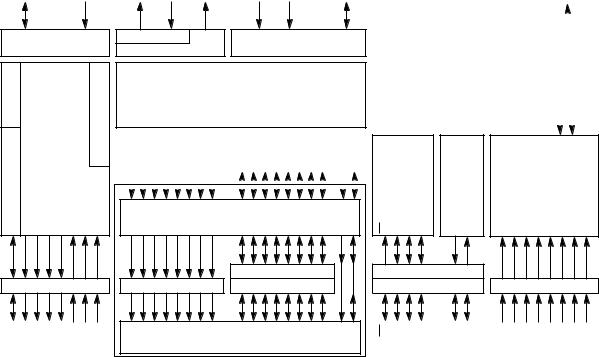
jor subsystems and how they relate to the pins of the MCU. In the lower right-hand corner of this diagram, the parallel I/O subsystem is shown inside a dashed box. The functions of this subsystem are lost when the MCU is operated in expanded modes, but the MC68HC24 port replacement unit can be used to regain the functions that were lost. The functions are restored in such a way that the software programmer is unable to tell any difference between a single-chip system or an expanded system containing the MC68HC24. By using an expanded system containing an MC68HC24 and an external EPROM, the user can develop software intended for a single-chip application.
1.2 Programmer’s Model
In addition to executing all M6800 and M6801 instructions, the M68HC11 instruction set includes 91 new opcodes. The nomenclature M68xx is used in conjunction with a specific CPU architecture and instruction set as opposed to the MC68HC11xx nomenclature, which is a reference to a specific member of the M68HC11 Family of MCUs.
Figure 1-2 shows the seven CPU registers available to the programmer. The two 8- bit accumulators (A and B) can be used by some instructions as a single 16-bit accumulator called the D register, which allows a set of 16-bit operations even though the
CPU is technically an 8-bit processor.
The largest group of instructions added involve the Y index register. Twelve bit manipulation instructions that can operate on any memory or register location were added. The exchange D with X and exchange D with Y instructions can be used to quickly get index values into the double accumulator (D) where 16-bit arithmetic can be used. Two 16-bit by 16-bit divide instructions are also included.
MOTOROLA |
GENERAL DESCRIPTION |
M68HC11 |
1-2 |
|
REFERENCE MANUAL |
MODA/ |
MODB/ |
|
|
LIR |
VSTBY |
|
|
MODE |
|
CONTROL |
|
COP |
|
INTERRUPT |
ACCUMULATOR |
|
PERIODIC |
|
|
TIMER |
|
SYSTEM |
|
PULSE |
|
|
|
PORT A |
|
PA7/PAI/OC1 PA6/OC2/OC1 PA5/OC3/OC1 |
PA4/OC4/OC1 PA3/OC5/OC1 PA2/IC1 PA1/IC2 PA0/IC3 |
|
|
|
|
|
|
|
|
XTAL EXTAL |
E |
IRQ/ XIRQ |
|
RESET |
||
OSCILLATOR
CLOCK LOGIC
INTERRUPT LOGIC
CPU
|
BUS EXPANSION |
|
ADDRESS/DATA |
|
R/W AS |
|||||||||||||||
|
|
ADDRESS |
|
|
||||||||||||||||
|
|
|
|
|
|
|
|
|
|
|
|
|||||||||
|
|
|
|
|
|
|
|
|
|
|
|
|
|
|
||||||
|
|
|
|
|
|
|
|
|
|
|
|
|
|
|
|
|
|
|
|
|
|
|
|
|
|
|
|
|
|
|
|
|
|
|
|
|
|
|
|
|
|
|
|
|
|
|
|
|
|
|
|
|
|
|
|
|
|
|
|
|
|
|
STROBE AND HANDSHAKE
PARALLEL I/O
|
|
|
|
CONTROL |
|
|
|
PORT B |
|
PORT C |
|
PB7 |
PB6 |
PB5 PB4 PB3 PB2 |
PB1 PB0 |
PC7 PC6 PC5 PC4 PC3 PC2 PC1 PC0 |
STRB STRA |
|
|
|
SINGLE CHIP MODE |
|
|
A15 A14 A13 A12 A11 A10 A9 A8 |
A7/D7 A6/D6 A5/D5 A4/D4 A3/D3 A2/D2 A1/D1 A0/D0 |
|
R/W AS |
|
|||
EXPANDED MODE |
|
|
|
CIRCUITRY ENCLOSED BY DOTTED LINE IS EQUIVALENT TO MC68HC24.
8 KBYTES ROM |
|
|
|
|
|
|
|
|
|
|
VDD |
|
|
|
|
|
|
|
|
|
|
||
|
|
|
|
|
|
|
|
|
|
|
|
|
|
|
|
|
|
|
|
|
|
|
|
|
|
|
|
|
|
|
|
|
|
|
VSS |
|
|
|
|
|
|
|
|
|
|
|
|
|
|
|
|
|
|
|
|
|
|
|
|
|
|
|
|
|
|
|
|
|
|
|
|
512 BYTES EEPROM |
|
|
|
|
|
|
|
|
|
|
|
|
|
|
|
|
|
|
|
|
|
|
VRH |
|
|
|
|
|
|
|
|
|
|
|
|
256 BYTES RAM |
|
|
|
|
|
|
|
|
|
|
|
|
|
|
|
|
|
|
|
|
|
VRL |
|
|
|
|
|
|
|
|
|
|
|
|
|
SPI |
|
SCI |
A/D CONVERTER |
|
|||
SS |
SCK |
MOSI |
MISO |
TxD |
RxD |
|
|
|
|
|
CONTROL |
|
|
|
1 |
||
|
|
PORT D |
|
|
PORT E |
|||
PD5/SS |
PD4/SCK |
PD3/MOSI |
PD2/MISO |
PD1/TxD |
PD0/RxD |
PE7/AN7 PE6/AN6 PE5/AN5 PE4/AN4 PE3/AN3 PE2/AN2 PE1/AN1 PE0/AN0 |
||
|
||||||||
Figure 1-1 Block Diagram
M68HC11 |
GENERAL DESCRIPTION |
MOTOROLA |
REFERENCE MANUAL |
|
1-3 |
|
7 |
A |
0 |
7 |
|
|
|
B |
0 |
|
8-BIT ACCUMULATORS A & B |
||||
|
15 |
|
D |
|
|
|
0 |
|
OR 16-BIT DOUBLE ACCUMULATOR D |
||||||
|
|
|
|
|
|
|
|
|
|
|
|
|
|
|
|
|
|
|
IX |
|
|
|
|
|
|
|
INDEX REGISTER X |
||||
|
|
|
|
|
|
|
|
|
|
|
|
|
|
|
|
|
|
|
IY |
|
|
|
|
|
|
|
INDEX REGISTER Y |
||||
|
|
|
|
|
|
|
|
|
|
|
|
|
|
|
|
|
|
|
SP |
|
|
|
|
|
|
|
STACK POINTER |
||||
|
|
|
|
|
|
|
|
|
|
|
|
|
|
|
|
|
|
|
PC |
|
|
|
|
|
|
|
PROGRAM COUNTER |
||||
|
|
|
7 |
|
|
|
|
|
|
0 |
|
|
|||
|
|
|
|
S X H |
I N Z |
V C |
|
CONDITION CODES |
|||||||
|
|
|
|
|
|
|
|
|
|
|
|
|
|
|
CARRY/BORROW FROM MSB |
|
|
|
|
|
|
|
|
|
|
|
|
|
|
|
|
|
|
|
|
|
|
|
|
|
|
|
|
|
|
|
|
|
|
|
|
|
|
|
|
|
|
|
|
|
|
|
OVERFLOW |
|
|
|
|
|
|
|
|
|
|
|
|
|
|
|
|
|
|
|
|
|
|
|
|
|
|
|
|
|
|
|
ZERO |
|
|
|
|
|
|
|
|
|
|
|
|
|
|
|
|
1 |
|
|
|
|
|
|
|
|
|
|
|
|
|
|
NEGATIVE |
|
|
|
|
|
|
|
|
|
|
|
|
|
|
||
|
|
|
|
|
|
|
|
|
|
|
|
|
|
I-INTERRUPT MASK |
|
|
|
|
|
|
|
|
|
|
|
|
|
|
|
||
|
|
|
|
|
|
|
|
|
|
|
|
|
|
HALF CARRY (FROM BIT 3) |
|
|
|
|
|
|
|
|
|
|
|
|
|
|
|
||
|
|
|
|
|
|
|
|
|
|
|
|
|
|
X-INTERRUPT MASK |
|
|
|
|
|
|
|
|
|
|
|
|
|
|
|
||
|
|
|
|
|
|
|
|
|
|
|
|
|
|
STOP DISABLE |
|
|
|
|
|
|
|
|
|
|
|
|
|
|
|
||
Figure 1-2 M68HC11 Programmer’s Model
1.3 Product Derivatives
The M68HC11 Family of MCUs is composed of several members (see Table 1-1), and new members are being developed. Figure 1-3 explains how the product part numbers are constructed.
MOTOROLA |
GENERAL DESCRIPTION |
M68HC11 |
1-4 |
|
REFERENCE MANUAL |

MC 68 HC P 7 11XX B C FN 3 R2
QUALIFICATION LEVEL
MC — FULLY SPECIFIED AND QUALIFIED
XC — PILOT PRODUCTION DEVICE
PC — ENGINEERING SAMPLE
NUMERIC DESIGNATOR (OPTIONAL)
OPERATING VOLTAGE RANGE
HC — HCMOS (VDD = 5.0 VDC ±10%)
L — HCMOS (VDD = 3.0 VDC TO 5.5 VDC)
COP OPTION (ONLY ON A-SERIES DEVICES)
NONE — COP DISABLED
P — COP ENABLED
MEMORY TYPE
BLANK — MASKED ROM OR NO ROM 7 — EPROM/OTPROM
8 — EEPROM
BASE PART NUMBER
11A8, 11D3, 11E9, 11K4, ETC.
MONITOR MASK
NONE — BLANK
B — BUFFALO
TEMPERATURE RANGE
NONE — 0°C TO 70°C
C — – 40°C TO 85°C
V — – 40°C TO 105°C
M — – 40°C TO 125°C
PACKAGE TYPE
FN — 44/52/68/84-PIN PLCC
FS — 44/52/68/84-PIN CLCC
FU — 64/80-PIN QFP
FB — 44-PIN QFP
PV — 112-PIN TQFP
PU — 80/100-PIN TQFP
PB — 52-PIN TQFP
P — 40/48-PIN DIP
S — 48-PIN SDIP
MAXIMUM SPECIFIED CLOCK SPEED
2 — 2.0 MHz
3 — 3.0 MHz
4 — 4.0 MHz
TAPE AND REEL OPTION
NONE — STANDARD PACKAGING
R2 — TAPE AND REEL PACKAGING
Figure 1-3 Part Numbering
M68HC11 |
GENERAL DESCRIPTION |
REFERENCE MANUAL
1
HC11 PART NUMBERING
MOTOROLA
1-5

Table 1-1 M68HC11 Family Members
|
Part Number |
EPROM |
ROM |
EEPROM |
RAM |
CONFIG2 |
Comments |
|
|
MC68HC11A8 |
— |
— |
512 |
256 |
$0F |
|
Family Built Around This Device |
|
|
|
|
|
|
|
|
|
|
MC68HC11A1 |
— |
— |
512 |
256 |
$0D |
’A8 with ROM Disabled |
|
|
|
|
|
|
|
|
|
|
|
MC68HC11A0 |
— |
— |
— |
256 |
$0C |
’A8 with ROM and EEPROM Disabled |
|
|
|
|
|
|
|
|
|
|
|
MC68HC811A8 |
— |
— |
8K + 512 |
256 |
$0F |
EEPROM Emulator for ’A8 |
|
|
|
|
|
|
|
|
|
|
|
MC68HC11E9 |
— |
12K |
512 |
512 |
$0F |
|
Four Input Capture/Bigger RAM 12K ROM |
|
|
|
|
|
|
|
|
|
|
MC68HC11E1 |
— |
— |
512 |
512 |
$0D |
’E9 with ROM Disabled |
|
|
|
|
|
|
|
|
|
|
|
MC68HC11E0 |
— |
— |
— |
512 |
$0C |
’E9 with ROM and EEPROM Disabled |
|
|
|
|
|
|
|
|
|
|
|
MC68HC811E2 |
— |
— |
2K1 |
256 |
$FF3 |
|
No ROM Part for Expanded Systems |
|
MC68HC711E9 |
12K |
— |
512 |
512 |
$0F |
|
One-Time Programmable Version of ’E9 |
|
|
|
|
|
|
|
|
|
|
MC68HC11D3 |
— |
4K |
— |
192 |
N/A |
Low-Cost 40-Pin Version |
|
|
|
|
|
|
|
|
|
|
|
MC68HC711D9 |
4K |
— |
— |
192 |
N/A |
One-Time Programmable Version of ’D3 |
|
1 |
|
|
|
|
|
|
|
|
MC68HC11F1 |
— |
— |
5121 |
1K |
$FF3 |
|
High-Performance Non-Multiplexed 6B-Pin |
|
MC68HC11K4 |
— |
24K |
640 |
768 |
$FF |
|
> 1 Mbyte memory space, PWM, C S, 84-Pin |
|
MC68HC711K4 |
24K |
— |
640 |
768 |
$FF |
|
One-Time Programmable Version of ’K4 |
|
|
|
|
|
|
|
|
|
|
MC68HC11L6 |
— |
16K |
512 |
512 |
$0F |
|
Like ’E9 with more ROM and more I/O, 64/68 |
|
|
|
|
|
|
|
|
|
|
|
MC68HC711L6 |
16K |
— |
512 |
512 |
$0F |
|
One-Time Programmable Version of ’L4 |
|
|
|
|
|
|
|
|
|
1.The EEPROM is relocatable to the top of any 4 Kbyte memory page. Relocation is done with the upper four bits of the CONFIG register.
2.CONFIG register values in this table reflect the value programmed prior to shipment from Motorola.
3.At the time of this printing a change was being considered that would make this value $0F.
MOTOROLA |
GENERAL DESCRIPTION |
M68HC11 |
1-6 |
|
REFERENCE MANUAL |
SECTION 2 PINS AND CONNECTIONS
This section discusses the functions of each pin on the MC68HC11A8. Most pins on this microcontroller unit (MCU) serve two or more functions. Information about the practical use of each pin is presented in these pin descriptions. This section also includes information concerning pins that are exposed to illegal levels or conditions. The most common source of illegal levels or conditions is transient noise; however, a designer may wish to take precautions against potential misapplication of a product or failures of other system components such as power supplies. Consideration of these factors can influence end-product reliability.
The basic connections for single-chip-mode and expanded-mode applications are presented in 2.5 Typical Single-Chip-Mode System Connections and 2.6 Typical Ex- panded-Mode-System Connections. These basic systems can be used as the
starting point for any user application and can minimize the time required to achieve a 2 working prototype system. The explanation of these basic systems includes informa-
tion concerning additions, such as additional memory on the expanded system.
System noise generation and susceptibility primarily depend on each system and its environment. The MC68HC11A8 is designed for higher bus speeds than earlier MCUs; since it is high-density complementary metal-oxide semiconductor (HCMOS), signals drive from rail to rail, unlike earlier N-channel metal-oxide semiconductor
(NMOS) processors. Since these factors can significantly affect noise issues, the system designer should consider these changes.
2.1 Packages And Pin Names
The following figures show pin assignments for several members of the M68HC11 MCU Family. The pin assignments for the MC68HC24 port replacement unit (PRU) are also presented for reference although the PRU is not discussed in detail in this manual.
Detailed mechanical data for packages may be found in the data sheets or technical summaries. Ordering information, which relates part number suffixes to package types and operating temperature range, are also found in the data sheets or technical summaries.
2.1.1 MC68HC11A8
The MC68HC11A8 is available in either a 52-pin plastic leaded chip carrier (PLCC) package or a 48-pin dual-in-line package (DIP). The silicon die is identical for both packages, but four of the analog-to-digital (A/D) converter inputs are not bonded out to pins in the 48-pin DIP. The MC68HC11A1 and MC68HC11A0 devices also use the same die as the MC68HC11A8, except that the contents of the nonvolatile CONFIG register determine whether or not internal read-only memory (ROM) and/or electrically erasable programmable ROM (EEPROM) are disabled. These downgraded device versions have identical pin assignments as the MC68HC11A8.
M68HC11 |
PINS AND CONNECTIONS |
MOTOROLA |
REFERENCE MANUAL |
|
2-1 |
2
Figure 2-1 shows the pin assignments for the MC68HC11A8 in the 52-pin PLCC package and the 48-pin DIP package.
|
|
|
|
|
|
|
|
|
STRB/R/W |
|
|
STRA/AS |
|
MODA/LIR |
|
STBY |
|
|
|
|
|
|
|
PE7/AN7 |
PE3/AN3 |
PE6/AN6 |
|
PE2/AN2 |
||||||
|
|
|
|
|
|
|
|
|
|
|
|
|
|
|
|
|
|
|
|
|||||||||||||||
|
|
|
|
|
|
EXTAL |
E |
|
MODB/V |
V |
V |
V |
|
|||||||||||||||||||||
|
|
|
|
|
|
|
||||||||||||||||||||||||||||
|
|
|
|
|
|
|
|
|
|
|
|
|
|
|
|
|
|
|
|
|
|
SS |
|
RH |
|
RL |
|
|
|
|
|
|
|
|
|
|
|
|
|
|
|
|
|
|
|
|
|
|
|
|
|
|
|
|
|
|
|
|
|
|
|
|
|
|
|
|
|
|
|
|
|
|
|
|
|
|
|
|
|
|
|
|
|
|
|
|
|
|
|
|
|
|
|
|
|
|
|
|
|
|
|
|
|
|
|
|
|
|
|
|
7 |
|
6 |
5 |
4 |
|
3 |
2 |
|
|
|
52 |
51 |
|
50 |
49 |
48 |
47 |
|||||||||||
|
|
XTAL |
8 |
|
|
|
|
|
|
|
|
|
|
|
|
|
|
1 |
|
|
|
|
|
|
|
|
|
|
|
|
||||
|
|
|
|
|
|
|
|
|
|
|
|
|
|
|
|
|
|
|
|
|
|
|
|
|
|
|
|
|||||||
|
|
|
|
|
|
|
|
|
|
|
|
|
|
|
|
|
|
|
|
|
|
|
|
|
|
|
|
|
|
|||||
|
|
|
|
|
|
|
|
|
|
|
|
|
|
|
|
|
|
|
|
|
|
|
|
|
|
|
|
|||||||
PC0/A0/D0 |
9 |
|
|
|
|
|
|
|
|
|
|
|
|
|
|
|
|
|
|
|
|
|
|
|
|
|
|
|
|
|||||
|
|
|
|
|
|
|
|
|
|
|
|
|
|
|
|
|
|
|
|
|
|
|
|
|
|
|||||||||
PC1/A1/D1 |
10 |
|
|
|
|
|
|
|
|
|
|
|
|
|
|
|
|
|
|
|
|
|
|
|
|
|
|
|
|
|||||
|
|
|
|
|
|
|
|
|
|
|
|
|
|
|
|
|
|
|
|
|
|
|
|
|
|
|||||||||
PC2/A2/D2 |
11 |
|
|
|
|
|
|
|
|
|
|
|
|
|
|
|
|
|
|
|
|
|
|
|
|
|
|
|
|
|||||
|
|
|
|
|
|
|
|
|
|
|
|
|
|
|
|
|
|
|
|
|
|
|
|
|
|
|||||||||
PC3/A3/D3 |
12 |
|
|
|
|
|
|
|
|
|
|
|
|
|
|
|
|
|
|
|
|
|
|
|
|
|
|
|
|
|||||
|
|
|
|
|
|
|
|
|
|
|
|
|
|
|
|
|
|
|
|
|
|
|
|
|
|
|||||||||
|
|
|
|
|
|
|
|
|
|
|
|
|
|
|
|
|
|
|
|
|
|
|
|
|
|
|||||||||
PC4/A4/D4 |
13 |
|
|
|
|
|
|
|
|
|
|
MC68HC11A8 |
|
|
|
|
|
|
|
|||||||||||||||
|
|
|
|
|
|
|
|
|
|
|
|
|
|
|
||||||||||||||||||||
PC5/A5/D5 |
14 |
|
|
|
|
|
|
|
|
|
|
|
|
|
|
|
|
|
||||||||||||||||
|
|
|
|
|
|
|
|
|
|
|
|
|
|
|
|
|
|
|
|
|
|
|
|
|
|
|
|
|||||||
PC6/A6/D6 |
15 |
|
|
|
|
|
|
|
|
|
|
|
|
|
|
|
|
|
|
|
|
|
|
|
|
|
|
|
|
|||||
|
|
|
|
|
|
|
|
|
|
|
|
|
|
|
|
|
|
|
|
|
|
|
|
|
|
|||||||||
PC7/A7/D7 |
16 |
|
|
|
|
|
|
|
|
|
|
|
|
|
|
|
|
|
|
|
|
|
|
|
|
|
|
|
|
|||||
|
|
|
|
|
|
|
|
|
|
|
|
|
|
|
|
|
|
|
|
|
|
|
|
|
|
|||||||||
|
|
|
|
|
|
|
|
|
|
|
|
|
|
|
|
|
|
|
|
|
|
|
|
|
|
|||||||||
|
|
|
|
|
|
17 |
|
|
|
|
|
|
|
|
|
|
|
|
|
|
|
|
|
|
|
|
|
|
|
|
|
|
|
|
|
RESET |
|
|
|
|
|
|
|
|
|
|
|
|
|
|
|
|
|
|
|
|
|
|
|
|
|
|
|||||||
|
|
|
|
|
|
|
|
|
|
|
|
|
|
|
|
|
|
|
|
|
|
|
|
|
|
|
|
|||||||
|
|
|
|
|
18 |
|
|
|
|
|
|
|
|
|
|
|
|
|
|
|
|
|
|
|
|
|
|
|
|
|
|
|
|
|
|
|
XIRQ |
|
|
|
|
|
|
|
|
|
|
|
|
|
|
|
|
|
|
|
|
|
|
|
|
|
|
|
|
||||
|
|
|
|
|
|
|
|
|
|
|
|
|
|
|
|
|
|
|
|
|
|
|
|
|
|
|
|
|
|
|||||
|
|
|
|
|
|
19 |
|
|
|
|
|
|
|
|
|
|
|
|
|
|
|
|
|
|
|
|
|
|
|
|
|
|
|
|
|
|
|
IRQ |
|
|
|
|
|
|
|
|
|
|
|
|
|
|
|
|
|
|
|
|
|
|
|
|
|
|
|
|
|||
|
|
|
20 |
|
|
|
|
|
|
|
|
|
|
|
|
|
|
|
|
|
|
|
|
|
|
|
|
|
|
|
|
|||
PD0/RxD |
|
|
|
|
|
24 |
|
|
|
|
|
|
27 |
28 |
29 |
|
30 |
|
|
32 |
33 |
|||||||||||||
|
|
|
|
|
|
|
|
|
|
|
|
|
|
|||||||||||||||||||||
|
|
|
|
|
|
21 |
|
22 |
23 |
25 |
26 |
|
31 |
|||||||||||||||||||||
|
|
|
|
|
|
|||||||||||||||||||||||||||||
|
|
|
|
|
|
|
|
|
|
|
|
|
|
|
|
|
|
|
|
|
|
|
|
|
|
|
|
|
|
|
||||
|
|
|
|
|
|
|
|
|
|
|
|
|
|
|
|
|
|
|
|
|
|
|
|
|
|
|
|
|
|
|
|
|
|
|
|
|
|
|
|
|
|
PD1/TxD |
PD2/MISO |
|
PD3/MOSI |
|
PD4/SCK |
|
|
PD5/SS |
|
V |
|
PA7/PAI/OC1 |
|
PA6/OC2/OC1 |
|
PA5/OC3/OC1 |
PA4/OC4/OC1 |
|
PA3/OC5/OC1 |
|
PA2/IC1 |
|
PA1/IC2 |
||||
|
|
|
|
|
|
|
|
|
|
|
|
|
|
|
|
|
|
|
DD |
|
|
|
|
|
|
|
|
|
|
|
|
|
|
|
46 PE5/AN5
45  PE1/AN1
44 PE4/AN4
43  PE0/AN0
42 PB0/A8
41  PB1/A9
40 PB2/A10
39  PB3/A11
38  PB4/A12
37  PB5/A13
36 PB6/A14
35  PB7/A15
34 PA0/IC3
PA7/PAI/OC1 |
|
1 |
48 |
|
|
VDD |
|
|
|||||||
|
|
|
|||||||||||||
|
|
||||||||||||||
PA6/OC2/OC1 |
|
2 |
47 |
|
|
PD5/SS |
|
||||||||
|
|
||||||||||||||
PA5/OC3/OC1 |
|
3 |
46 |
|
|
PD4/SCK |
|||||||||
|
|
|
|||||||||||||
|
|
||||||||||||||
PA4/OC4/OC1 |
|
4 |
45 |
|
|
PD3/MOSI |
|||||||||
|
|
||||||||||||||
|
|
||||||||||||||
PA3/OC5/OC1 |
|
5 |
44 |
|
|
PD2/MISO |
|||||||||
|
|
|
|||||||||||||
|
|
||||||||||||||
PA2/IC1 |
|
6 |
43 |
|
|
PD1/TxD |
|||||||||
|
|
||||||||||||||
|
|
||||||||||||||
PA1/IC2 |
|
7 |
42 |
|
|
PD0/RxD |
|||||||||
|
|
|
|||||||||||||
|
|
||||||||||||||
PA0/IC3 |
|
|
|
|
|
|
|
|
|
||||||
|
8 |
41 |
|
|
IRQ |
||||||||||
|
|
||||||||||||||
PB7/A15 |
|
|
40 |
|
|
|
|
|
|
|
|
|
|||
|
9 |
|
|
XIRQ |
|||||||||||
|
|
||||||||||||||
PB6/A14 |
|
|
|
|
|
|
|
|
|
|
|
|
|
||
|
10 |
39 |
|
|
RESET |
||||||||||
|
|
||||||||||||||
PB5/A13 |
|
11 |
38 |
|
|
PC7/A7/D7 |
|||||||||
|
|
||||||||||||||
|
|
|
MC68HC11A8 |
|
|
PC6/A6/D6 |
|||||||||
PB4/A12 |
|
12 |
37 |
|
|
||||||||||
PB3/A11 |
|
13 |
36 |
|
|
PC5/A5/D5 |
|||||||||
|
|
||||||||||||||
|
|
||||||||||||||
PB2/A10 |
|
14 |
35 |
|
|
PC4/A4/D4 |
|||||||||
|
|
||||||||||||||
PB1/A9 |
|
15 |
34 |
|
|
PC3/A3/D3 |
|||||||||
|
|
||||||||||||||
|
|
||||||||||||||
PB0/A8 |
|
16 |
33 |
|
|
PC2/A2/D2 |
|||||||||
|
|
||||||||||||||
PE0/AN0 |
|
17 |
32 |
|
|
PC1/A1/D1 |
|||||||||
|
|
||||||||||||||
|
|
||||||||||||||
PE1/AN1 |
|
18 |
31 |
|
|
PC0/A0/D0 |
|||||||||
|
|
||||||||||||||
|
|
|
XTAL |
||||||||||||
PE2/AN2 |
|
19 |
30 |
|
|
||||||||||
|
|
||||||||||||||
|
|
||||||||||||||
PE3/AN3 |
|
20 |
29 |
|
|
EXTAL |
|||||||||
|
|
||||||||||||||
VRL |
|
21 |
28 |
|
|
STRB/R/W |
|
|
|
||||||
|
|
|
|
||||||||||||
|
|
||||||||||||||
VRH |
|
22 |
27 |
|
|
E |
|||||||||
|
|
||||||||||||||
VSS |
|
23 |
26 |
|
|
STRA/AS |
|||||||||
|
|
||||||||||||||
|
|
||||||||||||||
MODB/VSTBY |
|
24 |
25 |
|
|
|
|
|
|
|
|
||||
|
|
|
MODA/LIR |
||||||||||||
|
|
||||||||||||||
Figure 2-1 MC68HC11A8 Pin Assignments
2.1.2 MC68HC11D3/711D3
The MC68HC11D3 is available in either a 44-pin PLCC package or a 40-pin DIP package. The silicon die is identical for both packages, but the PLCC version has two additional output compare pins bonded out and an extra VSS pin named EVSS. The MC68HC711D3 is functionally equivalent to the MC68HC11D3 but has 4 Kbytes of EPROM instead of mask programmed ROM. The MC68HC711D3 is available as a one-time-programmable (OTP) MCU in an opaque plastic package or in a ceramic windowed package for development applications.
Figure 2-2 shows the pin assignments for the MC68HC11D3/711D3 in the 44-pin PLCC package and the 40-pin DIP package.
MOTOROLA |
PINS AND CONNECTIONS |
M68HC11 |
2-2 |
|
REFERENCE MANUAL |
|
|
|
|
|
|
|
|
|
|
|
|
|
|
|
|
STRB/R/W |
|
|
|
|
|
|
STRA/AS |
|
MODA/LIR |
|
STBY |
|
|
|
|
|
|
|
|
|
|
|
|
|
|
PE7/AN7 |
|
|
PE3/AN3 |
|
|
|
|
|
|
VSS |
|
1 |
|
||||||||||||||
|
|
|
|
|
|
|
|
|
|
|
|
|
|
|
|
|
|
|
|
|
|
|
|
|
|
|
|
|
|
|
|
|
|
|
|
|
|
|
|
|
|
|
|
|
|
|
|
||||||||||||||||||||||
|
|
|
|
|
|
|
|
|
|
|
|
|
|
|
|
|
|
|
|
|
|
|
|
|
|
|
|
|
|
|
|
|
|
|
|
|
|
|
|
|
|
|
|
|
|
|
|
||||||||||||||||||||||
|
|
|
|
|
|
|
|
|
|
|
|
EXTAL |
|
E |
|
|
|
|
|
MODB/V |
V |
|
V |
|
V |
|
|
|
|
|
PC1/ADDR1 |
|
3 |
|
|||||||||||||||||||||||||||||||||||
|
|
|
|
|
|
|
|
|
|
|
|
|
|
|
|
|
|
|
|
|
|
|
|
|
|
|
|
|
|
|
|
|
|
|
|
|
SS |
|
|
|
RH |
|
|
|
RL |
|
|
|
|
|
|
|
|
|
|
|
PC0/ADDR0 |
|
2 |
|
|||||||||
|
|
|
|
|
|
|
|
|
|
|
|
|
|
|
|
|
|
|
|
|
|
|
|
|
|
|
|
|
|
|
|
|
|
|
|
|
|
|
|
|
|
|
|
|
|
|
|
|
|
|
|
|
|
|
|
||||||||||||||
|
|
|
|
|
|
|
|
|
|
|
|
|
|
|
|
|
|
|
|
|
|
|
|
|
|
|
|
|
|
|
|
|
|
|
|
|
|
|
|
|
|
|
|
|
|
|
|
|
|
|
|
|
|
PC2/ADDR2 |
|
4 |
|
||||||||||||
|
|
|
|
|
|
|
|
|
|
|
|
|
|
|
|
|
|
|
|
|
|
|
|
|
|
|
|
|
|
|
|
|
|
|
|
|
|
|
|
|
|
|
|
|
|
|
|
|
|
|
|
|
|
|
|
||||||||||||||
|
|
|
|
|
|
|
|
|
|
|
|
|
|
|
|
|
|
|
|
|
|
|
|
|
|
|
|
|
|
|
|
|
|
|
|
|
|
|
|
|
|
|
|
|
|
|
|
|
|
|
|
|
|
|
|
|
|
|
|
|
|||||||||
|
|
|
|
|
|
|
|
6 |
|
|
|
5 |
|
4 |
3 |
|
|
2 |
|
|
|
|
|
|
44 |
43 |
42 |
|
|
41 |
40 |
|
|
|
|
|
|
|
|||||||||||||||||||||||||||||||
|
|
|
|
|
|
|
|
|
|
|
|
|
|
|
|
|
|
|
|
|
|
|
|
|
|
|
PC3/ADDR3 |
|
|
|
|||||||||||||||||||||||||||||||||||||||
PC4/ADDR4 |
|
7 |
|
|
|
|
|
|
|
|
|
|
|
|
|
|
|
|
|
|
|
|
|
1 |
|
|
|
|
|
|
|
|
|
|
|
|
|
|
|
|
|
39 |
|
PB0/ADDR8 |
|
5 |
|
||||||||||||||||||||||
PC5/ADDR5 |
|
8 |
|
|
|
|
|
|
|
|
|
|
|
|
|
|
|
|
|
|
|
|
|
|
|
|
|
|
|
|
|
|
|
|
|
|
|
|
|
|
|
|
38 |
|
PB1/ADDR9 |
PC4/ADDR4 |
|
6 |
|
||||||||||||||||||||
|
|
|
|
|
|
|
|
|
|
|
|
|
|
|
|
|
|
|
|
|
|
|
|
|
|
|
|
|
|
|
|
|
|
|
|
|
|
|
|
|
|
|
|
||||||||||||||||||||||||||
|
|
|
|
|
|
|
|
|
|
|
|
|
|
|
|
|
|
|
|
|
|
|
|
|
|
|
|
|
|
|
|
|
|
|
|
|
|
|
|
|
|
|
|
||||||||||||||||||||||||||
|
|
|
|
|
|
|
|
|
|
|
|
|
|
|
|
|
|
|
|
|
|
|
|
|
|
|
|
|
|
|
|
|
|
|
|
|
|
|
|
|
|
|
|||||||||||||||||||||||||||
|
|
|
|
|
|
|
|
|
|
|
|
|
|
|
|
|
|
|
|
|
|
|
|
|
|
|
|
|
|
|
|
|
|
|
|
|
|
|
|
|
|
|
|
||||||||||||||||||||||||||
PC6/ADDR6 |
|
9 |
|
|
|
|
|
|
|
|
|
|
|
|
|
|
|
|
|
|
|
|
|
|
|
|
|
|
|
|
|
|
|
|
|
|
|
|
|
|
|
|
37 |
|
PB2/ADDR10 PC5/ADDR5 |
|
7 |
MC68HC(7)11D3 |
|||||||||||||||||||||
|
|
|
|
|
|
|
|
|
|
|
|
|
|
|
|
|
|
|
|
|
|
|
|
|
|
|
|
|
|
|
|
|
|
|
|
|
|
|
|
|
|
|
|||||||||||||||||||||||||||
PC7/ADDR7 |
|
10 |
|
|
|
|
|
|
|
|
|
|
|
|
|
|
|
|
|
|
|
|
|
|
|
|
|
|
|
|
|
|
|
|
|
|
|
|
|
|
|
36 |
|
PB3/ADDR11 PC6/ADDR6 |
|
8 |
|||||||||||||||||||||||
|
|
|
|
|
|
|
|
11 |
|
|
|
|
|
|
|
|
|
|
|
|
|
|
|
|
|
|
|
|
|
|
|
|
|
|
|
|
|
|
|
|
|
|
|
|
|
|
|
35 |
|
PB4/ADDR12 PC7/ADDR7 |
|
9 |
|
||||||||||||||||
|
XIRQ/VPP |
|
12 |
|
|
|
|
|
|
|
|
|
|
|
|
|
MC68HC(7)11D3 |
|
|
|
|
|
|
|
|
|
|
|
|
|
|
|
|
|
|
||||||||||||||||||||||||||||||||||
|
PD7/R/W |
|
|
|
|
|
|
|
|
|
|
|
|
|
|
|
|
|
|
|
|
|
|
|
|
34 |
|
PB5/ADDR13 |
|
XIRQ |
/VPP |
|
10 |
|
|||||||||||||||||||||||||||||||||||
|
|
|
|
|
|
|
|
|
|
|
|
|
|
|
|
|
|
|
|
|
|
|
|
|
|
|
|
|
|
|
|
|
|
|
|
|
|
|
|
|
|
|
|
|
|
|
|||||||||||||||||||||||
|
PD6/AS |
|
13 |
|
|
|
|
|
|
|
|
|
|
|
|
|
|
|
|
|
|
|
|
|
|
|
|
|
|
|
|
|
|
|
|
|
|
|
|
|
|
|
33 |
|
PB6/ADDR14 |
|
PD7/R/W |
|
|
|
11 |
|
|||||||||||||||||
|
|
|
|
|
|
|
|
|
|
|
|
|
|
|
|
|
|
|
|
|
|
|
|
|
|
|
|
|
|
|
|
|
|
|
|
|
|
|
|
|
|
|
|
|
|
|
|||||||||||||||||||||||
|
|
|
|
|
|
|
|
|
|
|
|
|
|
|
|
|
|
|
|
|
|
|
|
|
|
|
|
|
|
|
|
|
|
|
|
|
|
|
|
|
|
|
|||||||||||||||||||||||||||
|
|
|
|
|
|
|
|
14 |
|
|
|
|
|
|
|
|
|
|
|
|
|
|
|
|
|
|
|
|
|
|
|
|
|
|
|
|
|
|
|
|
|
|
|
|
|
|
|
32 |
|
PB7/ADDR15 |
|
PD6/AS |
|
12 |
|
||||||||||||||
|
|
RESET |
|
|
|
|
|
|
|
|
|
|
|
|
|
|
|
|
|
|
|
|
|
|
|
|
|
|
|
|
|
|
|
|
|
|
|
|
|
|
|
|
|
|
|
|
|
||||||||||||||||||||||
|
|
|
|
|
|
|
|
|
|
|
|
|
|
|
|
|
|
|
|
|
|
|
|
|
|
|
|
|
|
|
|
|
|
|
|
|
|
|
|
|
|
|
|
|
|
|
|||||||||||||||||||||||
|
|
|
|
|
|
|
|
15 |
|
|
|
|
|
|
|
|
|
|
|
|
|
|
|
|
|
|
|
|
|
|
|
|
|
|
|
|
|
|
|
|
|
|
|
|
|
|
|
31 |
|
NC |
|
|
|
|
|
|
|
13 |
|
||||||||||
|
|
|
|
IRQ |
|
|
|
|
|
|
|
|
|
|
|
|
|
|
|
|
|
|
|
|
|
|
|
|
|
|
|
|
|
|
|
|
|
|
|
|
|
|
|
|
|
|
|
|
RESET |
|
|
|
|||||||||||||||||
|
PD0/RxD |
|
16 |
|
|
|
|
|
|
|
|
|
|
|
|
|
|
|
|
|
|
|
|
|
|
|
|
|
|
|
|
|
|
|
|
|
|
|
|
|
|
|
30 |
|
PA0/IC3 |
|
|
|
|
|
|
|
|
14 |
|
||||||||||||||
|
|
|
|
|
|
|
|
|
|
|
|
|
|
|
|
|
|
|
|
|
|
|
|
|
|
|
|
|
|
|
|
|
|
|
|
|
|
|
|
|
|
|
|
|
|
IRQ |
|
|
|
||||||||||||||||||||
|
PD1/TxD |
|
17 |
|
|
|
|
|
|
|
|
|
|
|
|
|
|
|
|
|
|
|
|
|
|
|
|
|
|
|
|
|
|
|
|
|
|
|
|
|
|
|
29 |
|
PA1/IC2 |
|
PD0/RxD |
|
15 |
|
|||||||||||||||||||
|
|
|
|
|
|
|
|
|
|
|
|
|
|
|
|
|
|
|
|
|
|
|
|
|
|
|
|
|
|
|
|
|
|
|
|
|
|
|
|
|
|
|
|
|
|||||||||||||||||||||||||
|
|
|
|
|
|
|
|
|
|
|
|
|
|
|
|
|
|
|
|
|
|
|
|
|
|
|
|
|
|
|
|
|
|
|
|
|
|
|
|
|
|
|
|||||||||||||||||||||||||||
|
|
|
|
|
|
|
|
|
18 |
|
|
|
19 |
|
20 |
21 |
22 |
|
|
23 |
24 |
25 |
26 |
|
|
27 |
28 |
|
|
|
|
|
|
PD1/TxD |
|
16 |
|
||||||||||||||||||||||||||||||||
|
|
|
|
|
|
|
|
|
|
|
|
PD2/MISO |
PD3/MOSI |
|
|
PD4/SCK |
|
|
|
V |
|
PA7/PAI/OC1 |
PA6/OC3/OC1 |
|
|
PA5/OC3/OC1 |
|
|
|
PA5/OC3/OC1 |
|
|
|
PA4/OC4/OC1 |
|
PA3/IC4/OC5/OC1 |
|
|
|
PA2/IC1 |
|
|
|
|
|
|
|
|
|
|
|
|
|
||||||||||||||||
|
|
|
|
|
|
|
|
|
|
|
|
|
|
|
|
|
|
|
|
|
|
|
|
DD |
|
|
|
|
|
|
|
|
|
|
|
|
|
|
|
|
|
|
|
|
|
|
|
|
|
|
|
|
|
|
|
|
PD2/MISO |
|
17 |
|
|||||||||
|
|
|
|
|
|
|
|
|
|
|
|
|
|
|
|
|
|
|
|
|
|
|
|
|
|
|
|
|
|
|
|
|
|
|
|
|
|
|
|
|
|
|
|
|
|
|
|
|
|
|
|
|
|
|
|
|
|
||||||||||||
|
|
|
|
|
|
|
|
|
|
|
|
|
|
|
|
|
|
|
|
|
|
|
|
|
|
|
|
|
|
|
|
|
|
|
|
|
|
|
|
|
|
|
|
|
|
|
|
|
|
|
|
|
|
|
|
|
|
|
PD3/MOSI |
|
18 |
|
|||||||
|
|
|
|
|
|
|
|
|
|
|
|
|
|
|
|
|
|
|
|
|
|
|
|
|
|
|
|
|
|
|
|
|
|
|
|
|
|
|
|
|
|
|
|
|
|
|
|
|
|
|
|
|
|
|
|
|
|
|
|
|
|||||||||
|
|
|
|
|
|
|
|
|
|
|
|
|
|
|
|
|
|
|
|
|
|
|
|
|
|
|
|
|
|
|
|
|
|
|
|
|
|
|
|
|
|
|
|
|
|
|
|
|
|
|
|
|
|
|
|
|
|
|
|
|
|||||||||
|
|
|
|
|
|
|
|
|
|
|
|
|
|
|
|
|
|
|
|
|
|
|
|
|
|
|
|
|
|
|
|
|
|
|
|
|
|
|
|
|
|
|
|
|
|
|
|
|
|
|
|
|
|
|
|
|
|
|
|
PD4/SCK |
|
19 |
|
||||||
|
|
|
|
|
|
|
|
|
|
|
|
|
|
|
|
|
|
|
|
|
|
|
|
|
|
|
|
|
|
|
|
|
|
|
|
|
|
|
|
|
|
|
|
|
|
|
|
|
|
|
|
|
|
|
|
|
|
|
|
|
|
||||||||
|
|
|
|
|
|
|
|
|
|
|
|
|
|
|
|
|
|
|
|
|
|
|
|
|
|
|
|
|
|
|
|
|
|
|
|
|
|
|
|
|
|
|
|
|
|
|
|
|
|
|
|
|
|
|
|
|
|
|
|
|
|
|
|
20 |
|
||||
|
|
|
|
|
|
|
|
|
|
|
|
|
|
|
|
|
|
|
|
|
|
|
|
|
|
|
|
|
|
|
|
|
|
|
|
|
|
|
|
|
|
|
|
|
|
|
|
|
|
|
|
|
|
|
|
|
|
|
|
PD5/SS |
|
|
|||||||
|
|
|
|
|
|
|
|
|
|
|
|
|
|
|
|
|
|
|
|
|
|
|
|
|
|
|
|
|
|
|
|
|
|
|
|
|
|
|
|
|
|
|
|
|
|
|
|
|
|
|
|
|
|
|
|
|
|
|
|
|
|
|
|
|
|
|
|
|
|
Figure 2-2 MC68HC11D3/711D3 Pin Assignments
2.1.3 MC68HC11E9/711E9
40 |
|
XTAL |
|
||
|
|
||||
39 |
|
EXTAL |
|
||
|
|
||||
38 |
|
E |
|
||
|
|
||||
|
|
|
|
|
|
37 |
|
MODA/LIR |
|
|
|
36 |
|
MODB/VSTBY |
|
||
|
|
||||
|
|
||||
35 |
|
PB0/ADDR8 |
|
||
|
|
||||
34 |
|
PB1/ADDR9 |
|
||
|
|
||||
33 |
|
PB2/ADDR10 |
|
||
|
|
||||
32 |
|
PB4/ADDR12 |
|
||
|
|
||||
31 |
|
PB5/ADDR13 |
|
||
|
|
||||
30 |
|
PB6/ADDR14 |
|
||
|
|
||||
29 |
|
PB7/ADDR15 |
|
||
|
|
||||
28 |
|
PA0/IC3 |
|
||
|
|
||||
27 |
|
PA1/IC2 |
|
||
|
|
||||
26 |
|
PA1/IC2 |
2 |
||
|
|||||
25 |
|
PA2/IC1 |
|||
|
|||||
24 |
|
PA3/IC4/OC5/OC1 |
|||
|
|||||
23 |
|
PA5/OC3/OC1 |
|||
|
|||||
22 |
|
PA7/PAI/OC1 |
|||
|
|||||
21 |
|
VDD |
|
||
|
|
||||
|
|
||||
|
|
|
|
|
|
The MC68HC11E9 is available in a 52-pin PLCC package only. The MC68HC11E1 and MC68HC11E0 devices also use the same die as the MC68HC11E9, except that the contents of the nonvolatile CONFIG register determine whether or not internal ROM and/or EEPROM are disabled. These downgraded device versions have identical pin assignments as the MC68HC11E9.
The MC68HC11E9 is an upgrade of the MC68HC11A8. The MC68HC11E9 has 12 Kbytes of mask ROM, 512 bytes of EEPROM, and 512 bytes of RAM. The timer system allows one output-compare channel to be reconfigured as a fourth input-capture channel.
The MC68HC711E9 is functionally equivalent to the MC68HC11E9 but has 12 Kbytes of EPROM instead of mask programmed ROM. The MC68HC711E9 is available as a one-time programmable (OTP) MCU in an opaque plastic package or in a ceramic windowed package for development applications.
Figure 2-3 shows the pin assignments for the MC68HC11E9 in the 52-pin PLCC packages. These pin assignments are the same as the MC68HC11A8, except for the pin name for the PA3/OC5/IC4/OC1 pin.
M68HC11 |
PINS AND CONNECTIONS |
MOTOROLA |
REFERENCE MANUAL |
|
2-3 |

2
|
|
|
|
|
|
|
|
|
|
|
|
|
|
STRB/R/W |
|
|
|
|
STRA/AS |
|
MODA/LIR |
|
|
|
STBY |
|
|
|
|
|
|
|
|
|
|
|
|
|
PE7/AN7 |
|
PE3/AN3 |
PE6/AN6 |
|
|
PE2/AN2 |
|
|
|||||||||||||||||
|
|
|
|
|
|
|
|
|
|
|
|
|
|
|
|
|
|
|
|
|
|
|
|
|
|
|
|
|
|
|
|
|
|
|
|
|
||||||||||||||||||||||||||||
|
|
|
|
|
|
|
|
|
EXTAL |
E |
|
|
|
MODB/V |
V |
V |
|
V |
|
|
|
|
|
|||||||||||||||||||||||||||||||||||||||||
|
|
|
|
|
|
|
|
|
|
|
|
|
||||||||||||||||||||||||||||||||||||||||||||||||||||
|
|
|
|
|
|
|
|
|
|
|
|
|
|
|
|
|
|
|
|
|
|
|
|
|
|
|
|
|
|
|
|
|
|
|
SS |
|
|
RH |
|
|
|
RL |
|
|
|
|
|
|
|
|
|
|
|
|
|
|
|
|
|
|
|
|||
|
|
|
|
|
|
|
|
|
|
|
|
|
|
|
|
|
|
|
|
|
|
|
|
|
|
|
|
|
|
|
|
|
|
|
|
|
|
|
|
|
|
|
|
|
|
|
|
|
|
|
|
|
|
|
|
|
|
|
|
|
|
|
|
|
|
|
|
|
|
|
|
7 |
|
|
6 |
|
5 |
4 |
|
|
3 |
2 |
|
|
|
|
|
|
52 |
51 |
|
|
50 |
49 |
|
48 |
47 |
|
|
|
|
|
|||||||||||||||||||||||||||
|
|
|
|
|
|
|
|
|
|
|
|
|
||||||||||||||||||||||||||||||||||||||||||||||||||||
|
|
XTAL |
8 |
|
|
|
|
|
|
|
|
|
|
|
|
|
|
|
|
|
|
|
|
|
|
|
|
1 |
|
|
|
|
|
|
|
|
|
|
|
|
|
|
|
|
|
|
|
|
46 |
|
PE5/AN5 |
|||||||||||||
PC0/A0/D0 |
9 |
|
|
|
|
|
|
|
|
|
|
|
|
|
|
|
|
|
|
|
|
|
|
|
|
|
|
|
|
|
|
|
|
|
|
|
|
|
|
|
|
|
|
|
|
45 |
|
PE1/AN1 |
||||||||||||||||
|
|
|
|
|
|
|
|
|
|
|
|
|
|
|
|
|
|
|
|
|
|
|
|
|
|
|
|
|
|
|
|
|
|
|
|
|
|
|
|
|
|
|
|
|
|
|
|
|||||||||||||||||
|
|
|
|
|
|
|
|
|
|
|
|
|
|
|
|
|
|
|
|
|
|
|
|
|
|
|
|
|
|
|
|
|
|
|
|
|
|
|
|
|
|
|
|
|
|
|
|
|||||||||||||||||
|
|
|
|
|
|
|
|
|
|
|
|
|
|
|
|
|
|
|
|
|
|
|
|
|
|
|
|
|
|
|
|
|
|
|
|
|
|
|
|
|
|
|
|
|
|
|
|
|||||||||||||||||
PC1/A1/D1 |
10 |
|
|
|
|
|
|
|
|
|
|
|
|
|
|
|
|
|
|
|
|
|
|
|
|
|
|
|
|
|
|
|
|
|
|
|
|
|
|
|
|
|
|
|
|
|
|
44 |
|
PE4/AN4 |
||||||||||||||
|
|
|
|
|
|
|
|
|
|
|
|
|
|
|
|
|
|
|
|
|
|
|
|
|
|
|
|
|
|
|
|
|
|
|
|
|
|
|
|
|
|
|
|
|
|
|
||||||||||||||||||
PC2/A2/D2 |
11 |
|
|
|
|
|
|
|
|
|
|
|
|
|
|
|
|
|
|
|
|
|
|
|
|
|
|
|
|
|
|
|
|
|
|
|
|
|
|
|
|
|
|
|
|
|
|
43 |
|
PE0/AN0 |
||||||||||||||
|
|
|
|
|
|
|
|
|
|
|
|
|
|
|
|
|
|
|
|
|
|
|
|
|
|
|
|
|
|
|
|
|
|
|
|
|
|
|
|
|
|
|
||||||||||||||||||||||
PC3/A3/D3 |
12 |
|
|
|
|
|
|
|
|
|
|
|
|
|
|
|
|
|
|
|
|
|
|
|
|
|
|
|
|
|
|
|
|
|
|
|
|
|
|
|
|
|
|
|
|
|
|
42 |
|
PB0/A8 |
||||||||||||||
|
|
|
|
|
|
|
|
|
|
|
|
|
|
|
|
|
|
|
|
|
|
|
|
|
|
|
|
|
|
|
|
|
|
|
|
|
|
|
|
|
|
|
|
|
|
|
||||||||||||||||||
|
|
|
|
|
|
|
|
|
|
|
|
|
|
|
|
|
|
|
|
|
|
|
|
|
|
|
|
|
|
|
|
|
|
|
|
|
|
|
|
|
|
|
||||||||||||||||||||||
PC4/A4/D4 |
13 |
|
|
|
|
|
|
|
|
|
|
|
|
|
|
|
|
MC68HC11E9 |
|
|
|
|
|
|
|
|
|
|
41 |
|
PB1/A9 |
|||||||||||||||||||||||||||||||||
|
|
|
|
|
|
|
|
|
|
|
|
|
|
|
|
|
|
|
|
|
|
|
||||||||||||||||||||||||||||||||||||||||||
PC5/A5/D5 |
14 |
|
|
|
|
|
|
|
|
|
|
|
|
|
|
|
|
|
|
|
|
|
|
|
|
|
|
40 |
|
PB2/A10 |
||||||||||||||||||||||||||||||||||
|
|
|
|
|
|
|
|
|
|
|
|
|
|
|
|
|
|
|
|
|
|
|
|
|
|
|
||||||||||||||||||||||||||||||||||||||
|
|
|
|
|
|
|
|
|
|
|
|
|
|
|
|
|
|
|
|
|
|
|
|
|
|
|
|
|
|
|
|
|
|
|
|
|
|
|
|
|
|
|
|
|
|
|
||||||||||||||||||
|
|
|
|
|
|
|
|
|
|
|
|
|
|
|
|
|
|
|
|
|
|
|
|
|
|
|
|
|
|
|
|
|
|
|
|
|
|
|
|
|
|
|
||||||||||||||||||||||
PC6/A6/D6 |
15 |
|
|
|
|
|
|
|
|
|
|
|
|
|
|
|
|
|
|
|
|
|
|
|
|
|
|
|
|
|
|
|
|
|
|
|
|
|
|
|
|
|
|
|
|
|
|
39 |
|
PB3/A11 |
||||||||||||||
|
|
|
|
|
|
|
|
|
|
|
|
|
|
|
|
|
|
|
|
|
|
|
|
|
|
|
|
|
|
|
|
|
|
|
|
|
|
|
|
|
|
|
||||||||||||||||||||||
PC7/A7/D7 |
16 |
|
|
|
|
|
|
|
|
|
|
|
|
|
|
|
|
|
|
|
|
|
|
|
|
|
|
|
|
|
|
|
|
|
|
|
|
|
|
|
|
|
|
|
|
|
|
38 |
|
PB4/A12 |
||||||||||||||
|
|
|
|
|
|
|
|
|
|
|
|
|
|
|
|
|
|
|
|
|
|
|
|
|
|
|
|
|
|
|
|
|
|
|
|
|
|
|
|
|
|
|
|
|
|
|
||||||||||||||||||
|
|
|
|
|
|
|
|
|
|
|
|
|
|
|
|
|
|
|
|
|
|
|
|
|
|
|
|
|
|
|
|
|
|
|
|
|
|
|
|
|
|
|
||||||||||||||||||||||
|
|
|
|
|
|
|
17 |
|
|
|
|
|
|
|
|
|
|
|
|
|
|
|
|
|
|
|
|
|
|
|
|
|
|
|
|
|
|
|
|
|
|
|
|
|
|
|
|
|
|
|
|
|
|
37 |
|
PB5/A13 |
||||||||
|
RESET |
|
|
|
|
|
|
|
|
|
|
|
|
|
|
|
|
|
|
|
|
|
|
|
|
|
|
|
|
|
|
|
|
|
|
|
|
|
|
|
|
|
|
|||||||||||||||||||||
|
|
|
|
|
|
|
|
|
|
|
|
|
|
|
|
|
|
|
|
|
|
|
|
|
|
|
|
|
|
|
|
|
|
|
|
|
|
|
|
|
|
|
|
|
||||||||||||||||||||
|
|
|
|
|
|
18 |
|
|
|
|
|
|
|
|
|
|
|
|
|
|
|
|
|
|
|
|
|
|
|
|
|
|
|
|
|
|
|
|
|
|
|
|
|
|
|
|
|
|
|
|
|
|
36 |
|
PB6/A14 |
|||||||||
|
|
XIRQ |
|
|
|
|
|
|
|
|
|
|
|
|
|
|
|
|
|
|
|
|
|
|
|
|
|
|
|
|
|
|
|
|
|
|
|
|
|
|
|
|
|
|
|
|
|
|
|
|
|
|||||||||||||
|
|
|
|
|
|
|
|
|
|
|
|
|
|
|
|
|
|
|
|
|
|
|
|
|
|
|
|
|
|
|
|
|
|
|
|
|
|
|
|
|
|
|
|
|
|
|
||||||||||||||||||
|
|
|
|
|
19 |
|
|
|
|
|
|
|
|
|
|
|
|
|
|
|
|
|
|
|
|
|
|
|
|
|
|
|
|
|
|
|
|
|
|
|
|
|
|
|
|
|
|
|
|
|
|
35 |
|
PB7/A15 |
||||||||||
|
|
|
IRQ |
|
|
|
|
|
|
|
|
|
|
|
|
|
|
|
|
|
|
|
|
|
|
|
|
|
|
|
|
|
|
|
|
|
|
|
|
|
|
|
|
|
|
|
|
|
|
|
|
|||||||||||||
|
|
|
|
|
|
20 |
|
|
|
|
|
|
|
|
|
|
|
|
|
|
|
|
|
|
|
|
|
|
|
|
|
|
|
|
|
|
|
|
|
|
|
|
|
|
|
|
|
|
|
|
|
|
|
|||||||||||
PD0/RxD |
|
|
|
|
|
|
|
|
|
|
|
|
|
|
|
|
|
|
|
|
|
|
|
|
|
|
|
|
|
|
|
|
|
|
|
|
|
|
|
|
|
|
|
32 |
34 |
|
PA0/IC3 |
|||||||||||||||||
|
|
|
|
|
|
|
|
|
|
|
|
|
|
|
|
|
|
|
|
|
|
|
|
|
|
|
|
|
|
|
|
|
|
|
|
|
|
|
|
|
|
|
|
|||||||||||||||||||||
|
|
|
|
|
|
|
21 |
|
|
22 |
|
23 |
24 |
25 |
26 |
27 |
|
28 |
29 |
|
|
30 |
31 |
|
33 |
|
|
|
|
|
||||||||||||||||||||||||||||||||||
|
|
|
|
|
|
|
|
|
|
|
|
|
|
|
|
|
|
|
|
|
|
|
|
|
|
|
|
|
|
|
|
|
|
|
|
|
|
|
|
|
|
|
|
|
|
|
|
|
|
|
|
|
|
|
|
|
|
|
|
|
|
|
|
|
|
|
|
|
|
|
|
|
|
|
PD1/TxD |
PD2/MISO |
|
PD3/MOSI |
|
|
PD4/SCK |
|
PD5/SS |
|
|
V |
|
PA7/PAI/OC1 |
|
PA6/OC2/OC1 |
|
|
|
PA5/OC3/OC1 |
PA4/OC4/OC1 |
|
|
|
PA3/OC5/OC1 |
|
PA2/IC1 |
|
|
PA1/IC2 |
|
|
|||||||||||||||||||||||
|
|
|
|
|
|
|
|
|
|
|
|
|
|
|
|
|
|
|
|
|
|
|
|
|
|
|
|
|
|
DD |
|
|
|
|
|
|
|
|
|
|
|
|
|
|
|
|
|
|
|
|
|
|
|
|
|
|
|
|
|
|
|
|
||
Figure 2-3 MC68HC11E9/711E9 Pin Assignments (52-Pin PLCC)
2.1.4 MC68HC811E2
The MC68HC811E2 is very similar to the MC68HC11E9 version, except in the on-chip memory. The MC68HC811E2 includes 2 Kbytes of EEPROM, which can be remapped to the upper half of any 4 Kbyte page in the 64 Kbyte map. There is no masked ROM memory in the MC68HC811E2. The MC68HC811E2 is available in either a 52-pin PLCC package or a 48-pin DIP. The silicon die used is the same for both packages, but four of the A/D converter inputs are not bonded out to pins in the 48-pin package.
The MC68HC811E2 version replaces an earlier version called the MC68HC811A2. The only significant difference between the MC68HC811E2 and MC68HC811A2 is that the MC68HC811E2 has a slightly more flexible timer system, which allows one output-compare channel to be reconfigured as a fourth input-capture channel.
The 52-pin PLCC package version of the MC68HC811E2 has identical pin assignments to the MC68HC11E9 pin assignments shown in Figure 2-3. Figure 2-4 illustrates the pin assignments for the MC68HC811E2 in the 48-pin DIP.
MOTOROLA |
PINS AND CONNECTIONS |
M68HC11 |
2-4 |
|
REFERENCE MANUAL |

PA7/PAI/OC1 |
|
1 |
48 |
|
|
VDD |
|
|
|
|||||||
|
|
|
|
|||||||||||||
|
|
|
||||||||||||||
PA6/OC2/OC1 |
|
2 |
47 |
|
|
PD5/SS |
|
|
||||||||
|
|
|
||||||||||||||
PA5/OC3/OC1 |
|
3 |
46 |
|
|
PD4/SCK |
|
|||||||||
|
|
|
|
|||||||||||||
|
|
|
||||||||||||||
PA4/OC4/OC1 |
|
4 |
45 |
|
|
PD3/MOSI |
|
|||||||||
|
|
|
||||||||||||||
|
|
|
||||||||||||||
PA3/OC5/OC1 |
|
5 |
44 |
|
|
PD2/MISO |
|
|||||||||
|
|
|
|
|||||||||||||
|
|
|
||||||||||||||
PA2/IC1 |
|
6 |
43 |
|
|
PD1/TxD |
|
|||||||||
|
|
|
||||||||||||||
|
|
|
||||||||||||||
PA1/IC2 |
|
7 |
42 |
|
|
PD0/RxD |
|
|||||||||
|
|
|
|
|||||||||||||
|
|
|
||||||||||||||
PA0/IC3 |
|
|
|
|
|
|
|
|
|
|
||||||
|
8 |
41 |
|
|
IRQ |
|
||||||||||
|
|
|
||||||||||||||
PB7/A15 |
|
|
40 |
|
|
|
|
|
|
|
|
|
|
|||
|
9 |
|
|
XIRQ |
|
|||||||||||
|
|
|
||||||||||||||
PB6/A14 |
|
|
|
|
|
|
|
|
|
|
|
|
|
|
||
|
10 |
39 |
|
|
RESET |
|
||||||||||
|
|
|
||||||||||||||
PB5/A13 |
|
11 |
38 |
|
|
PC7/A7/D7 |
|
|||||||||
|
|
|
||||||||||||||
|
|
|
MC68HC811E2 |
|
|
PC6/A6/D6 |
|
|||||||||
PB4/A12 |
|
12 |
37 |
|
|
|
||||||||||
PB3/A11 |
|
13 |
36 |
|
|
PC5/A5/D5 |
|
|||||||||
|
|
|
||||||||||||||
|
|
|
||||||||||||||
PB2/A10 |
|
14 |
35 |
|
|
PC4/A4/D4 |
|
|||||||||
|
|
|
||||||||||||||
PB1/A9 |
|
15 |
34 |
|
|
PC3/A3/D3 |
2 |
|||||||||
|
|
|||||||||||||||
|
|
|||||||||||||||
PB0/A8 |
|
16 |
33 |
|
|
PC2/A2/D2 |
||||||||||
|
|
|||||||||||||||
PE0/AN0 |
|
17 |
32 |
|
|
PC1/A1/D1 |
||||||||||
|
|
|||||||||||||||
|
|
|||||||||||||||
PE1/AN1 |
|
18 |
31 |
|
|
PC0/A0/D0 |
||||||||||
|
|
|||||||||||||||
PE2/AN2 |
|
19 |
30 |
|
|
XTAL |
||||||||||
|
|
|||||||||||||||
|
|
|||||||||||||||
PE3/AN3 |
|
20 |
29 |
|
|
EXTAL |
|
|||||||||
|
|
|
||||||||||||||
VRL |
|
21 |
28 |
|
|
STRB/R/W |
|
|
|
|
||||||
|
|
|
|
|
||||||||||||
|
|
|
||||||||||||||
VRH |
|
22 |
27 |
|
|
E |
|
|||||||||
|
|
|
||||||||||||||
VSS |
|
23 |
26 |
|
|
STRA/AS |
|
|||||||||
|
|
|
||||||||||||||
|
|
|
||||||||||||||
MODB/VSTBY |
|
24 |
25 |
|
|
|
|
|
|
|
|
|
||||
|
|
|
MODA/LIR |
|
||||||||||||
|
|
|
||||||||||||||
Figure 2-4 MC68HC811E2 Pin Assignments (48-Pin DIP)
2.1.5 MC68HC11F1
The MC68HC11F1 is available in a 68-pin PLCC package only. The MC68HC11F1 is the first non-multiplexed address/data bus version of the M68HC11 family. In addition to the non-multiplexed bus, this MCU includes 1 Kbyte of on-chip RAM and intelligent chip selects for simple connection to external program memory without the need for any external logic chips. Other on-chip peripherals are similar to the MC68HC11E9. Figure 2-5 shows the pin assignments for the MC68HC11F1 in the 68-pin PLCC package.
M68HC11 |
PINS AND CONNECTIONS |
MOTOROLA |
REFERENCE MANUAL |
|
2-5 |
|
|
DATA1/PC1 |
|
|
10 |
|||||||
|
|
|
|
|||||||||
|
|
DATA2/PC2 |
|
|
11 |
|||||||
|
|
|
|
|||||||||
|
|
DATA3/PC3 |
|
|
12 |
|||||||
|
|
|
|
|||||||||
|
|
DATA4/PC4 |
|
|
13 |
|||||||
|
|
|
|
|||||||||
|
|
DATA5/PC5 |
|
|
14 |
|||||||
|
|
|
|
|||||||||
|
|
DATA6/PC6 |
|
|
15 |
|||||||
|
|
|
|
|||||||||
|
|
DATA7/PC7 |
|
|
16 |
|||||||
|
|
|
|
|||||||||
|
|
|
|
|
|
|
|
|
|
|
17 |
|
|
|
|
|
RESET |
||||||||
|
|
|
|
|
|
|||||||
|
|
|
|
|
|
|
|
|
|
|
18 |
|
|
|
|
|
|
XIRQ |
|||||||
|
|
|
|
|
|
|
|
|||||
|
|
|
|
|
|
|
|
|
|
|
19 |
|
|
|
|
|
|
|
|
IRQ |
|||||
|
|
|
|
|
|
|
|
|
|
|||
|
|
|
|
|
|
|
|
|
|
|
20 |
|
2 |
CSPROG/PG7 |
|||||||||||
|
|
|||||||||||
|
|
|
|
|
|
|
|
|
|
21 |
||
|
CSGEN/PG6 |
|
|
|||||||||
|
|
CSIO1/PG5 |
|
|
22 |
|||||||
|
|
|
||||||||||
|
|
|
|
|
|
23 |
||||||
|
|
CSIO2/PG4 |
|
|
||||||||
|
|
|
|
|
||||||||
|
|
|
|
|
PG3 |
|
|
24 |
||||
|
|
|
|
|
|
|
||||||
|
|
|
|
|
|
PG2 |
|
|
25 |
|||
|
|
|
|
|
|
|
|
|||||
|
|
|
|
|
|
PG1 |
|
|
26 |
|||
|
|
|
|
|
|
|
|
|||||
|
|
|
|
|
|
|
|
|
|
|
|
|
DATA0/PC0 |
|
|
|
|
|
|
|
|
|
|
|
MODA/LIR |
STBY |
|
|
|
|
|
PE7/AN7 |
PE3/AN3 |
|
PE6/AN6 |
|
PE2/AN2 |
PE5/AN5 |
|
PE1/AN2 |
||||||
|
|
|
|
|
|
|
|
|
|
|
|
|
|
|
|
|
|
|
|||||||||||||||
4XOUT |
|
XTAL |
|
EXTAL |
R/W |
|
E |
|
MODB/V |
V |
V |
V |
|
|
|
||||||||||||||||||
|
|
|
|
||||||||||||||||||||||||||||||
|
|
|
|
|
|
|
|
|
|
|
|
|
|
|
|
|
SS |
RH |
|
RL |
|
|
|
|
|
|
|
|
|
|
|
|
|
|
|
|
|
|
|
|
|
|
|
|
|
|
|
|
|
|
|
|
|
|
|
|
|
|
|
|
|
|
|||||
|
|
|
|
|
|
|
|
|
|
|
|
|
|
|
|
|
|
|
|
|
|
|
|
|
|
|
|
|
|
|
|
|
|
|
|
|
|
|
|
|
|
|
|
|
|
|
|
|
|
|
|
|
|
|
|
|
|
|
|
|
|
|
|
|
|
|
|
9 |
|
8 |
7 |
6 |
|
5 |
4 |
|
3 |
|
2 |
|
|
|
68 |
67 |
66 |
65 |
64 |
63 |
62 |
61 |
|||||||||||
|
|
|
|
|
|
|
|
|
|
|
|
|
|
|
|
|
1 |
|
|
|
|
|
|
|
|
|
|
|
|
|
|
|
|
MC68HC11F1
27 |
|
|
28 |
|
|
29 |
|
|
30 |
31 |
|
|
32 |
33 |
|
|
34 |
|
|
35 |
|
|
36 |
|
|
37 |
38 |
39 |
40 |
|
|
41 |
42 |
43 |
|
|||||||||||||||||||||||||||||||
|
|
|
|
|
|
|
|
|
|
|
|
|
|
|
|
|
|
|
|
|
|
|
|
|
|
|
|
|
|
|
|
|
|
|
|
|
|
|
|
|
|
|
|
|
|
|
|
|
|
|
|
|
|
|
|
|
|
|
|
|
|
|
|
|
|
|
|
PG0 |
|
RxD/PD0 |
|
TxD/PD1 |
|
MISO/PD2 |
|
MOSI/PD3 |
SCK/PD4 |
|
SS/PD5 |
|
V |
|
PAI/OC1/PA7 |
|
OC2/OC1/PA6 |
|
OC3/OC1/PA5 |
|
|
OC4/OC1/PA4 |
|
|
|
OC5/OC1/PA3 |
|
|
|
IC1/PA2 |
|
IC2/PA1 |
|
|
IC3/PA0 |
|
|
|
ADDR15/PB7 |
|
|||||||||||||||||||||||||
|
|
|
|
|
|
|
|
|
|
|
|
|
|
|
|
|
|
|
|
|
|
|
|
|
|
|
|
|
DD |
|
|
|
|
|
|
|
|
|
|
|
|
|
|
|
|
|
|
|
|
|
|
|
|
|
|
|
|
|
|
|
|
|
|
|
||
60 PE4/AN4
59  PE0/AN0
58 PF0/ADDR0
57  PF1/ADDR1
56 PF2/ADDR2
55  PF3/ADDR3
54 PF4/ADDR4
53  PF5/ADDR5
52  PF6/ADDR6
51  PF7/ADDR7
50 PB0/ADDR8
49  PB1/ADDR9
48 PB2/ADDR10
47  PB3/ADDR11
46 PB4/ADDR12
45  PB5/ADDR13
44 PB6/ADDR14
Figure 2-5 MC68HC11F1 Pin Assignments (68-Pin PLCC)
2.1.6 MC68HC24 Port Replacement Unit
The MC68HC24 is available in either a 44-pin PLCC package or a 40-pin DIP. Figure 2-6 shows the pin assignments for the MC68HC24 in the 44-pin PLCC package and the 40-pin DIP package.
MOTOROLA |
PINS AND CONNECTIONS |
M68HC11 |
2-6 |
|
REFERENCE MANUAL |

|
|
|
A12 |
A13 |
|
A14 |
|
A15 |
|
I/O TEST |
NC |
|
CS |
MODE |
AS |
|||||||
|
|
|
||||||||||||||||||||
|
|
|
|
|
|
|
|
|
|
|
|
|
|
|
|
|
|
|
|
|
|
|
|
|
|
|
|
|
|
|
|
|
|
|
|
|
|
|
|
|
|
|
|
|
|
|
|
6 |
|
5 |
4 |
3 |
|
2 |
|
|
|
44 |
43 |
42 |
||||||||
STRA |
|
7 |
|
|
|
|
|
|
|
|
|
|
|
1 |
|
|
|
|
|
|
|
|
|
|
|
|
|
|
|
|
|
|
|
|
|
|
|
|
|
|
|||||
PC0 |
|
8 |
|
|
|
|
|
|
|
|
|
|
|
|
|
|
|
|
|
|
|
|
|
|
|
|
|
|
|
|
|
|
|
|
|
|
|
|
|
|
|
|
|
||
|
|
|
|
|
|
|
|
|
|
|
|
|
|
|
|
|
|
|
||||
PC1 |
|
9 |
|
|
|
|
|
|
|
|
|
|
|
|
|
|
|
|
|
|
|
|
|
|
|
|
|
|
|
|
|
|
|
|
|
|
|
|
|
|
|
||||
PC2 |
|
10 |
|
|
|
|
|
|
|
|
|
|
|
|
|
|
|
|
|
|
|
|
|
|
|
|
|
|
|
|
|
|
|
|
|
|
|
|
|
|
|
||||
PC3 |
|
11 |
|
|
|
|
|
|
|
|
|
|
|
|
|
|
|
|
|
|
|
|
|
|
|
|
|
|
|
|
|
|
|
|
|
|
|
|
|
|
|
||||
NC |
|
12 |
|
|
|
|
|
|
|
|
|
MC68HC24 |
|
|
||||||||
|
|
|
|
|
|
|
|
|
||||||||||||||
|
13 |
|
|
|
|
|
|
|
|
|
|
|||||||||||
PC4 |
|
|
|
|
|
|
|
|
|
|
|
|
|
|
|
|
|
|
|
|
|
|
|
|
|
|
|
|
|
|
|
|
|
|
|
|
|
|
|
|
|
||||
PC5 |
|
14 |
|
|
|
|
|
|
|
|
|
|
|
|
|
|
|
|
|
|
|
|
|
|
|
|
|
|
|
|
|
|
|
|
|
|
|
|
|
|
|
||||
PC6 |
|
15 |
|
|
|
|
|
|
|
|
|
|
|
|
|
|
|
|
|
|
|
|
|
|
|
|
|
|
|
|
|
|
|
|
|
|
|
|
|
|
|
||||
PC7 |
|
16 |
|
|
|
|
|
|
|
|
|
|
|
|
|
|
|
|
|
|
|
|
|
|
|
|
|
|
|
|
|
|
|
|
|
|
|
|
|
|
|
||||
VDD |
|
17 |
|
|
|
|
|
|
|
|
|
|
|
|
|
|
|
|
|
|
|
|
|
|
|
|
|
|
|
|
|
|
|
|
|
|
|
|
|
|
|
||||
|
18 |
|
19 |
20 |
21 |
22 |
|
23 |
24 |
25 |
26 |
|||||||||||
|
|
|
|
|
|
|
|
|
|
|
|
|
|
|
|
|
|
|
||||
|
|
|
|
|
|
|
|
|
|
|
|
|
|
|
|
|
|
|
|
|
|
|
|
|
|
STRB |
PB7 |
|
PB6 |
|
PB5 |
|
PB4 |
NC |
|
|
PB3 |
|
PB2 |
|
PB1 |
||||
Figure 2-6
2.2 Pin Descriptions
|
|
|
|
|
|
|
|
|
|
|
|
|
|
|
|
|
|
|
|
|
|
|
|
|
|
|
|
|
|
R/W |
|
|
|
|
I/O TEST |
|
1 |
|
40 |
CS |
|
||||||||
|
E |
|
|
|
|
|
A15 |
|
2 |
|
39 |
MODE |
|
|||||||||||
|
|
|
|
|
|
|
|
|
||||||||||||||||
|
|
|
|
|
|
|
|
|
|
|
|
|
|
|
|
|||||||||
|
|
|
|
|
|
|
|
|
|
|
|
|
|
|
|
|||||||||
41 |
|
|
40 |
|
|
|
|
|
|
A14 |
|
3 |
|
38 |
AS |
|
||||||||
|
|
|
|
|
|
|
|
|
|
|
||||||||||||||
|
|
|
|
|
|
|
|
|
|
|
||||||||||||||
|
|
|
|
39 |
|
|
RESET |
|
A13 |
|
4 |
|
37 |
E |
|
|||||||||
|
|
|
|
|
|
|
|
|
|
|||||||||||||||
|
|
|
|
38 |
|
AD0 |
|
|
|
|||||||||||||||
|
|
|
|
|
|
|
|
|||||||||||||||||
|
|
|
|
|
|
|
|
|
|
|
|
|
|
|
|
|
||||||||
|
|
|
|
37 |
|
AD1 |
A12 |
|
5 |
|
36 |
R/W |
|
|||||||||||
|
|
|
|
|
STRA |
|
6 |
|
35 |
RESET |
|
|||||||||||||
|
|
|
|
36 |
|
AD2 |
|
|
|
|||||||||||||||
|
|
|
|
|
|
|
|
|||||||||||||||||
|
|
|
|
|
PC0 |
|
7 |
|
34 |
AD0 |
|
|||||||||||||
|
|
|
|
|
|
|
|
|||||||||||||||||
|
|
|
|
35 |
|
AD3 |
|
MC68HC24 |
|
|||||||||||||||
|
|
|
|
|
|
|
||||||||||||||||||
|
|
|
|
|
PC1 |
|
8 |
33 |
AD1 |
|
||||||||||||||
|
|
|
|
34 |
|
NC |
|
|
|
|||||||||||||||
|
|
|
|
|
|
|
|
|||||||||||||||||
|
|
|
|
|
PC2 |
|
9 |
|
32 |
AD2 |
|
|||||||||||||
|
|
|
|
|
|
|
|
|||||||||||||||||
|
|
|
|
33 |
|
AD4 |
|
|
|
|||||||||||||||
|
|
|
|
|
|
|
|
|||||||||||||||||
|
|
|
|
|
PC3 |
|
10 |
|
31 |
AD3 |
|
|||||||||||||
|
|
|
|
32 |
|
AD5 |
|
|
|
|||||||||||||||
|
|
|
|
|
|
|
|
|||||||||||||||||
|
|
|
|
|
PC4 |
|
11 |
|
30 |
AD4 |
|
|||||||||||||
|
|
|
|
|
|
|
|
|||||||||||||||||
|
|
|
|
31 |
|
AD6 |
|
|
|
|||||||||||||||
|
|
|
|
|
|
|
|
|||||||||||||||||
|
|
|
|
|
PC5 |
|
12 |
|
29 |
AD5 |
|
|||||||||||||
|
|
|
|
30 |
|
AD7 |
|
|
|
|||||||||||||||
|
|
|
|
|
PC6 |
|
13 |
|
28 |
AD6 |
|
|||||||||||||
|
|
|
|
|
|
|
|
|||||||||||||||||
|
|
|
|
29 |
|
VSS |
|
|
|
|||||||||||||||
|
|
|
|
|
|
|
|
|||||||||||||||||
|
|
|
|
|
PC7 |
|
14 |
|
27 |
AD7 |
|
|||||||||||||
27 |
|
|
28 |
|
|
|
|
|
||||||||||||||||
|
|
|
|
|
|
|
|
VDD |
|
15 |
|
26 |
VSS |
2 |
||||||||||
|
|
|
|
|
|
|
|
|
|
|
|
|
|
|
||||||||||
|
PB0 |
|
|
IRQ |
|
|
|
|
|
|
||||||||||||||
|
|
|
|
|
|
|
STRB |
|
16 |
|
25 |
|
IRQ |
|
|
|||||||||
|
|
|
|
|
|
|
|
|
|
|
|
|
PB7 |
|
17 |
|
24 |
PB0 |
||||||
|
|
|
|
|
|
|
|
|
|
|
|
|
|
|
||||||||||
|
|
|
|
|
|
|
|
|
|
|
|
|
|
|
||||||||||
|
|
|
|
|
|
|
|
|
|
|
|
|
PB6 |
|
18 |
|
23 |
PB1 |
||||||
|
|
|
|
|
|
|
|
|
|
|
|
|
|
|
||||||||||
|
|
|
|
|
|
|
|
|
|
|
|
|
PB5 |
|
19 |
|
22 |
PB2 |
||||||
|
|
|
|
|
|
|
|
|
|
|
|
|
|
|
||||||||||
|
|
|
|
|
|
|
|
|
|
|
|
|
|
|
||||||||||
|
|
|
|
|
|
|
|
|
|
|
|
|
PB4 |
|
20 |
|
21 |
PB3 |
|
|||||
|
|
|
|
|
|
|
|
|
|
|
|
|
|
|
|
|
|
|
|
|
|
|
|
|
MC68HC24 Pin Assignments
This section provides a pin-by-pin description of the MCU. In general, a designer should consider all possible functions of each pin when designing the MCU into an application system. SECTION 7 PARALLEL INPUT/OUTPUT contains transistor-level schematics of the logic associated with each of the I/O pins. SECTION 3 CONFIGURATION AND MODES OF OPERATION discusses the pins that operate as a multiplexed address/data bus in expanded modes of operation as well as the functions of other pins related to mode selection and bus control. The reset and interrupt pins are presented again in SECTION 5 RESETS AND INTERRUPTS. Sections 8 through 12 discuss pins related to the on-chip peripherals presented in those sections.
Figure 1-1 is a pin-function-oriented block diagram of the MC68HC11A8, which is a good reference for development and verification of application designs.
2.2.1 Power-Supply Pins (VDD and VSS)
Power is supplied to the MCU by using these pins. VDD is the positive power input, and VSS is ground. The MC68HC11A8 MCU uses a single power supply, but in some applications, there may also be optional power supplies for A/D reference and/or for battery backup of on-chip random-access memory (RAM). These additional power sources are optional, and the MCU, including RAM and A/D, can operate from a single
5-V (nominal) power supply.
M68HC11 |
PINS AND CONNECTIONS |
MOTOROLA |
REFERENCE MANUAL |
|
2-7 |

Although the MC68HC11A8 is a CMOS device, very fast signal transitions are present on many of the pins. Even when the MCU is operating at slow clock rates, short rise and fall times are present. Depending upon the loading on these fast signals, significant short-duration current demands can be placed on the MCU power supply. Special care must be taken to provide good power-supply bypassing at the MCU.
The faster edge times in the MC68HC11A8 generally place greater demands on bypassing than earlier NMOS MCU designs. A typical expanded-mode system should include a 1- F capacitor and a separate 0.01- F capacitor. Both these capacitors should be as close (physically and electrically) as possible to the MC68HC11A8 and should have good high-frequency characteristics (i.e., not old-technology dipped ceramic disc). The 1- F capacitor primarily supplies charge for bus switching through a very low-impedance path (minimum-length runners). Without this bypass, there could be very large voltage drops in the circuit board runners to the MCU due to the very high
(although very short duration) current spike caused by several MCU pins simultaneously switching from one level to the other. The separate 0.01- F capacitor is included because the larger 1- F capacitor is typically not as good at snubbing very
2 high-frequency (low energy) noise. These are only general recommendations. Some lightly loaded single-chip systems may work quite well with a single 0.1- F bypass capacitor; whereas, more heavily loaded expanded-mode systems may require more elaborate bypassing measures.
It is easier and less expensive to approach power-supply layout and bypassing as a preventive measure from the beginning of a design than to locate and correct a noise problem in a marginal design. Problems related to inadequate power-supply layout and bypassing are very difficult to locate and correct, but, if reasonable care is taken from the start of a design, noise should not arise as a problem.
2.2.2 Mode Select Pins (MODB/VSTBY and MODA/LIR)
The mode B/standby RAM supply (MODB/VSTBY) pin functions as both a mode select input pin and a standby power-supply pin. The mode A/load instruction register (MO-
DA/LIR) pin is used to select the MCU operating mode while the MCU is in reset, and it operates as a diagnostic output signal while the MCU is executing instructions.
The hardware mode select mechanism starts with the logic levels on the MODA and
MODB pins while the MCU is in the reset state. The logic levels on the MODA and MODB pins are fed into the MCU via a clocked pipeline path. The levels captured are those that were present part of a clock cycle before the RESET pin rose, which assures there will be a zero hold-time requirement on the mode select pins relative to the rising edge at the RESET pin. The captured levels determine the logic state of the special mode (SMOD) and mode A select (MDA) control bits in the highest priority interrupt (HPRIO) register. These two control bits actually control the logic circuits involved in hardware mode selection. Mode A selects between single-chip modes and expanded modes; mode B selects between the normal variation and the special variation of the chosen operating mode. Bootstrap mode is the special variation of single-chip mode, and special test is the special variation of expanded mode. Table 2-1 summarizes the operation of the mode pins and mode control bits.
MOTOROLA |
PINS AND CONNECTIONS |
M68HC11 |
2-8 |
|
REFERENCE MANUAL |
 Loading...