


LM75
2-Wire Serial Temperature
Sensor and Monitor
The LM75 is a serially programmable temperature sensor that notifies the host controller when ambient temperature exceeds a user±programmed setpoint. Hysteresis is also programmable. The INT/CMPTR output is programmable as either a simple comparator for thermostat operation or as a temperature event interrupt. Communication with the LM75 is accomplished via a two±wire bus that is compatible with industry standard protocols. This permits reading the current temperature, programming the setpoint and hysteresis, and configuring the device.
The LM75 powers up in Comparator Mode with a default setpoint of 80°C with 5°C hysteresis. Defaults allow independent operation as a stand±alone thermostat. A shutdown command may be sent via the 2±wire bus to activate the low±power standby mode. Address selection inputs allow up to eight LM75's to share the same 2±wire bus for multi±zone monitoring.
All registers can be read by the host and the INT/CMPTR output's polarity is user programmable. Both polled and interrupt driven systems are easily accommodated. Small physical size, low installed cost, and ease of use make the LM75 an ideal choice for implementing sophisticated system management schemes.
Features
•Temperature Sensing: 0.5°C Accuracy (Typ.)
•Operates from: 55°C to +125°C
•Operating Range: 2.7V ± 5.5V
•Programmable Trip Point and Hysteresis with Power±up Defaults
•Standard 2±Wire Serial Interface
•Thermal Event Alarm Output Functions as Interrupt or Comparator / Thermostat Output
•Up to 8 LM75's May Share the Same Bus
•Shutdown Mode for Low Standby Power Consumption
•5V Tolerant I/O at VDD = 3V
•Low Power 250μA (Typ.) Operating, 1μA (Typ.)
Shutdown Mode
Typical Applications
•Thermal Protection for High Performance CPUs
•Solid±State Thermometer
•Fire/Heat Alarms
•Thermal Management in Electronic Systems: Computers
Telecom Racks Power Supplies / UPS
•Copiers / Office Electronics
•Consumer Electronics / Amplifiers
•Process Control
http://onsemi.com
Micro8
DM SUFFIX
CASE TBD
PRELIMINARY INFORMATION
PIN CONFIGURATION
(Top View)
SDA |
|
|
|
|
V DD |
1 |
|
|
8 |
||
|
|
|
|
|
|
SCL |
2 |
|
LM75 |
7 |
A0 |
|
|
|
|
|
|
INT/CMPTR |
3 |
|
6 |
A1 |
|
|
|
||||
GND |
|
|
|
|
A2 |
4 |
|
|
5 |
||
|
|
|
|
|
|
|
|
|
|
|
|
ORDERING INFORMATION
Device |
Package |
Shipping |
|
|
|
LM75DM±33R2 |
Micro±8 |
2500 Tape/Reel |
|
|
|
LM75DM±50R2 |
Micro±8 |
2500 Tape/Reel |
|
|
|
Semiconductor Components Industries, LLC, 1999 |
1 |
Publication Order Number: |
February, 2000 ± Rev. 0 |
|
LM75/D |

LM75
FUNCTIONAL BLOCK DIAGRAM
 INT/
INT/
CMPTR
|
|
9 Bit |
|
|
|
DS |
Control |
|
Temp |
A/D |
Logic |
V DD |
Converter |
|
|
Sensor |
|
||
|
|
||
|
|
Register Set |
|
|
|
Configuration |
T SET |
|
|
Temperature |
T HYST |
SDA |
|
|
|
SCL |
|
Two Wire |
|
|
|
|
|
|
|
Serial Port |
|
A 0 |
|
Interface |
LM75 |
|
|
||
A 1 |
|
|
|
A 2 |
|
|
|
|
TIMING DIAGRAM |
|
t SC |
SCL |
|
t H (START) |
t SU (STOP) |
SDA |
|
Data In |
|
|
t DSU |
SDA |
|
Data Out |
|
|
t DH |
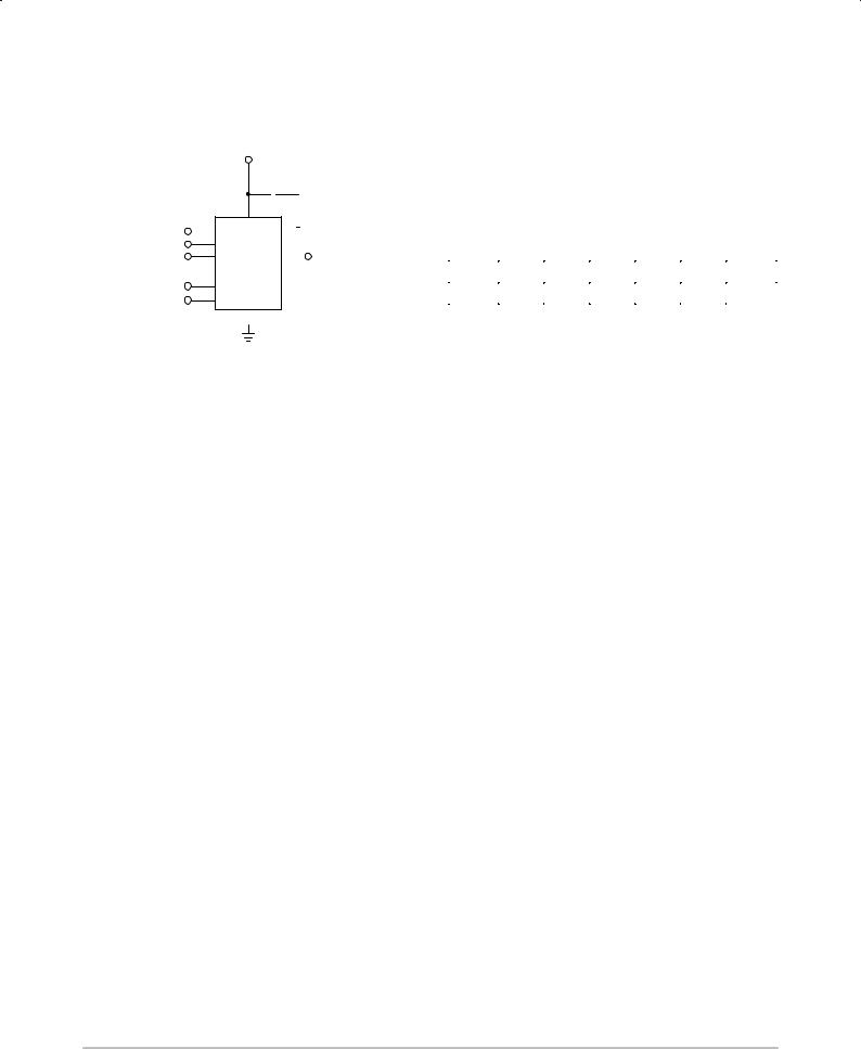
PIN DESCRIPTION
Pin No. |
Symbol |
Description |
|
|
|
1 |
SDA |
Bidirectional Serial Data |
|
|
|
2 |
SCL |
Serial Data Clock Input |
|
|
|
3 |
INT/CMPTR |
Interrupt or Comparator Output |
|
|
|
4 |
GND |
System Ground |
|
|
|
5 |
A2 |
Address Select Pin (MSB) |
6 |
A1 |
Address Select Pin |
7 |
A0 |
Address Select Pin (LSB) |
8 |
VDD |
Power Supply Input |
http://onsemi.com
2

LM75
ABSOLUTE MAXIMUM RATINGS*
Parameter |
Value |
Unit |
|
|
|
Supply Voltage (VDD) |
6.0 |
V |
ESD Susceptibility |
1000 |
V |
|
|
|
Input Voltage, On Pins: |
|
V |
A0, A1, A2 |
(GND ± 0.3) to (VCC + 0.3) |
|
SDA, SCL, INT/CMPTR |
(GND ± 0.3) to 5.5 |
|
|
|
|
Operating Temperature Range (TJ) |
±55 to +125 |
°C |
Storage Temperature Range (TSTG) |
±65 to +150 |
°C |
Lead Temperature Range (Soldering, 10 sec) |
+300 |
°C |
|
|
|
Thermal Resistance (Junction to Ambient) |
250 |
°C/W |
|
|
|
* Maximum Ratings are those values beyond which damage to the device may occur.
ELECTRICAL CHARACTERISTICS (Specifications Measured Over Operating Temperature Range, V+ = 5V, COSC = 0, Test Circuit (Figure 1), unless otherwise noted.
Symbol |
|
Characteristic |
|
|
Min |
Typ |
Max |
Unit |
|
|
|
|
|
|
|
|
|
|
|
V+H |
Supply Voltage Range, High |
|
|
|
|
|
|
V |
|
|
(±40°C ≤ TA ≤ +85°C, RL = 10 kW, LV Open) |
|
|
3.0 |
Ð |
10 |
|
||
V+L |
Supply Voltage Range, Low |
|
|
|
|
|
|
V |
|
|
(±40°C ≤ TA ≤ +85°C, RL = 10 kW, LV to GND) |
|
1.5 |
Ð |
3.5 |
|
|||
I+ |
Supply Current (RL = R) |
|
|
|
Ð |
80 |
180 |
μA |
|
ROUT |
Output Source Resistance |
|
|
|
|
|
|
W |
|
|
IOUT = 20mA, TA |
= 25°C |
|
|
|
Ð |
70 |
100 |
|
|
IOUT = 20mA, 0°C |
≤ TA ≤ +70°C |
|
|
|
Ð |
Ð |
120 |
|
|
IOUT = 20mA, ±40°C ≤ TA ≤ +85°C |
|
|
|
Ð |
Ð |
130 |
|
|
|
+ |
° ≤ |
TA |
≤ |
° |
Ð |
150 |
300 |
|
|
V =2V, IOUT = 3 mA, LV to GND, 0 C |
|
+70 C |
|
|
|
|
||
FOSC |
Oscillator Frequency (Pin 7 Open) |
|
|
|
Ð |
10 |
Ð |
kHz |
|
PEFF |
Power Efficiency (RL = 5kW) |
|
|
|
95 |
98 |
Ð |
% |
|
VOUT EFF |
Voltage Conversion Efficiency |
|
|
|
97 |
99.9 |
Ð |
% |
|
ZOSC |
Oscillator Impedance |
|
|
|
|
|
|
|
kW |
|
V+ = 2V |
|
|
|
|
Ð |
1000 |
Ð |
|
|
V+ = 5V |
|
|
|
|
Ð |
100 |
Ð |
|
http://onsemi.com
3
LM75
DETAILED OPERATING DESCRIPTION
A typical LM75 hardware connection is shown in Figure 1.
|
|
|
|
+V DD |
||||||||
|
|
|
|
C Bypass 0.1mF Recommended |
||||||||
|
|
|
|
|
|
|
|
|
|
Unless Device is |
||
|
|
|
|
|
|
|
|
|
|
|||
|
|
8 |
|
|
|
|
|
|
Mounted Close to CPU |
|||
Address |
A 0 |
7 |
|
|
|
|
|
|
|
|
|
|
|
|
|
|
|
|
|
|
|
|
|||
|
|
|
|
|
|
|
|
|
|
|||
6 |
|
|
|
|
|
|
|
|
|
|
||
(Set as Desired) A 1 |
5 |
|
3 |
|
|
|
|
|
||||
|
A 2 |
|
TCN75 |
|
|
|||||||
|
1 |
INT/CMPTR |
||||||||||
|
|
|
|
|
|
|||||||
Two Wire |
SDA |
|
|
|
|
|
|
|
|
|
|
|
2 |
|
|
|
|
|
|
|
|
|
|
||
Interface |
SCL |
|
|
|
|
|
|
|
|
|
|
|
|
|
|
|
|
|
|
|
|
|
|
||
|
|
4 |
|
|
|
|
|
|
|
|
|
|
|
|
|
|
|
|
|
|
|
|
|
||
|
|
|
|
|
|
|
|
|
|
|
|
|
Slave Address
The four most significant bits of the Address Byte (A6, A5, A4, A3) are fixed to 1001[B]. The states of A2, A1 and A0 in the serial bit stream must match the states of the A2, A1 and A0 address inputs for the LM75 to respond with an Acknowledge (indicating the LM75 is on the bus and ready to accept data). The Slave Address is represented by:
LM75 Slave Address
1 |
0 |
0 |
1 |
A2 |
A1 |
A0 |
|
|
|
|
|
|
|
MSB |
|
|
|
|
|
LSB |
|
|
|
|
|
|
|
Comparator/Interrupt Modes
Figure 1. Typical Application
Serial Data (SDA)
Bidirectional. Serial data is transferred in both directions using this pin.
Serial Clock (SCL)
Input. Clocks data into and out of the LM75.
INT/CMPTR
Open Collector, Programmable Polarity. In Comparator Mode, unconditionally driven active any time temperature exceeds the value programmed into the TSET register. INT/CMPTR will become inactive when temperature subsequently falls below the THYST setting. (See Register Set and Programmer's Model.) In Interrupt Mode, INT/CMPTR is made active by TEMP exceeding TSET; it is unconditionally reset to its inactive state by reading any register via the 2±wire bus. If and when temperature falls below THYST, INT/CMPTR is again driven active. Reading any register will clear the THYST interrupt. In Interrupt Mode, the INT/CMPTR output is unconditionally reset upon entering Shutdown Mode. If programmed as an active±low output, it can be wire±ORed with any number of other open collector devices. Most systems will require a pull±up resistor for this configuration.
Note that current sourced from the pull±up resistor causes power dissipation and may cause internal heating of the LM75. To avoid affecting the accuracy of ambient temperature readings, the pull±up resistor should be made as large as possible. INT/CMPTR's output polarity may be programmed by writing to the INT/CMPTR POLARITY bit in the CONFIG register. The default is active low.
Address (A2, A1, A0)
Inputs. Sets the three least significant bits of the LM75 8±bit address. A match between the LM75's address and the address specified in the serial bit stream must be made to initiate communication with the LM75. Many protocol±compatible devices with other addresses may share the same 2±wire bus.
INT/CMPTR behaves differently depending on whether the LM75 is in Comparator Mode or Interrupt Mode. Comparator Mode is designed for simple thermostatic operation. INT/CMPTR will go active anytime TEMP exceeds TSET. When in Comparator Mode, INT/CMPTR will remain active until TEMP falls below THYST, whereupon it will reset to its inactive state. The state of INT/CMPTR is maintained in shutdown mode when the LM75 is in comparator mode. In Interrupt Mode, INT/CMPTR will remain active indefinitely, even if TEMP falls below THYST, until any register is read via the 2±wire bus. Interrupt Mode is better suited to interrupt driven microprocessor±based systems. The INT/CMPTR output may be wire±OR'ed with other interrupt sources in such systems. Note that a pull±up resistor is necessary on this pin since it is an open±drain output. Entering Shutdown Mode will unconditionally reset INT/CMPTR when in Interrupt Mode.
SHUTDOWN MODE
When the appropriate bit is set in the configuration register (CONFIG) the LM75 enters its low±power shutdown mode (IDD = 1μA, typical) and the temperature±to±digital conversion process is halted. The LM75's bus interface remains active and TEMP, TSET, and THYST may be read from and written to. Transitions on SDA or SCL due to external bus activity may increase the standby power consumption. If the LM75 is in Interrupt Mode, the state of INT/CMPTR will be RESET upon entering shutdown mode.
Fault Queue
To lessen the probability of spurious activation of INT/CMPTR the LM75 may be programmed to filter out transient events. This is done by programming the desired value into the Fault Queue. Logic inside the LM75 will prevent the device from triggering INT/CMPTR unless the programmed number of sequential temperature±to±digital conversions yield the same qualitative result. In other words, the value reported in TEMP must remain above TSET or below THYST for the consecutive number of cycles
http://onsemi.com
4
 Loading...