


MOTOROLA LM317MBSTT1, LM317MBDTRK, LM317MBDT, LM317MADTRK, LM317MABT Datasheet
...LM317M
Three-Terminal Adjustable
Output Positive Voltage
Regulator
The LM317M is an adjustable three±terminal positive voltage regulator capable of supplying in excess of 500 mA over an output voltage range of 1.2 V to 37 V. This voltage regulator is exceptionally easy to use and requires only two external resistors to set the output voltage. Further, it employs internal current limiting, thermal shutdown and safe area compensation, making it essentially blow±out proof.
The LM317M serves a wide variety of applications including local, on±card regulation. This device also makes an especially simple adjustable switching regulator, a programmable output regulator, or by connecting a fixed resistor between the adjustment and output, the LM317M can be used as a precision current regulator.
•Output Current in Excess of 500 mA
•Output Adjustable between 1.2 V and 37 V
•Internal Thermal Overload Protection
•Internal Short Circuit Current Limiting
•Output Transistor Safe±Area Compensation
•Floating Operation for High Voltage Applications
•Eliminates Stocking Many Fixed Voltages
Simplified Application
Vin |
|
|
Vout |
Vout |
Vin |
LM317M |
|
||
|
|
|
R1 |
|
|
IAdj |
|
240 |
|
* |
Adjust |
+ |
** |
|
C |
|
|
C |
|
in |
|
|
|
O |
0.1μF |
|
|
|
1.0μF |
|
|
R2 |
|
|
*= Cin is required if regulator is located an appreciable distance from power supply filter.
**= CO is not needed for stability, however, it does improve transient response.
Vout + 1.25 V 1 ) R2 ) IAdj R2
R1
Since IAdj is controlled to less than 100 μA, the error associated with this term is negligible in most applications.
http://onsemi.com
Heatsink surface connected to Pin 2
1
2
|
3 |
|
|
TO±220AB |
|
|
T SUFFIX |
|
|
CASE 221A |
|
|
SOT±223 |
|
1 |
ST SUFFIX |
|
CASE 318E |
||
2 |
||
|
3 |
DPAK |
|
|
|
DT SUFFIX |
1 |
2 |
|
CASE 369A |
|||
|
|||
|
3 |
||
|
|
Heatsink Surface (shown as terminal 4 in case outline drawing) is connected to Pin 2.
|
PIN ASSIGNMENT |
|
|
1 |
Adjust |
|
|
2 |
Vout |
3 |
Vin |
|
|
ORDERING INFORMATION
See detailed ordering and shipping information in the package dimensions section on page 10 of this data sheet.
Semiconductor Components Industries, LLC, 1999 |
1 |
Publication Order Number: |
November, 1999 ± Rev. 6 |
|
LM317M/D |

LM317M
MAXIMUM RATINGS (TA = 25°C, unless otherwise noted.) |
|
|
|
|
|
|
|
|
|
||||
|
Rating |
|
Symbol |
|
|
Value |
|
Unit |
|
|
|
|
|
|
|
|
|
|
|
|
|
|
|
|
|
|
|
Input±Output Voltage Differential |
|
VI±VO |
|
40 |
|
Vdc |
|
|
|
|
|
||
Power Dissipation (Package Limitation) (Note 1) |
|
|
|
|
|
|
|
|
|
|
|
|
|
Plastic Package, T Suffix, Case 221A |
|
|
|
|
|
|
|
|
|
|
|
|
|
TA = 25°C |
|
PD |
|
Internally Limited |
|
|
|
|
|
|
|
||
Thermal Resistance, Junction±to±Air |
|
θJA |
|
70 |
|
°C/W |
|
|
|
|
|
||
Thermal Resistance, Junction±to±Case |
|
θJC |
|
5.0 |
|
°C/W |
|
|
|
|
|
||
Plastic Package, DT Suffix, Case 369A |
|
|
|
|
|
|
|
|
|
|
|
|
|
TA = 25°C |
|
PD |
|
Internally Limited |
|
|
|
|
|
|
|
||
Thermal Resistance, Junction±to±Air |
|
θJA |
|
92 |
|
°C/W |
|
|
|
|
|
||
Thermal Resistance, Junction±to±Case |
|
θJC |
|
5.0 |
|
°C/W |
|
|
|
|
|
||
Plastic Package, ST Suffix, Case 318E |
|
|
|
|
|
|
|
|
|
|
|
|
|
TA = 25°C |
|
PD |
|
Internally Limited |
|
|
|
|
|
|
|
||
Thermal Resistance, Junction±to±Air |
|
θJA |
|
245 |
|
°C/W |
|
|
|
|
|
||
Thermal Resistance, Junction±to±Case |
|
θJC |
|
15 |
|
°C/W |
|
|
|
|
|
||
Operating Junction Temperature Range |
|
TJ |
|
± 40 to +125 |
|
°C |
|
|
|
|
|
||
Storage Temperature Range |
|
Tstg |
|
± 65 to +150 |
|
°C |
|
|
|
|
|
||
NOTE: 1. Figure 23 provides thermal resistance versus pc board pad size. |
|
|
|
|
|
|
|
|
|
||||
ELECTRICAL CHARACTERISTICS (VI±VO = 5.0 V; IO = 0.1 A, TJ = Tlow to Thigh [Note 1], unless otherwise noted.) |
|
||||||||||||
|
Characteristics |
|
|
|
|
Figure |
Symbol |
|
Min |
Typ |
Max |
Unit |
|
|
|
|
|
|
|
|
|
|
|
|
|||
Line Regulation (Note 2) |
|
|
|
|
1 |
Regline |
± |
0.01 |
0.04 |
%/V |
|||
TA = 25°C, 3.0 V ≤ VI±VO ≤ 40 V |
|
|
|
|
|
|
|
|
|
|
|
|
|
Load Regulation (Note 2) |
|
|
|
|
2 |
Regload |
|
|
|
|
|
||
TA = 25°C, 10 mA ≤ IO ≤ 0.5 A |
|
|
|
|
|
|
|
|
|
|
|
|
|
VO |
≤ 5.0 V |
|
|
|
|
|
|
|
± |
5.0 |
25 |
mV |
|
VO |
≥ 5.0 V |
|
|
|
|
|
|
|
± |
0.1 |
0.5 |
% VO |
|
Adjustment Pin Current |
|
|
|
|
3 |
|
IAdj |
± |
50 |
100 |
μA |
||
Adjustment Pin Current Change |
|
|
|
|
1,2 |
|
IAdj |
± |
0.2 |
5.0 |
μA |
||
2.5 V ≤ VI±VO ≤ 40 V, 10 mA ≤ IL ≤ 0.5 A, PD ≤ Pmax |
|
|
|
|
|
|
|
|
|
||||
Reference Voltage |
|
|
|
|
3 |
|
Vref |
|
|
|
|
V |
|
3.0 V ≤ VI±VO ≤ 40 V, 10 mA ≤ IO ≤ 0.5 A, PD ≤ Pmax: |
|
|
|
|
1.200 |
1.250 |
1.300 |
|
|||||
Line Regulation (Note 2) |
|
|
|
|
1 |
Regline |
± |
0.02 |
0.07 |
%/V |
|||
3.0 V ≤ VI±VO ≤ 40 V |
|
|
|
|
|
|
|
|
|
|
|
|
|
Load Regulation (Note 2) |
|
|
|
|
2 |
Regload |
|
|
|
|
|
||
10 mA ≤ IO ≤ 0.5 A |
|
|
|
|
|
|
|
|
|
|
|
|
|
VO |
≤ 5.0 V |
|
|
|
|
|
|
|
± |
20 |
70 |
mV |
|
VO |
≥ 5.0 V |
|
|
|
|
|
|
|
± |
0.3 |
1.5 |
% VO |
|
Temperature Stability (Tlow ≤ TJ ≤ Thigh) |
|
|
|
|
3 |
|
TS |
± |
0.7 |
± |
% VO |
||
Minimum Load Current to Maintain Regulation |
|
|
|
|
3 |
|
ILmin |
± |
3.5 |
10 |
mA |
||
(VI±VO = 40 V) |
|
|
|
|
|
|
|
|
|
|
|
|
|
Maximum Output Current |
|
|
|
|
3 |
|
Imax |
|
|
|
|
A |
|
VI±VO ≤ 15 V, PD ≤ Pmax |
|
|
|
|
|
|
|
0.5 |
0.9 |
± |
|
||
VI±VO = 40 V, PD ≤ Pmax, TA = 25°C |
|
|
|
|
|
|
|
0.15 |
0.25 |
± |
|
||
RMS Noise, % of VO |
|
|
|
|
± |
|
N |
± |
0.003 |
± |
% VO |
||
TA= 25°C, 10 Hz ≤ f ≤ 10 kHz |
|
|
|
|
|
|
|
|
|
|
|
|
|
Ripple Rejection, VO = 10 V, f = 120 Hz (Note 3) |
|
|
|
|
4 |
|
RR |
|
|
|
|
dB |
|
Without CAdj |
|
|
|
|
|
|
|
± |
65 |
± |
|
||
CAdj = 10 μF |
|
|
|
|
|
|
|
66 |
80 |
± |
|
||
Long±Term Stability, TJ = Thigh (Note 4) |
|
|
|
|
3 |
|
S |
± |
0.3 |
1.0 |
%/1.0 k |
||
TA= 25°C for Endpoint Measurements |
|
|
|
|
|
|
|
|
|
|
|
Hrs. |
|
NOTES: 1. Tlow to Thigh = 0° to +125°C for LM317M |
Tlow to Thigh = ± 40° to +125°C for LM317MB |
|
|
|
|
|
|||||||
2.Load and line regulation are specified at constant junction temperature. Changes in VO due to heating effects must be taken into account separately. Pulse testing with low duty cycle is used.
3.CAdj, when used, is connected between the adjustment pin and ground.
4.Since Long±Term Stability cannot be measured on each device before shipment, this specification is an engineering estimate of average stability from lot to lot.
http://onsemi.com
2

LM317M
Representative Schematic Diagram
Vin |
|
|
|
|
|
|
|
300 |
300 |
|
300 |
3.0k |
300 |
70 |
6.8V |
|
|
|
|
|
|
|
6.8V |
350 |
|
|
|
|
|
|
|
|
|
|
|
|
|
|
18k |
|
|
8.67k |
|
|
|
|
500 |
|
130 |
|
|
|
|
|
|
|
|
|
|
|
|
|
|
|
|
|
|
5.1k |
|
|
400 |
200k |
|
|
|
|
|
|
|
|
|
|
|
|
|
|
|
180 |
180 |
2.0k |
6.0k |
10 |
|
60 |
1.25 |
6.3V |
|
|
|
pF |
10 |
|
|
|
|
|
|
|
|
||
|
|
|
|
|
|
|
|
|
|
|
|
|
pF |
|
|
 Vout
Vout
2.4k
12.8k 50
 Adjust
http://onsemi.com
3
LM317M
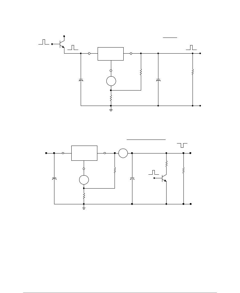
Figure 1. Line Regulation and |
IAdj/Line Test Circuit |
|
|||||
VCC |
|
|
|
|
|
VOH ± VOL |
|
|
|
|
Line Regulation (%/V) = |
x 100 |
|||
* |
|
|
VOL |
||||
|
|
|
|
|
|
||
VIH |
|
|
Vout |
|
|
|
VOH |
VIL |
Vin |
LM317M |
|
|
|
VOL |
|
|
|
|
|
|
|
|
|
|
|
Adjust |
R1 |
240 |
|
|
RL |
|
|
|
1% |
+ |
|
||
|
|
|
|
|
|
||
|
0.1μF |
|
|
|
1.0μF |
|
|
Cin |
IAdj |
|
|
CO |
|
||
* Pulse Testing Required: |
|
R2 |
|
|
|
|
|
|
|
|
|
|
|
|
|
1% Duty Cycle is suggested. |
1% |
|
Figure 2. Load Regulation and IAdj/Load Test Circuit
Vin Vin
Cin 0.1μF
* Pulse Testing Required:
1% Duty Cycle is suggested.
|
Load Regulation (mV) = VO (min Load) ±VO (max Load) |
|
|
|
VO (min Load) ± VO (max Load) |
X 100 |
|
|
Load Regulation (% VO) = |
VO (min Load) |
|
|
|
VO (min Load) |
|
|
Vout |
|
VO (max Load) |
LM317M |
|
|
|
IL |
|
|
|
|
|
|
RL |
|
240 |
|
(max Load) |
Adjust |
|
RL |
|
R1 1% |
* |
||
|
|
+ |
(min Load) |
|
|
|
|
IAdj |
CO |
1.0μF |
|
R2 |
|
|
|
1% |
|
|
|
http://onsemi.com
4
 Loading...