


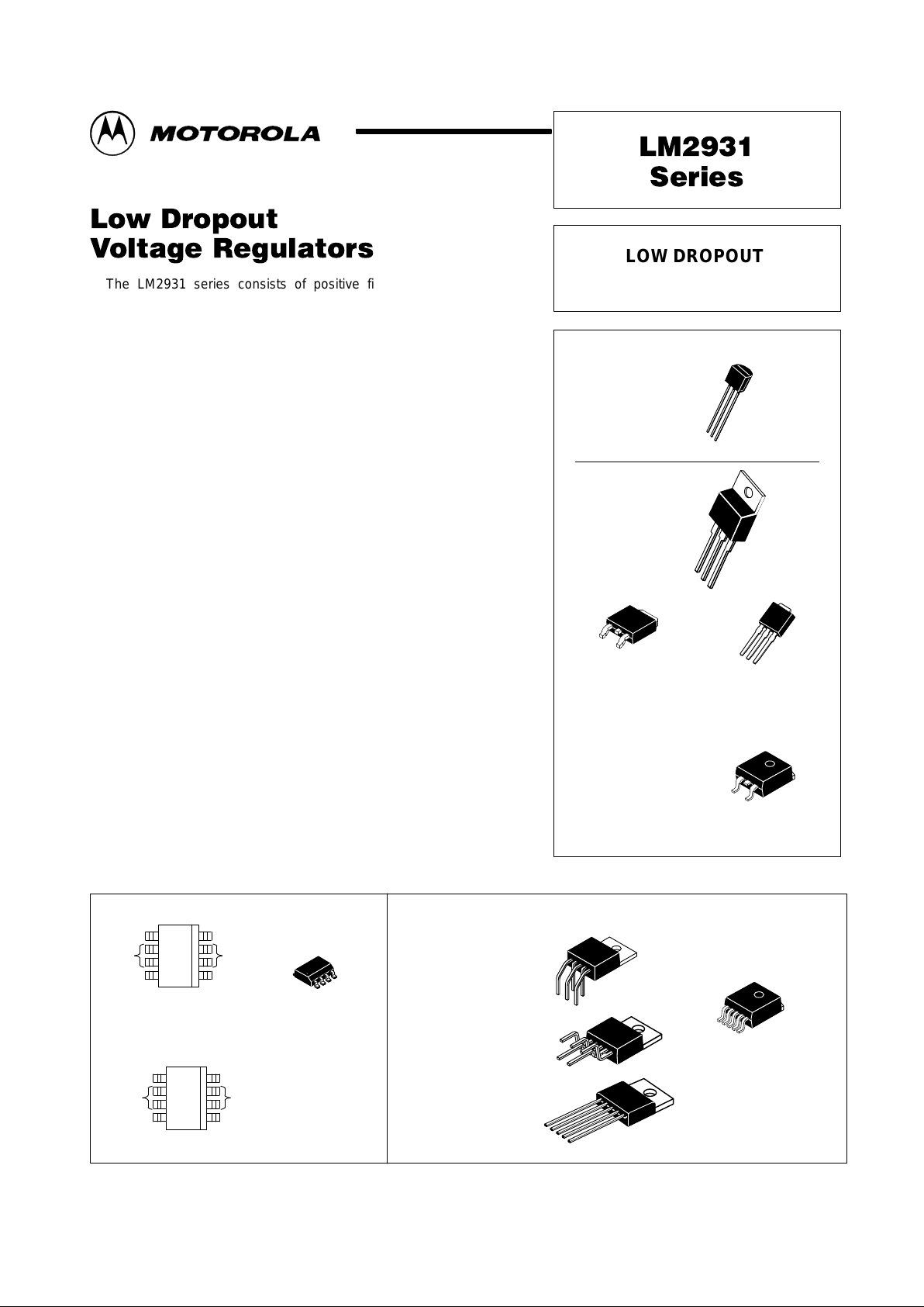
LM2931T
Motorola LM2931T, LM2931D2T, LM2931D, LM2931AZ, LM2931CD Datasheet
...
Order this document by LM2931/D
LOW DROPOUT
VOLTAGE REGULATORS
Z SUFFIX
PLASTIC PACKAGE
CASE 29
T SUFFIX
PLASTIC PACKAGE
CASE 221A
Heatsink surface
connected to Pin 2.
DT–1 SUFFIX
PLASTIC PACKAGE
CASE 369
(DPAK)
D2T SUFFIX
PLASTIC PACKAGE
CASE 936
(D2PAK)
Pin 1. Output
2. Ground
3. Input
Pin 1. Input
2. Ground
3. Output
Heatsink surface (shown as terminal 4 in
case outline drawing) is connected to Pin 2.
3
1
2
DT SUFFIX
PLASTIC PACKAGE
CASE 369A
(DPAK)
3
1
2
FIXED OUTPUT VOLTAGE
3
1
2
3
1
2
3
1
1
MOTOROLA ANALOG IC DEVICE DATA
The LM2931 series consists of positive fixed and adjustable output
voltage regulators that are specifically designed to maintain proper
regulation with an extremely low input–to–output voltage differential. These
devices are capable of supplying output currents in excess of 100 mA and
feature a low bias current of 0.4 mA at 10 mA output.
Designed primarily to survive in the harsh automotive environment, these
devices will protect all external load circuitry from input fault conditions
caused by reverse battery connection, two battery jump starts, and
excessive line transients during load dump. This series also includes internal
current limiting, thermal shutdown, and additionally, is able to withstand
temporary power–up with mirror–image insertion.
Due to the low dropout voltage and bias current specifications, the
LM2931 series is ideally suited for battery powered industrial and consumer
equipment where an extension of useful battery life is desirable. The ‘C’
suffix adjustable output regulators feature an output inhibit pin which is
extremely useful in microprocessor–based systems.
• Input–to–Output Voltage Differential of < 0.6 V @ 100 mA
• Output Current in Excess of 100 mA
• Low Bias Current
• 60 V Load Dump Protection
• –50 V Reverse Transient Protection
• Internal Current Limiting with Thermal Shutdown
• Temporary Mirror–Image Protection
• Ideally Suited for Battery Powered Equipment
• Economical 5–Lead TO–220 Package with Two Optional Leadforms
• Available in Surface Mount SOP–8, D
2
PAK and DPAK Packages
• High Accuracy (±2%) Reference (LM2931AC) Available
D SUFFIX
PLASTIC PACKAGE
CASE 751
(SOP–8)
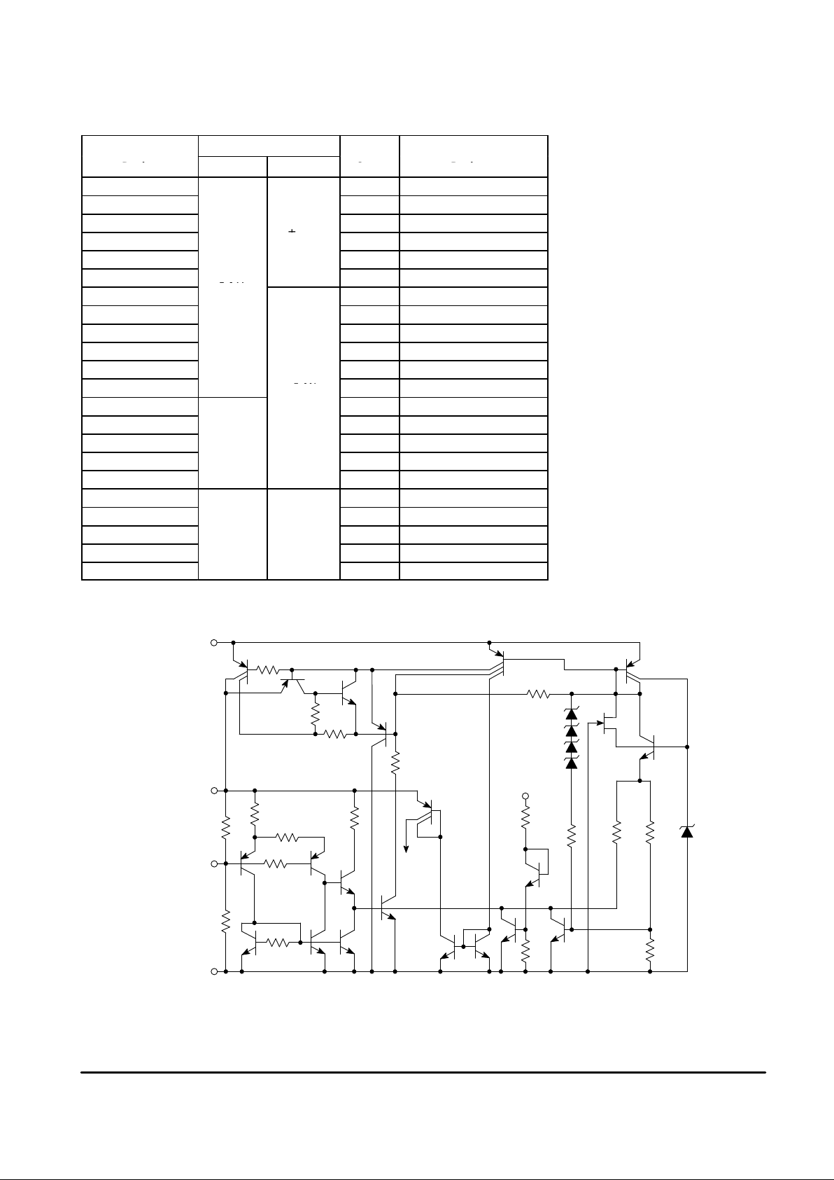
1
8
ADJUSTABLE
FIXED
(Top View)
N.C.
Gnd
Input
N.C.
Gnd
Output18
54
(Top View)
Output
Inhibit
Gnd
Input
Adjust
Gnd
Output18
54
TV SUFFIX
PLASTIC PACKAGE
CASE 314B
T SUFFIX
PLASTC PACKAGE
CASE 314D
TH SUFFIX
PLASTIC PACKAGE
CASE 314A
D2T SUFFIX
PLASTIC PACKAGE
CASE 936A
(D2PAK)
Heatsink surface connected to Pin 3.
Pin 1. Adjust
2. Output Inhibit
3. Ground
4. Input
5. Output
Heatsink surface (shown as
terminal 6 in case outline
drawing) is connected to Pin 3.
5
1
5
1
5
1
5
1
ADJUSTABLE OUTPUT VOLTAGE
(See Following Page for Ordering Information.)
Motorola, Inc. 1997 Rev 4
LM2931 Series
2
MOTOROLA ANALOG IC DEVICE DATA
ORDERING INFORMATION
Output
Device
Voltage Tolerance
Case Package
LM2931AD–5.0
751 SOP–8 Surface Mount
LM2931ADT–5.0
369A Surface Mount DPAK
LM2931ADT–1–5.0
369 DPAK
LM2931AD2T–5.0
±3.8%
936 Surface Mount D2PAK
LM2931A T–5.0
221A TO–220 Type
LM2931AZ–5.0
29 TO–92 Type
LM2931D–5.0
5.0 V
751 SOP–8 Surface Mount
LM2931D2T–5.0
936 Surface Mount D2PAK
LM2931DT–5.0
369A Surface Mount DPAK
LM2931DT–1–5.0
369 DPAK
LM2931T–5.0
221A TO–220 Type
LM2931Z–5.0
±5.0%
29 TO–92 Type
LM2931CD
751 SOP–8 Surface Mount
LM2931CD2T
936A Surface Mount D2PAK
LM2931CT
Adjustable
314D 5–Pin TO–220 Type
LM2931CTH
j
314A 5–Pin Horizontal Leadform
LM2931CTV 314B 5–Pin Vertical Leadform
LM2931ACD
751 SOP–8 Surface Mount
LM2931ACD2T
936A Surface Mount D2PAK
LM2931ACT
Adjustable ±2.0%
314D 5–Pin TO–220 Type
LM2931ACTH 314A 5–Pin Horizontal Leadform
LM2931ACTV 314B 5–Pin Vertical Leadform
Representative Schematic Diagram
*Deleted on Adjustable Regulators
Input
Output
30 k *
Adjust
92.8 k *
Ground
350
500
6.0 k
6.0
30 k
Output
Inhibit
EPI
Bias
50 k
5.8 V
10 k
11.5 k
3.0 k
3.94 k
30 k
30 k
180 k 184 k
6.8 V
35 k
48 k
This device contains 26 active transistors.
LM2931 Series
3
MOTOROLA ANALOG IC DEVICE DATA
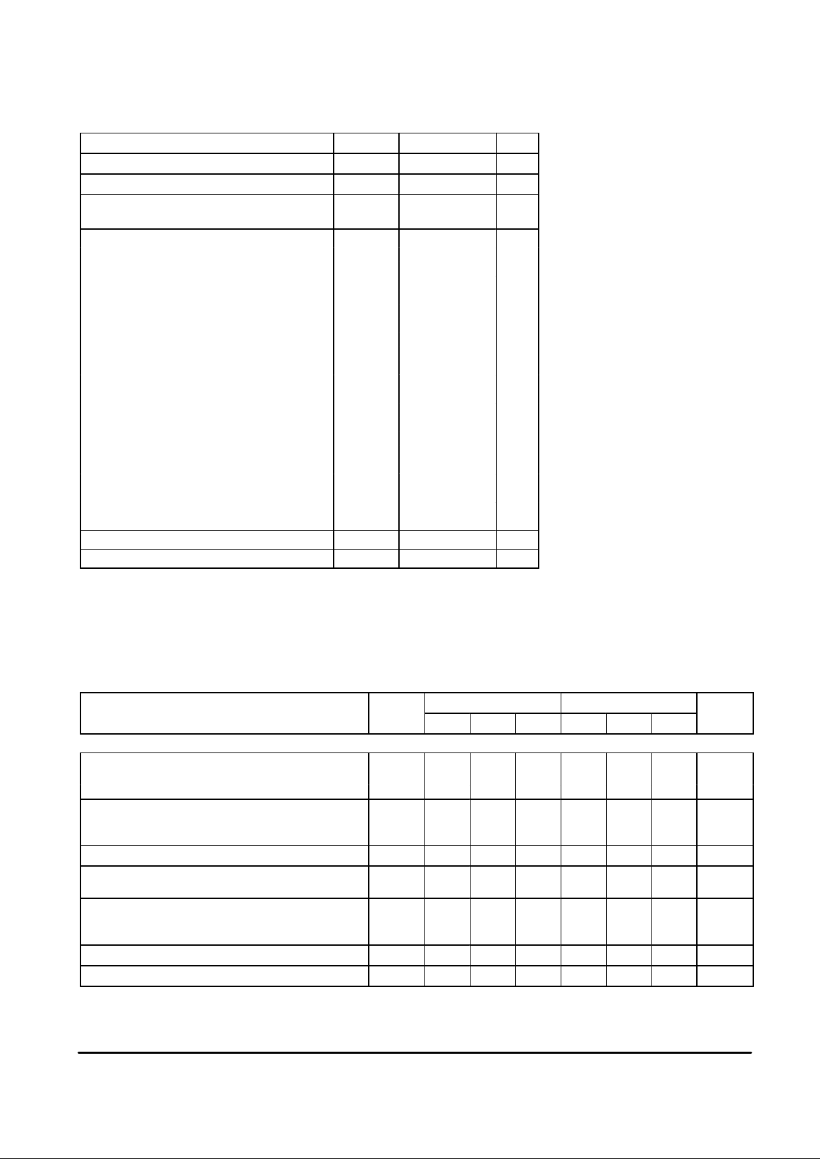
MAXIMUM RATINGS
Rating Symbol Value Unit
Input Voltage Continuous V
I
40 Vdc
Transient Input V oltage (τ ≤100 ms) VI(τ) 60 Vpk
Transient Reverse Polarity Input V oltage –VI(τ) –50– Vpk
1.0% Duty Cycle, τ ≤ 100 ms
Power Dissipation
Case 29 (TO–92 Type)
TA = 25°C P
D
Internally Limited W
Thermal Resistance, Junction–to–Ambient R
θJA
178 °C/W
Thermal Resistance, Junction–to–Case R
θJC
83 °C/W
Case 221A, 314A, 314B and 314D (TO–220 Type)
TA = 25°C P
D
Internally Limited W
Thermal Resistance, Junction–to–Ambient R
θJA
65 °C/W
Thermal Resistance, Junction–to–Case R
θJC
5.0 °C/W
Case 369 and 369A (DPAK) [Note 1]
TA = 25°C P
D
Internally Limited W
Thermal Resistance, Junction–to–Ambient R
θJA
92 °C/W
Thermal Resistance, Junction–to–Case R
θJC
6.0 °C/W
Case 751 (SOP–8) [Note 2]
TA = 25°C P
D
Internally Limited W
Thermal Resistance, Junction–to–Ambient R
θJA
160 °C/W
Thermal Resistance, Junction–to–Case R
θJC
25 °C/W
Case 936 and 936A (D2PAK) [Note 3]
TA = 25°C P
D
Internally Limited W
Thermal Resistance, Junction–to–Ambient R
θJA
70 °C/W
Thermal Resistance, Junction–to–Case R
θJC
5.0 °C/W
Tested Operating Junction Temperature Range T
J
–40 to +125 °C
Storage Temperature Range T
stg
–65 to +150 °C
NOTES: 1. DPAK Junction–to–Ambient Thermal Resistance is for vertical mounting. Refer to Figure 24 for
board mounted Thermal Resistance.
2.SOP–8 Junction–to–Ambient Thermal Resistance is for minimum recommended pad size. Refer
to Figure 23 for Thermal Resistance variation versus pad size.
3.D2PAK Junction–to–Ambient Thermal Resistance is for vertical mounting. Refer to Figure 25 for
board mounted Thermal Resistance.
4.ESD data available upon request.
ELECTRICAL CHARACTERISTICS (V
in
= 14 V, IO = 10 mA, CO = 100 µF, C
O(ESR)
= 0.3 Ω, TJ = 25°C [Note 1].)
LM2931–5.0 LM2931A–5.0
Characteristic Symbol
Min Typ Max Min Typ Max
Unit
FIXED OUTPUT
Output Voltage V
O
V
Vin = 14 V, IO = 10 mA, TJ = 25°C 4.75 5.0 5.25 4.81 5.0 5.19
Vin = 6.0 V to 26 V, IO ≤ 100 mA, TJ = –40° to +125°C 4.50 – 5.50 4.75 – 5.25
Line Regulation Reg
line
mV
Vin = 9.0 V to 16 V – 2.0 10 – 2.0 10
Vin = 6.0 V to 26 V – 4.0 30 – 4.0 30
Load Regulation (IO = 5.0 mA to 100 mA) Reg
load
– 14 50 – 14 50 mV
Output Impedance Z
O
mΩ
IO = 10 mA, ∆IO = 1.0 mA, f = 100 Hz to 10 kHz – 200 – – 200 –
Bias Current I
B
mA
Vin = 14 V, IO = 100 mA, TJ = 25°C – 5.8 30 – 5.8 30
Vin = 6.0 V to 26 V, IO = 10 mA, TJ = –40° to +125°C – 0.4 1.0 – 0.4 1.0
Output Noise Voltage (f = 10 Hz to 100 kHz) V
n
– 700 – – 700 – µVrms
Long Term Stability S – 20 – – 20 – mV/kHR
NOTES: 1. Low duty cycle pulse techniques are used during test to maintain junction temperature as close to ambient as possible.
2.The reference voltage on the adjustable device is measured from the output to the adjust pin across R1.
LM2931 Series
4
MOTOROLA ANALOG IC DEVICE DATA
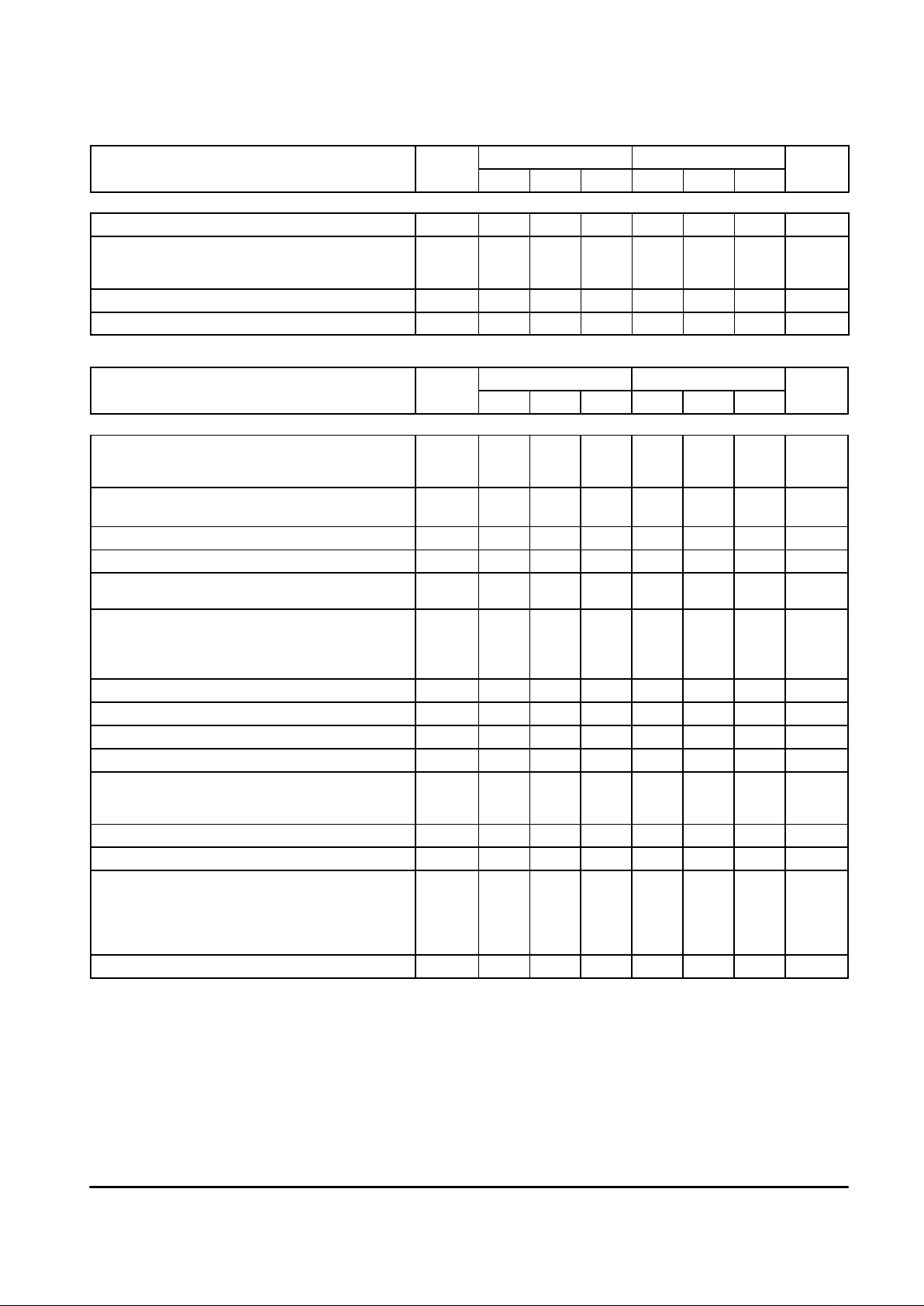
ELECTRICAL CHARACTERISTICS
(Vin = 14 V, IO = 10 mA, CO = 100 µF, C
O(ESR)
= 0.3 Ω, TJ = 25°C [Note 1].)
LM2931–5.0 LM2931A–5.0
Characteristic Symbol
Min Typ Max Min Typ Max
Unit
FIXED OUTPUT
Ripple Rejection (f = 120 Hz) RR 60 90 – 60 90 – dB
Dropout Voltage VI–V
O
V
IO = 10 mA – 0.015 0.2 – 0.015 0.2
IO = 100 mA – 0.16 0.6 – 0.16 0.6
Over–Voltage Shutdown Threshold V
th(OV)
26 29.5 40 26 29.5 40 V
Output Voltage with Reverse Polarity Input (Vin = –15 V) –V
O
–0.3 0 – –0.3 0 – V
ELECTRICAL CHARACTERISTICS (V
in
= 14 V, IO = 10 mA, CO = 100 µF, C
O(ESR)
= 0.3 Ω, TJ = 25°C [Note 1].)
LM2931C LM2931AC
Characteristic Symbol Min Typ Max Min Typ Typ Unit
ADJUSTABLE OUTPUT
Reference Voltage (Note 2, Figure 18) V
ref
V
IO = 10 mA, TJ = 25°C 1.14 1.20 1.26 1.17 1.20 1.23
IO ≤ 100 mA, TJ = –40 to +125°C 1.08 – 1.32 1.15 – 1.25
Output Voltage Range VO
range
3.0 to242.7 to
29.5
– 3.0 to242.7 to
29.5
– V
Line Regulation (Vin = VO + 0.6 V to 26 V) Reg
line
– 0.2 1.5 – 0.2 1.5 mV/V
Load Regulation (IO = 5.0 mA to 100 mA) Reg
load
– 0.3 1.0 – 0.3 1.0 %/V
Output Impedance Z
O
mΩ/V
IO = 10 mA, ∆IO = 1.0 mA, f = 10 Hz to 10 kHz – 40 – – 40 –
Bias Current I
B
mA
IO = 100 mA – 6.0 – – 6.0 –
IO = 10 mA – 0.4 1.0 – 0.4 1.0
Output Inhibited (V
th(OI)
= 2.5 V) – 0.2 1.0 – 0.2 1.0
Adjustment Pin Current I
Adj
– 0.2 – – 0.2 – µA
Output Noise Voltage (f = 10 Hz to 100 kHz) V
n
– 140 – – 140 – µVrms/V
Long–Term Stability S – 0.4 – – 0.4 – %/kHR
Ripple Rejection (f = 120 Hz) RR 0.10 0.003 – 0.10 0.003 – %/V
Dropout Voltage VI–V
O
V
IO = 10 mA – 0.015 0.2 – 0.015 0.2
IO = 100 mA – 0.16 0.6 – 0.16 0.6
Over–Voltage Shutdown Threshold V
th(OV)
26 29.5 40 26 29.5 40 V
Output Voltage with Reverse Polarity Input (Vin = –15 V) –V
O
–0.3 0 – –0.3 0 – V
Output Inhibit Threshold Voltages V
th(OI)
V
Output “On”: TJ = 25°C – 2.15 1.90 – 2.15 1.90
TJ = –40° to +125°C – – 1.20 – – 1.20
Output “Off”: TJ = 25°C 2.50 2.26 – 2.50 2.26 –
TJ = –40° to +125°C 3.25 – – 3.25 – –
Output Inhibit Threshold Current (V
th(OI)
= 2.5 V) I
th(OI)
– 30 50 – 30 50 µA
NOTES: 1. Low duty cycle pulse techniques are used during test to maintain junction temperature as close to ambient as possible.
2.The reference voltage on the adjustable device is measured from the output to the adjust pin across R1.
LM2931 Series
5
MOTOROLA ANALOG IC DEVICE DATA
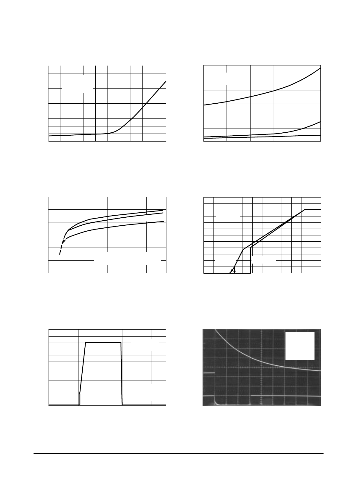
IO = 100 mA
IO = 10 mA
, OUTPUT VOL TAGE (V)
O
V
–V
in O
, DROPOUT VOLTAGE (mV)V
Vin, INPUT VOLTAGE (V)
–20 –10 0 10 20 30 40 50 60
0
1.0
2.0
3.0
4.0
5.0
6.0
V
out
= 5.0 V
RL = 500
Ω
TA = 25°C
, OUTPUT CURRENT (mA)
O
Vin, INPUT VOLTAGE (V)
50
150
250
350
0 5.0 10 15 20 25 30
I
TJ = –40°C
TJ = 25°C
TJ = 85°C
V
in
(10 V/DIV)
V
O
(5.0 V/DIV)
0
0
t, TIME (50 ms/DIV)
, INPUT VOLTAGE, OUTPUT VOL TAGE
, OUTPUT VOL TAGE (V)
O
Vin, INPUT VOLTAGE (V)
0
1.0
2.0
3.0
4.0
5.0
6.0
0 1.0 2.0 3.0 4.0 5.0 6.0
V
TJ, JUNCTION TEMPERATURE (°C)
0
100
200
300
0 25 50 75 100 125
IO = 50 mA
–V
in O
IO, OUTPUT CURRENT (mA)
0 20 40 60 80 100
0
40
80
120
160
200
Vin = 14 V
∆
V
out
= 100 mV
TJ = 25
°
C
, DROPOUT VOLTAGE (mV)V
V
out
= 5.0 V
RL = 50
Ω
CO = 100 µF
τ
= 150 ms
TA = 25
°
C
VCC = 15 V
V
FB1
= 5.05 V
Dashed lines below Vin = 5.0 V
are for Adjustable output devices only.
Figure 1. Dropout Voltage versus Output Current
Figure 2. Dropout Voltage versus
Junction Temperature
Figure 3. Peak Output Current versus Input Voltage Figure 4. Output Voltage versus Input Voltage
Figure 5. Output Voltage versus Input Voltage Figure 6. Load Dump Characteristics
Vin = 14 V
∆
V
out
= 100 mV
V
out
= 5.0 V
TA = 25
°
C
RL = 50
Ω
IO = 100 mA
 Loading...