


MOTOROLA LP2951CDMR2, LP2951CP1-005, LP2951CN-3.3, LP2951CN-3.0, LP2951CN Datasheet
...LP2950
Micropower Voltage Regulators
The LP2950 and LP2951 are micropower voltage regulators that are specifically designed to maintain proper regulation with an extremely low input±to±output voltage differential. These devices feature a very low quiescent bias current of 75 μA and are capable of supplying output currents in excess of 100 mA. Internal current and thermal limiting protection is provided.
The LP2951 has three additional features. The first is the Error Output that can be used to signal external circuitry of an out of regulation condition, or as a microprocessor power±on reset. The second feature allows the output voltage to be preset to 5.0 V, 3.3 V or 3.0 V output (depending on the version) or programmed from 1.25 V to 29 V. It consists of a pinned out resistor divider along with direct access to the Error Amplifier feedback input. The third feature is a Shutdown input that allows a logic level signal to turn±off or turn±on the regulator output.
Due to the low input±to±output voltage differential and bias current specifications, these devices are ideally suited for battery powered computer, consumer, and industrial equipment where an extension of useful battery life is desirable. The LP2950 is available in the three pin case 29 and DPAK packages, and the LP2951 is available in the eight pin dual±in±line, SO±8 and Micro±8 surface mount packages. The `A' suffix devices feature an initial output voltage tolerance
± 0.5%.
LP2950 and LP2951 Features:
•Low Quiescent Bias Current of 75 μA
•Low Input±to±Output Voltage Differential of 50 mV at 100 μA and 380 mV at 100 mA
•5.0 V, 3.3 V or 3.0 V ± 0.5% Allows Use as a Regulator or Reference
•Extremely Tight Line and Load Regulation
•Requires Only a 1.0 μF Output Capacitor for Stability
•Internal Current and Thermal Limiting
LP2951 Additional Features:
•Error Output Signals an Out of Regulation Condition
•Output Programmable from 1.25 V to 29 V
•Logic Level Shutdown Input
(See Following Page for Device Information.)
http://onsemi.com
TO±92 |
|
|
|
Z SUFFIX |
Pin: 1. |
Output |
|
CASE 29 |
|
2. |
Ground |
1 |
|
3. |
Input |
2 |
3 |
|
|
|
|
|
|
DPAK |
|
|
|
DT SUFFIX |
1 |
|
|
CASE 369A |
3 |
|
|
PIN CONNECTIONS |
|
||
|
Pin: 1. |
Input |
|
|
2. |
Ground |
|
1 2 3 |
3. |
Output |
|
(Top View)
Heatsink surface (shown as terminal 4 in case outline drawing) is connected to Pin 2.
SO±8 |
|
|
|
D SUFFIX |
8 |
|
|
CASE 751 |
|
1 |
|
|
|
|
|
N SUFFIX |
|
|
|
CASE 626 |
8 |
|
|
|
|
|
|
|
|
|
1 |
Micro±8 |
|
8 |
|
DM SUFFIX |
|
||
|
|
||
CASE 846A |
|
1 |
|
PIN CONNECTIONS |
|||
Output |
1 |
8 |
Input |
Sense |
2 |
7 |
Feedback |
Shutdown |
3 |
6 |
VO Tap |
|
|
|
|
Gnd |
4 |
5 |
Error Output |
(Top View)
ORDERING INFORMATION
See detailed ordering and shipping information in the package dimensions section on page 13 of this data sheet.
Semiconductor Components Industries, LLC, 1999 |
1 |
Publication Order Number: |
October, 1999 ± Rev. 5 |
|
LP2950/D |
LP2950
DEVICE INFORMATION
|
|
Output Voltage |
|
Operating Junction |
||
|
|
|
|
|
||
Package |
3.0V |
3.3V |
5.0V |
Adjustable |
Temperature Range |
|
|
|
|
|
|
|
|
TO±92 |
LP2950CZ±3.0 |
LP2950CZ±3.3 |
LP2950CZ±5.0 |
Not |
TJ = ±40° to +125°C |
|
Suffix Z |
LP2950ACZ±3.0 |
LP2950ACZ±3.3 |
LP2950ACZ±5.0 |
Available |
||
|
||||||
|
|
|
|
|
|
|
DPAK |
LP2950CDT±3.0 |
LP2950CDT±3.3 |
LP2950CDT±5.0 |
Not |
TJ = ±40° to +125°C |
|
Suffix DT |
LP2950ACDT±3.0 |
LP2950ACDT±3.3 |
LP2950ACDT±5.0 |
Available |
||
|
||||||
|
|
|
|
|
|
|
SO±8 |
LP2951CD±3.0 |
LP2951CD±3.3 |
LP2951CD |
LP2951CD |
TJ = ±40° to +125°C |
|
Suffix D |
LP2951ACD±3.0 |
LP2951ACD±3.3 |
LP2951ACD |
LP2951ACD |
||
|
||||||
|
|
|
|
|
|
|
Micro±8 |
LP2951CDM±3.0 |
LP2951CDM±3.3 |
LP2951CDM |
LP2951CDM |
TJ = ±40° to +125°C |
|
Suffix DM |
LP2951ACDM±3.0 |
LP2951ACDM±3.3 |
LP2951ACDM |
LP2951ACDM |
||
|
||||||
|
|
|
|
|
|
|
DIP±8 |
LP2951CN±3.0 |
LP2951CN±3.3 |
LP2951CN |
LP2951CN |
TJ = ±40° to +125°C |
|
Suffix N |
LP2951ACN±3.0 |
LP2951ACN±3.3 |
LP2951ACN |
LP2951ACN |
||
|
||||||
|
|
|
|
|
|
|
LP2950Cx±xx / LP2951Cxx±xx |
1% Output Voltage Precision at TJ = 25°C |
|
|
|||
LP2950ACx±xx / LP2951ACxx±xx |
0.5% Output Voltage Precision at TJ = 25°C |
|
|
|||
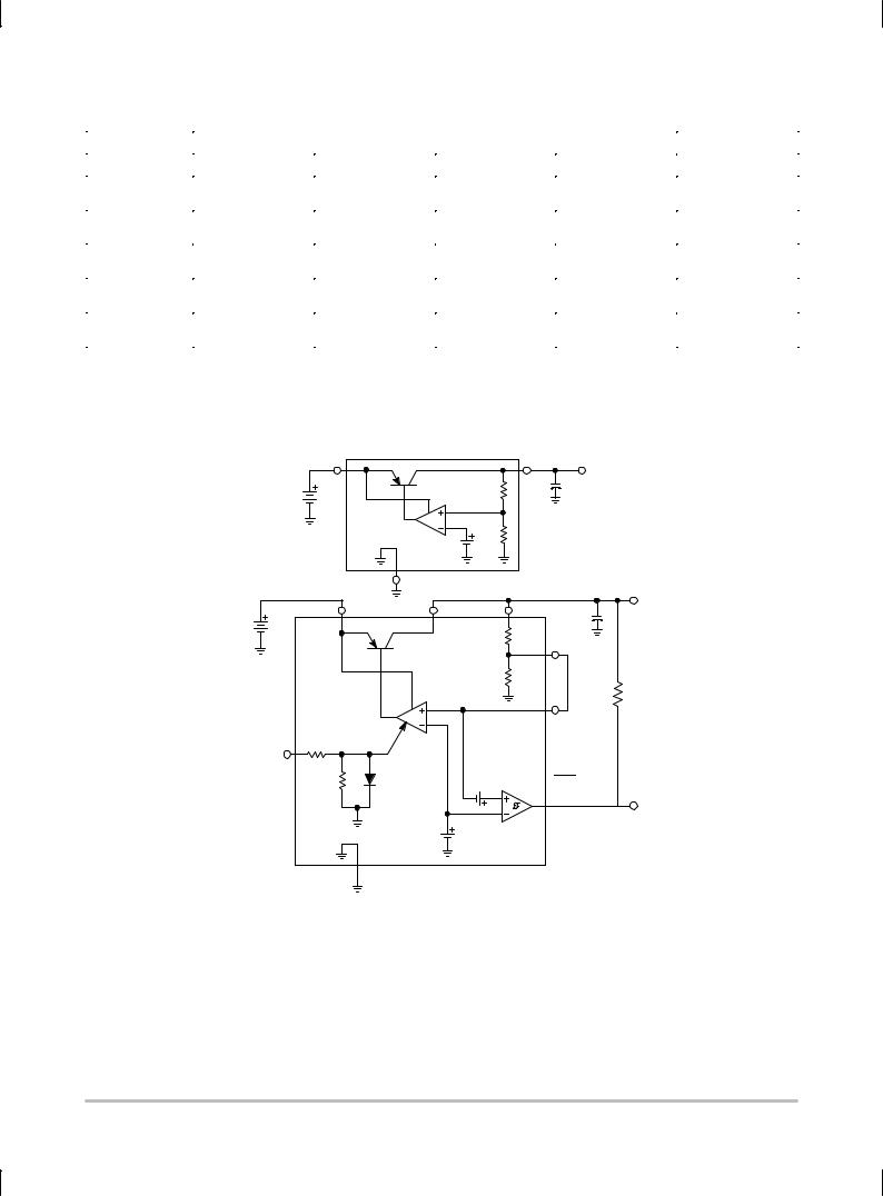
Representative Block Diagrams
Input |
|
Output |
|
5.0 V/100 mA |
|
3 |
|
1 |
|
||
|
1.0 |
μF |
|||
Battery or |
|
182 k |
|||
|
|
|
|||
Unregulated DC |
|
|
|
||
|
|
|
|
||
Error Amplifier |
60 k |
|
|
||
|
1.23 V |
|
|
||
|
|
|
|
||
|
Reference |
LP2950CZ±5.0 |
|||
Gnd |
2 |
||||
|
|
|
|||
Battery or |
Input |
8 |
Output |
1 |
Unregulated DC
|
Error |
Shutdown |
Amplifier |
|
From |
3 60 k |
CMOS/TTL |
50 k |
|
1.23 V
Reference
Gnd  4
4
Sense 2 |
|
5.0 V/100 mA |
|
1.0 |
μF |
||
|
|||
182 k |
VO Tap |
||
|
|||
60 k |
6 |
|
|
|
|
||
|
7 |
330 k |
|
|
|
||
|
Feedback |
||
75 mV/
60 mV Error Output


 To CMOS/TTL 5
Error Detection
Comparator
LP2951CD or CN
This device contains 34 active transistors.
http://onsemi.com
2

LP2950
MAXIMUM RATINGS (TA = 25°C, unless otherwise noted.)
Rating |
|
|
Symbol |
|
|
Value |
|
|
Unit |
||
|
|
|
|
|
|
|
|
|
|
|
|
Input Voltage |
|
|
|
VCC |
|
|
30 |
|
|
|
Vdc |
Power Dissipation and Thermal Characteristics |
|
|
|
|
|
|
|
|
|
|
|
|
|
|
|
|
|
|
|
|
|
|
|
Maximum Power Dissipation |
|
|
|
PD |
|
|
Internally Limited |
|
W |
||
Case 751(SO±8) D Suffix |
|
|
|
|
|
|
|
|
|
|
|
Thermal Resistance, Junction±to±Ambient |
|
|
RθJA |
|
|
180 |
|
|
|
°C/W |
|
Thermal Resistance, Junction±to±Case |
|
|
RθJC |
|
|
45 |
|
|
|
°C/W |
|
Case 369A (DPAK) DT Suffix [Note 1] |
|
|
|
|
|
|
|
|
|
|
|
Thermal Resistance, Junction±to±Ambient |
|
|
RθJA |
|
|
92 |
|
|
|
°C/W |
|
Thermal Resistance, Junction±to±Case |
|
|
RθJC |
|
|
6.0 |
|
|
|
°C/W |
|
Case 29 (TO±226AA/TO±92) Z Suffix |
|
|
|
|
|
|
|
|
|
|
|
Thermal Resistance, Junction±to±Ambient |
|
|
RθJA |
|
|
160 |
|
|
|
°C/W |
|
Thermal Resistance, Junction±to±Case |
|
|
RθJC |
|
|
83 |
|
|
|
°C/W |
|
Case 626 N Suffix |
|
|
|
|
|
|
|
|
|
|
|
Thermal Resistance, Junction±to±Ambient |
|
|
RθJA |
|
|
105 |
|
|
|
°C/W |
|
Case 846A (Micro±8) DM Suffix |
|
|
|
|
|
|
|
|
|
|
|
Thermal Resistance, Junction±to±Ambient |
|
|
RθJA |
|
|
240 |
|
|
|
°C/W |
|
Feedback Input Voltage |
|
|
|
Vfb |
|
|
±1.5 to +30 |
|
|
Vdc |
|
Shutdown Input Voltage |
|
|
|
Vsd |
|
|
±0.3 to +30 |
|
|
Vdc |
|
Error Comparator Output Voltage |
|
|
|
Verr |
|
|
±0.3 to +30 |
|
|
Vdc |
|
Operating Junction Temperature |
|
|
|
TJ |
|
|
±40 to +125 |
|
|
°C |
|
Storage Temperature Range |
|
|
|
Tstg |
|
|
±65 to +150 |
|
|
°C |
|
NOTE: 1. The Junction±to±Ambient Thermal Resistance is determined by PC board copper area per Figure 26. |
|
|
|
|
|
||||||
2. ESD data available upon request. |
|
|
|
|
|
|
|
|
|
|
|
ELECTRICAL CHARACTERISTICS (Vin = VO + 1.0 V, IO = 100 μA, CO = 1.0 μF, TJ = 25°C [Note 1], unless |
|
|
|
||||||||
otherwise noted.) |
|
|
|
|
|
|
|
|
|
|
|
|
|
|
|
|
|
|
|
|
|
||
Characteristic |
Symbol |
|
Min |
|
Typ |
|
Max |
|
Unit |
||
|
|
|
|
|
|
|
|
|
|
|
|
Output Voltage, 5.0 V Versions |
VO |
|
|
|
|
|
|
|
|
V |
|
Vin = 6.0 V, IO = 100 μA, TJ = 25°C |
|
|
|
|
|
|
|
|
|
|
|
LP2950C±5.0/LP2951C |
|
|
|
4.950 |
|
|
5.000 |
|
5.050 |
|
|
LP2950AC±5.0/LP2951AC |
|
|
|
4.975 |
|
|
5.000 |
|
5.025 |
|
|
TJ = ± 40 to +125°C |
|
|
|
|
|
|
|
|
|
|
|
LP2950C±5.0/LP2951C |
|
|
|
4.900 |
|
|
± |
|
5.100 |
|
|
LP2950AC±5.0/LP2951AC |
|
|
|
4.940 |
|
|
± |
|
5.060 |
|
|
Vin = 6.0 to 30 V, IO = 100 μA to 100 mA, TJ = ± 40 to +125°C |
|
|
|
|
|
|
|
|
|
|
|
LP2950C±5.0/LP2951C |
|
|
|
4.880 |
|
|
± |
|
5.120 |
|
|
LP2950AC±5.0/LP2951AC |
|
|
|
4.925 |
|
|
± |
|
5.075 |
|
|
|
|
|
|
|
|
|
|
|
|
|
|
Output Voltage, 3.3 V Versions |
VO |
|
|
|
|
|
|
|
|
V |
|
Vin = 4.3 V, IO = 100 μA, TJ = 25°C |
|
|
|
|
|
|
|
|
|
|
|
LP2950C±3.3/LP2951C±3.3 |
|
|
|
3.267 |
|
|
3.300 |
|
3.333 |
|
|
LP2950AC±3.3/LP2951AC±3.3 |
|
|
|
3.284 |
|
|
3.300 |
|
3.317 |
|
|
TJ = ± 40 to +125°C |
|
|
|
|
|
|
|
|
|
|
|
LP2950C±3.3/LP2951C±3.3 |
|
|
|
3.234 |
|
|
± |
|
3.366 |
|
|
LP2950AC±3.3/LP2951AC±3.3 |
|
|
|
3.260 |
|
|
± |
|
3.340 |
|
|
Vin = 4.3 to 30 V, IO = 100 μA to 100 mA, TJ = ± 40 to +125°C |
|
|
|
|
|
|
|
|
|
|
|
LP2950C±3.3/LP2951C±3.3 |
|
|
|
3.221 |
|
|
± |
|
3.379 |
|
|
LP2950AC±3.3/LP2951AC±3.3 |
|
|
|
3.254 |
|
|
± |
|
3.346 |
|
|
|
|
|
|
|
|
|
|
|
|
|
|
Output Voltage, 3.0 V Versions |
VO |
|
|
|
|
|
|
|
|
V |
|
Vin = 4.0 V, IO = 100 μA, TJ = 25°C |
|
|
|
|
|
|
|
|
|
|
|
LP2950C±3.0/LP2951C±3.0 |
|
|
|
2.970 |
|
|
3.000 |
|
3.030 |
|
|
LP2950AC±3.0/LP2951AC±3.0 |
|
|
|
2.985 |
|
|
3.000 |
|
3.015 |
|
|
TJ = ± 40 to +125°C |
|
|
|
|
|
|
|
|
|
|
|
LP2950C±3.0/LP2951C±3.0 |
|
|
|
2.940 |
|
|
± |
|
3.060 |
|
|
LP2950AC±3.0/LP2951AC±3.0 |
|
|
|
2.964 |
|
|
± |
|
3.036 |
|
|
Vin = 4.0 to 30 V, IO = 100 μA to 100 mA, TJ = ± 40 to +125°C |
|
|
|
|
|
|
|
|
|
|
|
LP2950C±3.0/LP2951C±3.0 |
|
|
|
2.928 |
|
|
± |
|
3.072 |
|
|
LP2950AC±3.0/LP2951AC±3.0 |
|
|
|
2.958 |
|
|
± |
|
3.042 |
|
|
http://onsemi.com
3

LP2950
ELECTRICAL CHARACTERISTICS (continued) (Vin = VO + 1.0 V, IO = 100 μA, CO = 1.0 μF, TJ = 25°C [Note 1], unless otherwise noted.)
Characteristic |
Symbol |
Min |
Typ |
Max |
Unit |
|
|
|
|
|
|
Line Regulation (Vin = VO(nom) +1.0 V to 30 V) [Note 2] |
Regline |
|
|
|
% |
LP2950C±XX/LP2951C/LP2951C±XX |
|
± |
0.08 |
0.20 |
|
LP2950AC±XX/LP2951AC/LP2951AC±XX |
|
± |
0.04 |
0.10 |
|
|
|
|
|
|
|
Load Regulation (IO = 100 μA to 100 mA) |
Regload |
|
|
|
% |
LP2950C±XX/LP2951C/LP2951C±XX |
|
± |
0.13 |
0.20 |
|
LP2950AC±XX/LP2951AC/LP2951AC±XX |
|
± |
0.05 |
0.10 |
|
|
|
|
|
|
|
Dropout Voltage |
VI ± VO |
|
|
|
mV |
IO = 100 μA |
|
± |
30 |
80 |
|
IO = 100 mA |
|
± |
350 |
450 |
|
Supply Bias Current |
ICC |
|
|
|
|
IO = 100 μA |
|
± |
93 |
120 |
μA |
IO = 100 mA |
|
± |
4.0 |
12 |
mA |
Dropout Supply Bias Current (Vin = VO(nom) ± 0.5 V, |
ICCdropout |
± |
110 |
170 |
μA |
IO = 100 μA) [Note 2] |
|
|
|
|
|
Current Limit (VO Shorted to Ground) |
ILimit |
± |
220 |
300 |
mA |
Thermal Regulation |
Regthermal |
± |
0.05 |
0.20 |
%/W |
Output Noise Voltage (10 Hz to 100 kHz) [Note 3] |
Vn |
|
|
|
μVrms |
CL = 1.0 μF |
|
± |
126 |
± |
|
CL = 100 μF |
|
± |
56 |
± |
|
LP2951A/LP2951AC ONLY |
|
|
|
|
|
|
|
|
|
|
|
Reference Voltage (TJ = 25°C) |
Vref |
|
|
|
V |
LP2951C/LP2951C±XX |
|
1.210 |
1.235 |
1.260 |
|
LP2951AC/LP2951AC±XX |
|
1.220 |
1.235 |
1.250 |
|
|
|
|
|
|
|
Reference Voltage (TJ = ± 40 to +125°C) |
Vref |
|
|
|
V |
LP2951C/LP2951C±XX |
|
1.200 |
± |
1.270 |
|
LP2951AC/LP2951AC±XX |
|
1.200 |
± |
1.260 |
|
|
|
|
|
|
|
Reference Voltage (TJ = ± 40 to +125°C) |
Vref |
|
|
|
V |
IO = 100 μA to 100 mA, Vin = 23 to 30 V |
|
|
|
|
|
LP2951C/LP2951C±XX |
|
1.185 |
± |
1.285 |
|
LP2951AC/LP2951AC±XX |
|
1.190 |
± |
1.270 |
|
|
|
|
|
|
|
Feedback Pin Bias Current |
IFB |
± |
15 |
40 |
nA |
ERROR COMPARATOR |
|
|
|
|
|
|
|
|
|
|
|
Output Leakage Current (VOH = 30 V) |
Ilkg |
± |
0.01 |
1.0 |
μA |
Output Low Voltage (Vin = 4.5 V, IOL = 400 μA) |
VOL |
± |
150 |
250 |
mV |
Upper Threshold Voltage (Vin = 6.0 V) |
Vthu |
40 |
45 |
± |
mV |
Lower Threshold Voltage (Vin = 6.0 V) |
Vthl |
± |
60 |
95 |
mV |
Hysteresis (Vin = 6.0 V) |
Vhy |
± |
15 |
± |
mV |
SHUTDOWN INPUT |
|
|
|
|
|
|
|
|
|
|
|
Input Logic Voltage |
Vshtdn |
|
|
|
V |
Logic ª0º (Regulator ªOnº) |
|
0 |
± |
0.7 |
|
Logic ª1º (Regulator ªOffº) |
|
2.0 |
± |
30 |
|
|
|
|
|
|
|
Shutdown Pin Input Current |
Ishtdn |
|
|
|
μA |
Vshtdn = 2.4 V |
|
± |
35 |
50 |
|
Vshtdn = 30 V |
|
± |
450 |
600 |
|
Regulator Output Current in Shutdown Mode |
Ioff |
± |
3.0 |
10 |
μA |
(Vin = 30 V, Vshtdn = 2.0 V, VO = 0, Pin 6 Connected to Pin 7) |
|
|
|
|
|
NOTES: 1. Low duty pulse techniques are used during test to maintain junction temperature as close to ambient as possible.
2. VO(nom) is the part number voltage option.
3. Noise tests on the LP2951 are made with a 0.01 μF capacitor connected across Pins 7 and 1.
http://onsemi.com
4

LP2950
DEFINITIONS
Dropout Voltage ± The input/output voltage differential at which the regulator output no longer maintains regulation against further reductions in input voltage. Measured when the output drops 100 mV below its nominal value (which is measured at 1.0 V differential), dropout voltage is affected by junction temperature, load current and minimum input supply requirements.
Line Regulation ± The change in output voltage for a change in input voltage. The measurement is made under conditions of low dissipation or by using pulse techniques such that average chip temperature is not significantly affected.
Load Regulation ± The change in output voltage for a change in load current at constant chip temperature.
Maximum Power Dissipation ± The maximum total device dissipation for which the regulator will operate within specifications.
Bias Current ± Current which is used to operate the regulator chip and is not delivered to the load.
Output Noise Voltage ± The rms ac voltage at the output, with constant load and no input ripple, measured over a specified frequency range.
Leakage Current ± Current drawn through a bipolar transistor collector±base junction, under a specified collector voltage, when the transistor is ªoffº.
Upper Threshold Voltage ± Voltage applied to the comparator input terminal, below the reference voltage which is applied to the other comparator input terminal, which causes the comparator output to change state from a logic ª0º to ª1º.
Lower Threshold Voltage ± Voltage applied to the comparator input terminal, below the reference voltage which is applied to the other comparator input terminal, which causes the comparator output to change state from a logic ª1º to ª0º.
Hysteresis ± The difference between Lower Threshold voltage and Upper Threshold voltage.
Figure 1. Quiescent Current
(mA) |
10 |
|
|
|
|
|
|
|
|
|
|
|
|
|
|
|
|
|
|
|
|
|
|
|
|
|
|
|
|
|
|
|
|
|
|
|
|
|
|
|
|
|
|
|
|
|
|
|
|
|
|
|
|
|
|
|
|
|
|
|
|
CURRENTBIAS |
1.0 |
|
|
|
|
|
|
|
|
|
|
|
|
|
|
|
|
|
|
|
|
|
|
|
|
|
|
|
|
|
|
|
|
|
|
|
|
|
|
|
|
|
|
|
|
|
|
|
|
|
|
|
|
|
|
|
|
|
|
||
LP2950/LP2951 |
|
|
|
|
|
|
|
|
|
|
|
|
|
|
|
|
|
|
|
|
|
|
|
|
|
|
|
|
|
|
|
|
|
|
|
|
|
|
|
|
|
|
|
|
|
|
|
|
|
|
|
|
|
|
|
|
|
|
|
||
0.1 |
|
|
|
|
|
|
|
|
|
|
|
|
|
|
|
|
|
|
|
|
|
|
|
|
|
|
|
|
|
|
|
|
|
|
|
|
|
|
|
|
|
|
|
|
|
|
|
|
|
|
|
|
|
|
|
|
|
|
|
||
|
|
|
|
|
|
|
|
|
|
|
|
|
|
|
|
|
|
|
|
|
|
|
|
|
|
|
|
|
||
|
|
|
|
|
|
|
|
|
|
|
|
|
|
|
|
|
|
|
|
|
|
|
|
|
|
|
|
|
||
|
|
|
|
|
|
|
|
|
|
|
|
|
|
|
|
|
|
|
|
|
|
|
|
|
|
|
|
|
||
|
|
|
|
|
|
|
|
|
|
|
|
|
|
|
|
|
|
|
|
|
|
|
|
|
|
|
|
|
||
|
|
|
|
|
|
|
|
|
|
|
|
|
|
|
|
|
|
|
|
|
|
|
|
|
|
|
|
|
||
|
|
|
|
|
|
|
|
|
|
|
|
|
|
|
|
|
|
|
|
|
|
|
|
|
|
|
|
|
|
|
|
|
|
|
|
|
|
|
|
|
|
|
|
|
|
|
|
|
|
|
|
|
|
|
|
|
|
|
|
|
|
|
0.01 |
|
|
|
|
|
|
|
|
|
|
|
|
|
|
|
|
|
|
|
|
|
|
|
|
|
|
|
|
|
|
|
|
|
|
|
|
|
|
|
|
|
|
|
|
|
|
|
|
|
|
|
|
|
|
|
|
|
|
|
|
|
|
|
|
|
|
|
|
|
|
|
|
|
|
|
|
|
|
|
|
|
|
|
|
|
|
|
|
|
|
|
|
|
|
|
|
|
|
|
|
|
|
|
|
|
|
|
|
|
|
|
|
|
|
|
|
|
|
|
|
|
|
|
|
|
|
|
|
|
|
|
|
|
|
|
|
|
|
|
|
|
|
|
|
|
|
|
|
|
|
|
|
|
|
|
|
|
|
|
|
|
|
|
|
|
|
|
|
|
|
|
|
|
|
|
|
|
|
|
|
|
|
|
|
|
|
|
|
|
|
|
|
|
|
|
|
|
|
|
|
|
|
|
|
|
|
|
|
|
|
|
|
|
|
|
|
|
1.0 |
|
10 |
100 |
|||||||||||||||||||||||||
|
0.1 |
|
||||||||||||||||||||||||||||
IL, LOAD CURRENT (mA)
Figure 3. Input Current
|
250 |
|
|
|
|
|
|
200 |
|
|
0.1 mA Load Current |
|
|
(μA) |
|
|
|
|
||
|
|
|
|
|
|
|
CURRENT |
150 |
|
|
|
|
|
100 |
|
|
|
|
|
|
BIAS |
|
|
|
|
|
|
|
|
|
No Load |
|
|
|
|
50 |
|
|
|
|
|
|
0 |
5.0 |
10 |
15 |
20 |
25 |
|
0 |
|||||
|
|
|
Vin, INPUT VOLTAGE (V) |
|
|
|
Figure 2. Dropout Characteristics
|
6.0 |
|
|
|
|
|
|
|
|
LP2951C |
|
|
|
|
|
(V) |
5.0 |
TA = 25°C |
|
|
|
|
|
|
|
|
RL = 50 k |
|
|
|
|
VOLTAGE |
4.0 |
|
|
|
|
|
|
|
|
|
|
|
|
||
3.0 |
|
|
|
|
|
|
|
, OUTPUT |
|
|
|
|
|
|
|
2.0 |
|
|
RL = 50 Ω |
|
|
|
|
|
|
|
|
|
|
||
|
|
|
|
|
|
|
|
out |
1.0 |
|
|
|
|
|
|
V |
|
|
|
|
|
|
|
|
0 |
1.0 |
2.0 |
3.0 |
4.0 |
5.0 |
6.0 |
|
0 |
||||||
|
|
|
Vin, INPUT VOLTAGE (V) |
|
|
||
Figure 4. Output Voltage versus Temperature
|
5.00 |
|
|
|
|
|
(V) |
4.99 |
|
|
|
|
|
|
|
|
|
|
|
|
VOLTAGE |
4.98 |
|
|
|
|
|
OUTPUT, |
4.97 |
|
|
|
|
|
|
|
|
|
|
|
|
out |
4.96 |
|
|
|
|
|
V |
|
|
|
|
LP2951C |
|
|
|
|
|
|
|
|
|
4.95 |
0 |
50 |
100 |
150 |
200 |
|
± 50 |
|||||
|
|
|
TA, AMBIENT TEMPERATURE (°C) |
|
|
|
http://onsemi.com
5
 Loading...