


LM317LZRP
Motorola LM317LZRP, LM317LZRA, LM317LBZRA, LM317LBZ, LM317LBDR2 Datasheet
...
SEMICONDUCTOR
TECHNICAL DATA
LOW CURRENT
THREE–TERMINAL
ADJUSTABLE POSITIVE
VOLTAGE REGULATOR
ORDERING INFORMATION
Order this document by LM317L/D
Z SUFFIX
PLASTIC PACKAGE
CASE 29
Pin 1. Adjust
2. V
out
3. V
in
3
1
2
D SUFFIX
PLASTIC PACKAGE
CASE 751
(SOP–8*)
1
8
Pin 1. V
in
2. V
out
3. V
out
4. Adjust
5. N.C.
6. V
out
7. V
out
8. N.C.
* SOP–8 is an internally modified SO–8 pack-
age. Pins 2, 3, 6 and 7 are electrically common
to the die attach flag. This internal lead frame
modification decreases package thermal resis-
tance and increases power dissipation capabili-
ty when appropriately mounted on a printed cir-
cuit board. SOP–8 conforms to all external di-
mensions of the standard SO–8 package.
Operating
Temperature Range
Device Package
LM317LD
LM317LZ
LM317LBZ
SOP–8
Plastic
Plastic
T
J
= –40° to +125°C
T
J
= 0° to +125°C
LM317LBD SOP–8
1
MOTOROLA ANALOG IC DEVICE DATA
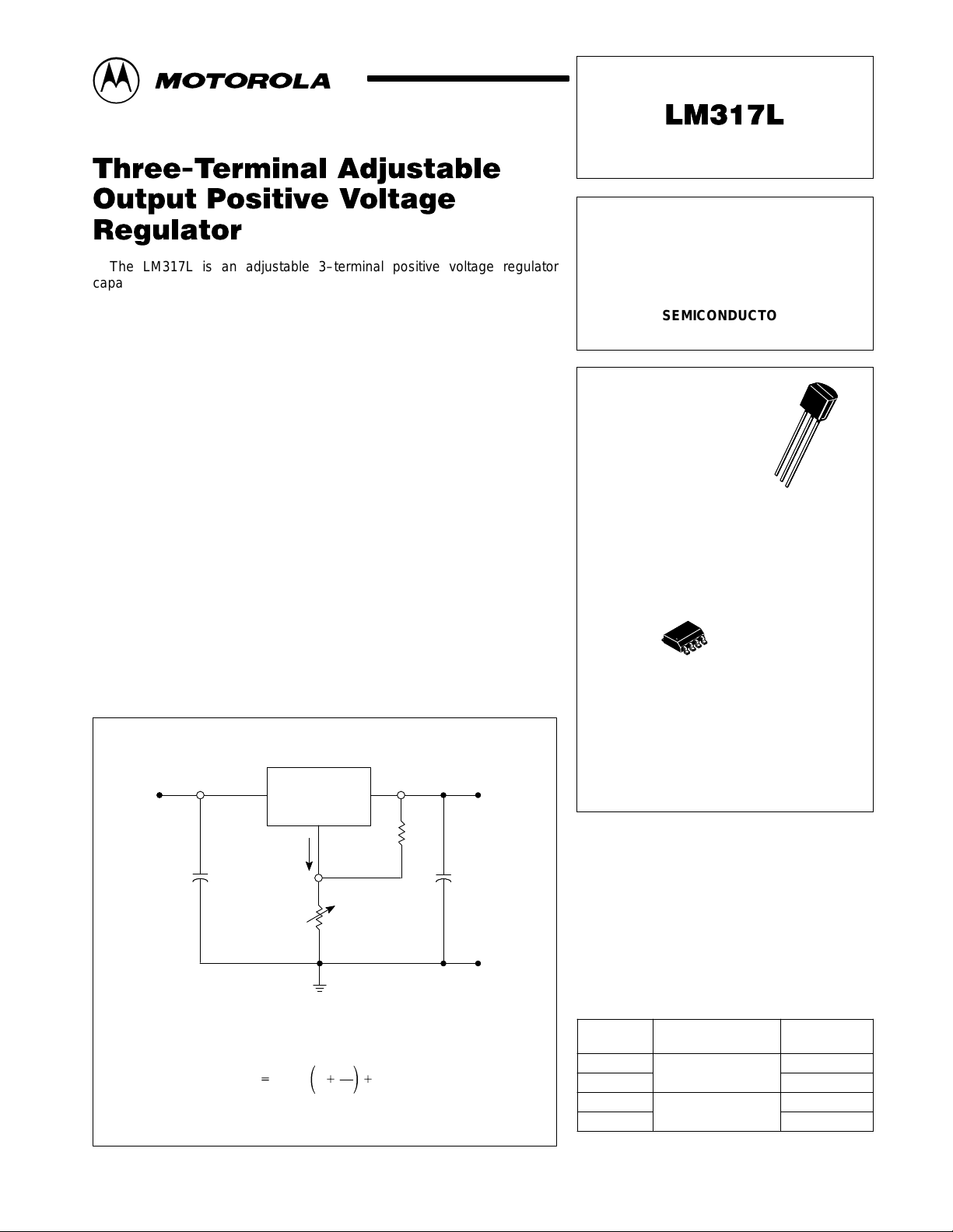
The LM317L is an adjustable 3–terminal positive voltage regulator
capable of supplying in excess of 100 mA over an output voltage range of
1.2 V to 37 V. This voltage regulator is exceptionally easy to use and
requires only two external resistors to set the output voltage. Further, it
employs internal current limiting, thermal shutdown and safe area
compensation, making them essentially blow–out proof.
The LM317L serves a wide variety of applications including local, on card
regulation. This device can also be used to make a programmable output
regulator, or by connecting a fixed resistor between the adjustment and
output, the LM317L can be used as a precision current regulator.
• Output Current in Excess of 100 mA
• Output Adjustable Between 1.2 V and 37 V
• Internal Thermal Overload Protection
• Internal Short Circuit Current Limiting
• Output Transistor Safe–Area Compensation
• Floating Operation for High Voltage Applications
• Standard 3–Lead Transistor Package
• Eliminates Stocking Many Fixed Voltages
Simplified Application
* C
in
is required if regulator is located an appreciable
** distance from power supply filter.
** C
O
is not needed for stability, however,
** it does improve transient response.
Since I
Adj
is controlled to less than 100
µ
A, the error
associated with this term is negligible in most applications.
LM317L
V
in
V
out
R
1
240
R
2
Adjust
I
Adj
C
in
*
0.1
µ
F
+
C
O
**
1.0
µ
F
V
out
+
1.25 V
ǒ
1
)
R
2
R
1
Ǔ
)
I
Adj
R
2
Motorola, Inc. 1996 Rev 1
LM317L
2
MOTOROLA ANALOG IC DEVICE DATA
MAXIMUM RATINGS
Rating Symbol Value Unit
Input–Output V oltage Differential V
I
–V
O
40 Vdc
Power Dissipation P
D
Internally Limited W
Operating Junction Temperature Range T
J
–40 to +125 °C
Storage Temperature Range T
stg
–65 to +150 °C
ELECTRICAL CHARACTERISTICS (V
I
–V
O
= 5.0 V; I
O
= 40 mA; T
J
= T
low
to T
high
[Note 1]; I
max
and P
max
[Note 2];
unless otherwise noted.)
LM317L, LB
Characteristics Figure Symbol Min Typ Max Unit
Line Regulation (Note 3)
T
A
= 25°C, 3.0 V ≤ V
I
– V
O
≤ 40 V
1 Reg
line
– 0.01 0.04 %/V
Load Regulation (Note 3), T
A
= 25°C
10 mA ≤ I
O
≤ I
max
– LM317L
V
O
≤ 5.0 V
V
O
≥ 5.0 V
2 Reg
load
–
–
5.0
0.1
25
0.5
mV
% V
O
Adjustment Pin Current 3 I
Adj
– 50 100 µA
Adjustment Pin Current Change
2.5 V ≤ V
I
– V
O
≤ 40 V, P
D
≤ P
max
10 mA ≤ I
O
≤ I
max
– LM317L
1, 2 ∆I
Adj
– 0.2 5.0 µA
Reference Voltage
3.0 V ≤ V
I
– V
O
≤ 40 V, P
D
≤ P
max
10 mA ≤ I
O
≤ I
max
– LM317L
3 V
ref
1.20 1.25 1.30 V
Line Regulation (Note 3)
3.0 V ≤ V
I
– V
O
≤ 40 V
1 Reg
line
– 0.02 0.07 %/V
Load Regulation (Note 3)
10 mA ≤ I
O
≤ I
max
– LM317L
V
O
≤ 5.0 V
V
O
≥ 5.0 V
2 Reg
load
–
–
20
0.3
70
1.5
mV
% V
O
Temperature Stability (T
low
≤ T
J
≤ T
high
) 3 T
S
– 0.7 – % V
O
Minimum Load Current to Maintain Regulation (V
I
– V
O
= 40 V) 3 I
Lmin
– 3.5 10 mA
Maximum Output Current
V
I
– V
O
≤ 6.25 V, P
D
≤ P
max
, Z Package
V
I
– V
O
≤ 40 V, P
D
≤ P
max
, T
A
= 25°C, Z Package
3 I
max
100
–
200
20
–
–
mA
RMS Noise, % of V
O
T
A
= 25°C, 10 Hz ≤ f ≤ 10 kHz
N – 0.003 – % V
O
Ripple Rejection (Note 4)
V
O
= 1.2 V, f = 120 Hz
C
Adj
= 10 µF, V
O
= 10.0 V
4 RR
60
–
80
80
–
–
dB
Long Term Stability, T
J
= T
high
(Note 5)
T
A
= 25°C for Endpoint Measurements
3 S – 0.3 1.0 %/1.0 k
Hrs.
Thermal Resistance, Junction–to–Case
Z Package
R
θJC
– 83 – °C/W
Thermal Resistance, Junction–to–Air
Z Package
R
θJA
– 160 – °C/W
NOTES: 1. T
low
to T
high
= 0° to +125°C for LM317L –40° to +125°C for LM317LB
2.I
max
= 100 mA P
max
= 625 mW
3.Load and line regulation are specified at constant junction temperature. Changes in V
O
due to heating effects must be taken into account separately.
Pulse testing with low duty cycle is used.
4.C
Adj
, when used, is connected between the adjustment pin and ground.
5.Since Long–T erm Stability cannot be measured on each device before shipment, this specification is an engineering estimate of average stability
from lot to lot.
LM317L
3
MOTOROLA ANALOG IC DEVICE DATA
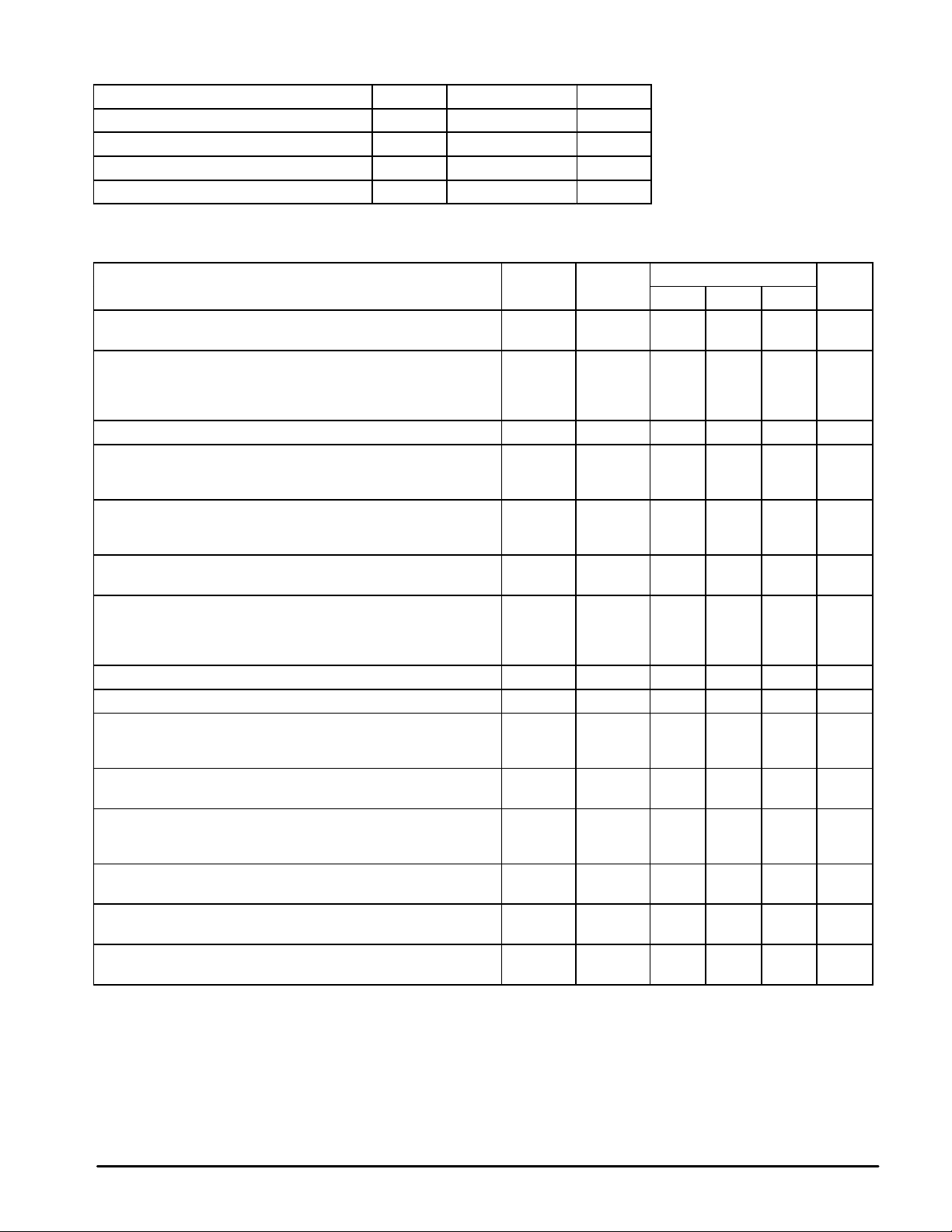
Representative Schematic Diagram
18k
6.8V
6.8V
350
300 300 300 3.0k 30
0
70
200
k
2.560
5
0
130
8.67k
500
40
0
2.4k
12.8k
V
out
5.1k
6.3V
2.0k 6.0k
Adjust
V
in
180 180
10
pF
10
pF
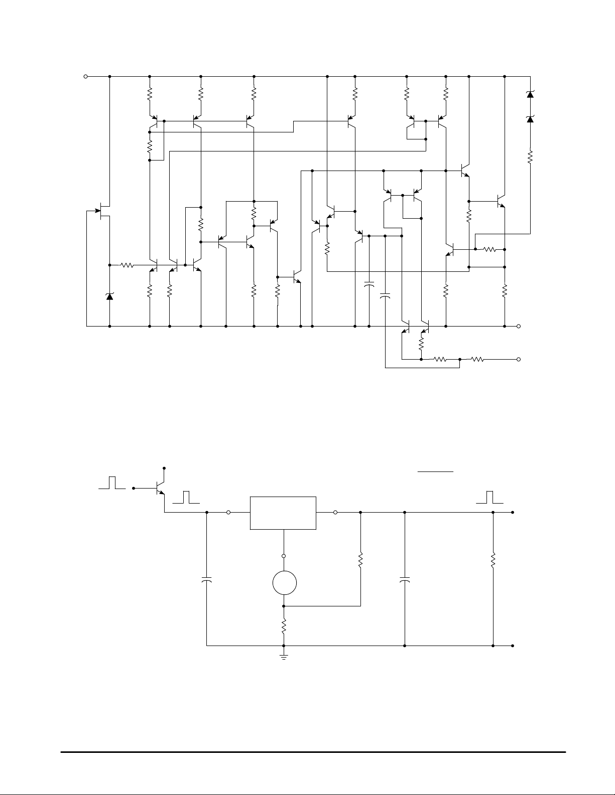
* Pulse Testing Required:
1% Duty Cycle is suggested.
Line Regulation (%/V) =
V
OH
– V
OL
x 100
*
V
CC
V
IH
V
IL
V
in
V
out
V
OH
V
OL
R
L
+
1
µ
FC
O
240
1%
R
1
Adjust
R2
1
%
C
in
0.1
µ
F
LM317L
I
Adj
Figure 1. Line Regulation and ∆I
Adj
/Line T est Circuit
V
OL
LM317L
4
MOTOROLA ANALOG IC DEVICE DATA
* Pulse Testing Required:
1% Duty Cycle is suggested.
Load Regulation (mV) = V
O
(min Load) –V
O
(max Load)
Load Regulation (% V
O
) =
V
O
(min Load) – V
O
(max Load)
X
100
V
O
(min Load)
V
O
(max Load)
LM317L
C
in
0.1
µ
F
Adjust
R
2
1%
C
O
1.0
µ
F
+
*
R
L
(max Load)
R
L
(min Load)
V
out
R
1
240
1%
V
in
*V
in
I
Adj
I
L
Figure 2. Load Regulation and ∆I
Adj
/Load Test Circuit
V
O
(min Load)
Pulse Testing Required:
1% Duty Cycle is suggested.
LM317L
V
in
V
out
Adjust
R
1
240
1%
+
1
µ
FC
O
R
L
C
in
R
2
1%
To Calculate R
2
:
V
out
= I
SET
R
2
+ 1.250 V
Assume I
SET
= 5.25 mA
I
L
I
Adj
I
SET
V
ref
V
O
V
I
0.1
µ
F
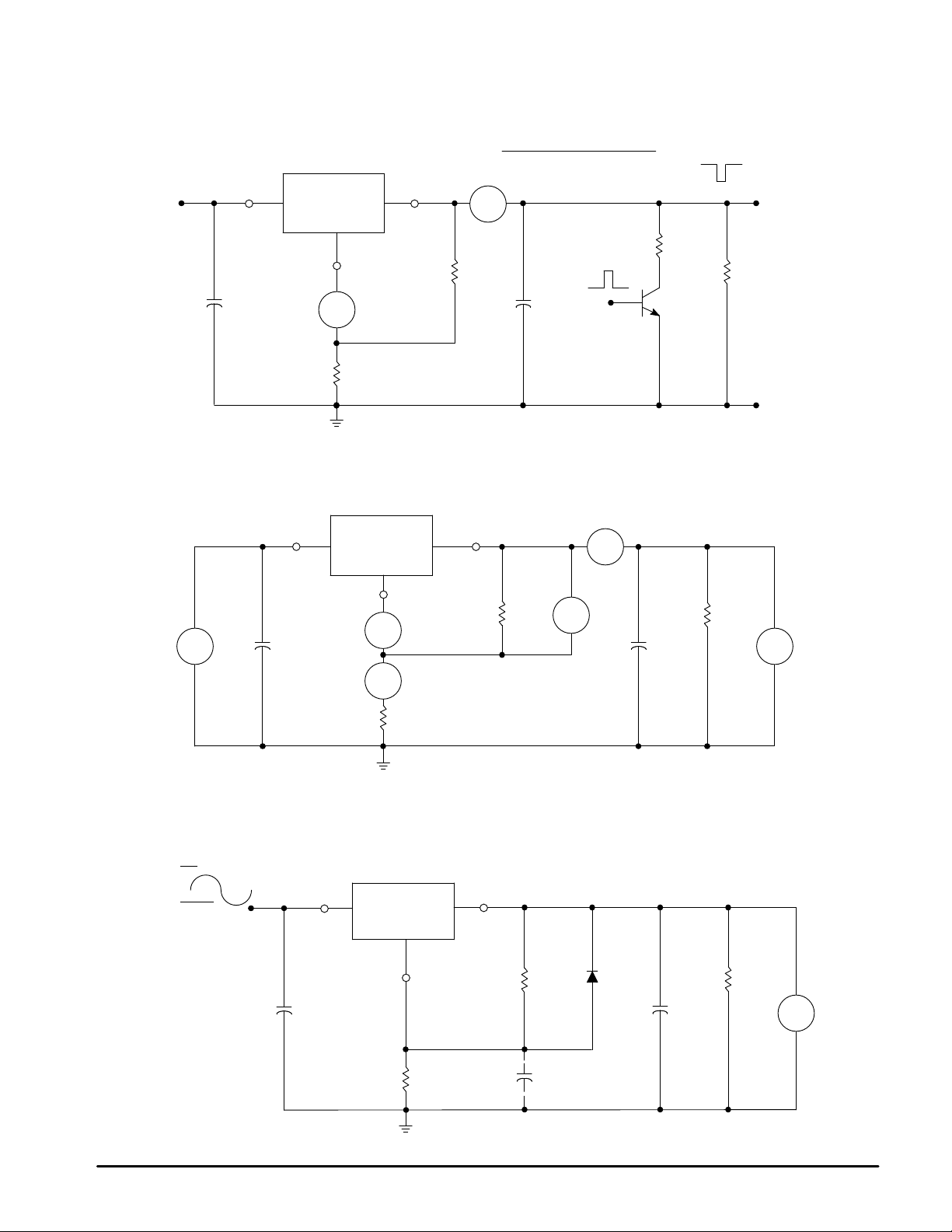
Figure 3. Standard T est Circuit
LM317L
V
in
V
out
V
out
= 1.25 V
R
L
C
in
0.1
µ
F
Adjust
R
1
240
1%
D
1
*
1N4002
C
O
+
1
µ
F
14.30V
4.30V
R
2
1.65K
1%
**
10
µ
F
+
*D
1
Discharges C
Adj
if Output is Shorted to Ground.
f = 120 Hz
V
O
**C
Adj
provides an AC ground to the adjust pin.
Figure 4. Ripple Rejection T est Circuit
 Loading...