


MOTOROLA LM2576T-015, LM2576T-012, LM2576T-3.3, LM2576TV-ADJ, LM2576TV-3.3 Datasheet
...Order this document by LM2576/D
|
|
|
|
|
|
LM2576 |
||
Easy |
Switcher |
3.0 |
A |
|
|
|
||
Step-Down |
Voltage |
Regulator |
EASY SWITCHER |
|||||
The LM2576 series of regulators are monolithic integrated circuits ideally |
||||||||
3.0 A STEP±DOWN |
||||||||
suited for easy and convenient design of a step±down switching regulator |
||||||||
VOLTAGE REGULATOR |
||||||||
(buck converter). All circuits of this series are capable of driving a 3.0 A load |
||||||||
with excellent line and load regulation. These devices are available in fixed |
|
SEMICONDUCTOR |
||||||
output voltages of 3.3 V, 5.0 V, 12 V, 15 V, and an adjustable output version. |
|
|||||||
These regulators were designed to minimize the number of external |
|
TECHNICAL DATA |
||||||
components to simplify the power supply design. Standard series of |
|
|
|
|||||
inductors optimized for use with the LM2576 are offered by several different |
|
|
|
|||||
inductor manufacturers. |
|
|
|
|
|
|
||
Since the LM2576 converter is a switch±mode power supply, its efficiency |
T SUFFIX |
|
||||||
is significantly |
higher in comparison |
with popular |
three±terminal linear |
|
||||
PLASTIC PACKAGE |
|
|||||||
regulators, especially with higher input voltages. In many cases, the power |
|
|||||||
CASE 314D |
|
|||||||
dissipated is so low that no heatsink is required or its size could be reduced |
|
|||||||
|
1 |
|
||||||
dramatically. |
|
|
|
|
|
|
||
|
|
|
|
Pin 1. |
Vin |
|
||
A standard series of inductors optimized for use with the LM2576 are |
|
|||||||
2. |
Output |
5 |
||||||
available from several different manufacturers. This feature greatly simplifies |
3. |
Ground |
||||||
|
||||||||
the design of switch±mode power supplies. |
|
4. |
Feedback |
|
||||
The LM2576 features include a guaranteed ±4% tolerance on output |
5. ON/OFF |
|
||||||
|
|
|
||||||
voltage within specified input voltages and output load conditions, and ±10% |
|
|
|
|||||
on the oscillator frequency (±2% over 0°C to 125°C). External shutdown is |
|
|
|
|||||
included, featuring 80 μA (typical) standby current. The output switch |
|
|
|
|||||
includes cycle±by±cycle current limiting, as well as thermal shutdown for full |
TV SUFFIX |
1 |
||||||
protection under fault conditions. |
|
|
PLASTIC PACKAGE |
|
||||
Features |
|
|
|
|
CASE 314B |
|
||
|
|
|
|
|
|
5 |
||
• 3.3 V, 5.0 V, 12 V, 15 V, and Adjustable Output Versions |
Heatsink surface |
|
||||||
• Adjustable Version Output Voltage Range, 1.23 to 37 V ±4% Maximum |
connected to Pin 3. |
|
||||||
Over Line and Load Conditions |
|
|
|
|
|
|||
• Guaranteed 3.0 A Output Current |
|
|
|
|
|
|||
• Wide Input Voltage Range |
|
|
|
D2T SUFFIX |
|
|||
• Requires Only 4 External Components |
|
|
||||||
|
PLASTIC PACKAGE |
|
||||||
• 52 kHz Fixed Frequency Internal Oscillator |
|
CASE 936A |
1 |
|||||
|
(D2PAK) |
|||||||
• TTL Shutdown Capability, Low Power Standby Mode |
5 |
|||||||
|
|
|||||||
|
|
|
||||||
• High Efficiency |
|
|
|
Heatsink surface (shown as terminal 6 in case outline |
||||
• Uses Readily Available Standard Inductors |
|
|||||||
|
|
drawing) is connected to Pin 3. |
||||||
• Thermal Shutdown and Current Limit Protection |
|
|
|
|
||||
Applications
•Simple High±Efficiency Step±Down (Buck) Regulator
•Efficient Pre±Regulator for Linear Regulators
•On±Card Switching Regulators
•Positive to Negative Converter (Buck±Boost)
•Negative Step±Up Converters
•Power Supply for Battery Chargers
DEVICE TYPE/NOMINAL OUTPUT VOLTAGE
LM2576±3.3 |
3.3 V |
LM2576±5 |
5.0 V |
LM2576±12 |
12 V |
LM2576±15 |
15 V |
LM2576±ADJ |
1.23 V to 37 V |
|
|
ORDERING INFORMATION
|
Operating |
|
Device |
Temperature Range |
Package |
|
|
|
LM2576T±XX |
|
Straight Lead |
|
|
|
LM2576TV±XX |
TJ = ±40° to +125°C |
Vertical Mount |
LM2576D2T±XX |
|
Surface Mount |
|
|
|
XX = Voltage Option, i.e. 3.3, 5, 12, 15 V; and ADJ for
Adjustable Output.
Motorola, Inc. 1999 |
Rev 1, 07/1999 |
LM2576
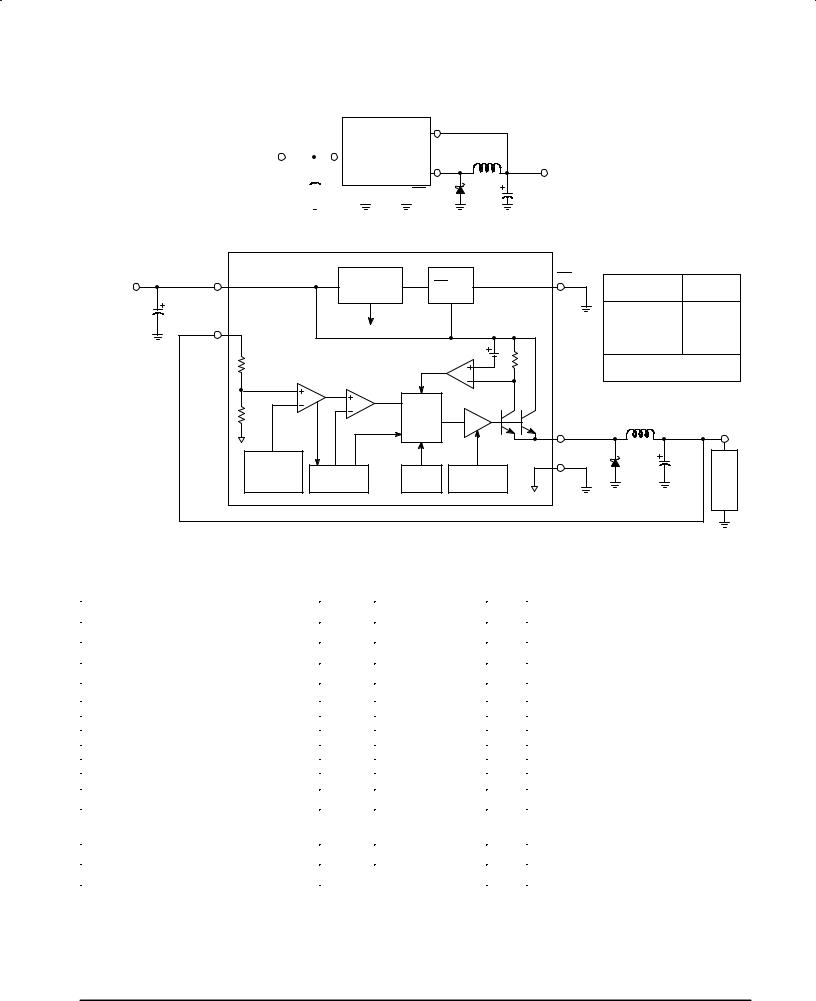
Figure 1. Block Diagram and Typical Application
Typical Application (Fixed Output Voltage Versions)
7.0 V ± 40 V |
|
|
|
|
|
|
+Vin |
||
Unregulated |
|
|
|
|
|
|
|
|
|
DC Input |
|
1 |
|||||||
|
|
Cin |
|
|
|
|
|
|
|
|
|
|
|
|
|
|
|
||
|
100 μF |
|
|
|
|
||||
|
|
|
|
|
|
|
|
|
|
LM2576
3 Gnd 5
Gnd 5
Feedback |
|
|
|
4 |
L1 |
|
|
Output |
100 μH |
|
|
|
|
|
|
2 |
D1 |
Cout |
|
ON/OFF |
1N5822 |
μF |
|
|
|
1000 |
|
5.0 V Regulated
Output 3.0 A Load
|
Representative Block Diagram and Typical Application |
|
|
|
|||||
Unregulated |
+Vin |
|
3.1 V Internal |
ON/OFF |
ON/OFF |
Output |
|
R2 |
|
DC Input |
1 |
|
Regulator |
|
Voltage Versions |
(Ω) |
|||
|
|
|
5 |
||||||
|
|
|
|
|
|
|
1.7 k |
||
|
Cin |
|
|
|
|
|
3.3 V |
|
|
|
4 |
|
|
|
|
|
5.0 V |
|
3.1 k |
|
|
|
|
|
|
12 V |
|
8.84 k |
|
|
|
|
|
|
|
|
|
||
|
Feedback |
|
|
Current |
|
|
15 V |
|
11.3 k |
|
|
|
|
|
|
For adjustable version |
|
||
|
R2 |
Fixed Gain |
|
Limit |
|
|
|
||
|
|
Error Amplifier Comparator |
|
|
|
R1 = open, R2 = 0 Ω |
|
||
|
|
|
|
|
|
|
|
||
|
R1 |
|
|
|
Driver |
|
|
|
Regulated |
|
Freq |
|
Latch |
|
|
|
|
Output |
|
|
1.0 k |
|
|
|
L1 |
|
|||
|
Shift |
|
|
|
Output |
|
Vout |
||
|
|
|
|
|
|
|
|||
|
|
18 kHz |
|
|
1.0 Amp |
2 |
|
|
|
|
1.235 V |
|
|
|
|
|
|||
|
52 kHz |
|
Switch |
Gnd |
D1 |
Cout |
|
||
|
Band±Gap |
Reset |
Thermal |
3 |
|
|
Load |
||
|
Reference |
Oscillator |
Shutdown |
|
|
||||
|
|
|
|
|
|||||
ABSOLUTE MAXIMUM RATINGS (Absolute Maximum Ratings indicate limits beyond which damage to the device may occur.)
|
|
Rating |
Symbol |
Value |
Unit |
|
|
|
|
|
|
|
Maximum Supply Voltage |
Vin |
45 |
V |
|
|
|
|
± |
±0.3 V ≤ V ≤ +Vin |
V |
|
ON/OFF Pin Input Voltage |
||||
|
Output Voltage to Ground (Steady±State) |
± |
±1.0 |
V |
|
|
|
|
|
|
|
|
Power Dissipation |
|
|
|
|
|
Case 314B and 314D (TO±220, 5±Lead) |
PD |
Internally Limited |
W |
|
|
Thermal Resistance, Junction±to±Ambient |
RθJA |
65 |
°C/W |
|
|
Thermal Resistance, Junction±to±Case |
RθJC |
5.0 |
°C/W |
|
|
Case 936A (D2PAK) |
P |
Internally Limited |
W |
|
|
|
|
D |
|
°C/W |
|
Thermal Resistance, Junction±to±Ambient |
RθJA |
70 |
||
|
Thermal Resistance, Junction±to±Case |
RθJC |
5.0 |
°C/W |
|
|
Storage Temperature Range |
Tstg |
±65 to +150 |
°C |
|
|
Minimum ESD Rating (Human Body Model: |
± |
2.0 |
kV |
|
|
C = 100 pF, R = 1.5 kΩ) |
|
|
|
|
|
|
|
|
|
|
|
Lead Temperature (Soldering, 10 seconds) |
± |
260 |
°C |
|
|
|
|
|
|
|
|
Maximum Junction Temperature |
TJ |
150 |
°C |
|
NOTE: ESD data available upon request.
2 |
MOTOROLA ANALOG IC DEVICE DATA |

LM2576
OPERATING RATINGS (Operating Ratings indicate conditions for which the device is intended to be functional, but do not guarantee specific performance limits. For guaranteed specifications and test conditions, see the Electrical Characteristics.)
Rating |
Symbol |
Value |
Unit |
|
|
|
|
Operating Junction Temperature Range |
TJ |
±40 to +125 |
°C |
Supply Voltage |
Vin |
40 |
V |
SYSTEM PARAMETERS ([Note 1] Test Circuit Figure 15)
ELECTRICAL CHARACTERISTICS (Unless otherwise specified, Vin = 12 V for the 3.3 V, 5.0 V, and Adjustable version, Vin = 25 V for
the 12 V version, and Vin = 30 V for the 15 V version. ILoad = 500 mA. For typical values TJ = 25°C, for min/max values TJ is the operating junction temperature range that applies [Note 2], unless otherwise noted.)
Characteristics |
Symbol |
Min |
Typ |
Max |
Unit |
|
|
|
|
|
|
LM2576±3.3 ([Note 1] Test Circuit Figure 15) |
|
|
|
|
|
|
|
|
|
|
|
Output Voltage (Vin = 12 V, ILoad = 0.5 A, TJ = 25°C) |
Vout |
3.234 |
3.3 |
3.366 |
V |
Output Voltage (6.0 V ≤ Vin ≤ 40 V, 0.5 A ≤ ILoad ≤ 3.0 A) |
Vout |
|
|
|
V |
TJ = 25°C |
|
3.168 |
3.3 |
3.432 |
|
TJ = ±40 to +125°C |
|
3.135 |
± |
3.465 |
|
Efficiency (Vin = 12 V, ILoad = 3.0 A) |
η |
± |
75 |
± |
% |
LM2576±5 ([Note 1] Test Circuit Figure 15) |
|
|
|
|
|
|
|
|
|
|
|
Output Voltage (Vin = 12 V, ILoad = 0.5 A, TJ = 25°C) |
Vout |
4.9 |
5.0 |
5.1 |
V |
Output Voltage (8.0 V ≤ Vin ≤ 40 V, 0.5 A ≤ ILoad ≤ 3.0 A) |
Vout |
|
|
|
V |
TJ = 25°C |
|
4.8 |
5.0 |
5.2 |
|
TJ = ±40 to +125°C |
|
4.75 |
± |
5.25 |
|
Efficiency (Vin = 12 V, ILoad = 3.0 A) |
η |
± |
77 |
± |
% |
LM2576±12 ([Note 1] Test Circuit Figure 15) |
|
|
|
|
|
|
|
|
|
|
|
Output Voltage (Vin = 25 V, ILoad = 0.5 A, TJ = 25°C) |
Vout |
11.76 |
12 |
12.24 |
V |
Output Voltage (15 V ≤ Vin ≤ 40 V, 0.5 A ≤ ILoad ≤ 3.0 A) |
Vout |
|
|
|
V |
TJ = 25°C |
|
11.52 |
12 |
12.48 |
|
TJ = ±40 to +125°C |
|
11.4 |
± |
12.6 |
|
Efficiency (Vin = 15 V, ILoad = 3.0 A) |
η |
± |
88 |
± |
% |
LM2576±15 ([Note 1] Test Circuit Figure 15) |
|
|
|
|
|
|
|
|
|
|
|
Output Voltage (Vin = 30 V, ILoad = 0.5 A, TJ = 25°C) |
Vout |
14.7 |
15 |
15.3 |
V |
Output Voltage (18 V ≤ Vin ≤ 40 V, 0.5 A ≤ ILoad ≤ 3.0 A) |
Vout |
|
|
|
V |
TJ = 25°C |
|
14.4 |
15 |
15.6 |
|
TJ = ±40 to +125°C |
|
14.25 |
± |
15.75 |
|
Efficiency (Vin = 18 V, ILoad = 3.0 A) |
η |
± |
88 |
± |
% |
LM2576 ADJUSTABLE VERSION ([Note 1] Test Circuit Figure 15) |
|
|
|
|
|
|
|
|
|
|
|
Feedback Voltage (Vin = 12 V, ILoad = 0.5 A, Vout = 5.0 V, TJ = 25°C) |
Vout |
1.217 |
1.23 |
1.243 |
V |
Feedback Voltage (8.0 V ≤ Vin ≤ 40 V, 0.5 A ≤ ILoad ≤ 3.0 A, Vout = 5.0 V) |
Vout |
|
|
|
V |
TJ = 25°C |
|
1.193 |
1.23 |
1.267 |
|
TJ = ±40 to +125°C |
|
1.18 |
± |
1.28 |
|
Efficiency (Vin = 12 V, ILoad = 3.0 A, Vout = 5.0 V) |
η |
± |
77 |
± |
% |
NOTES: 1. External components such as the catch diode, inductor, input and output capacitors can affect switching regulator system performance. When the LM2576 is used as shown in the Figure 15 test circuit, system performance will be as shown in system parameters section.
2. Tested junction temperature range for the LM2576: |
Tlow = ±40°C |
Thigh = +125°C |
MOTOROLA ANALOG IC DEVICE DATA |
3 |
|

LM2576
DEVICE PARAMETERS
ELECTRICAL CHARACTERISTICS (Unless otherwise specified, Vin = 12 V for the 3.3 V, 5.0 V, and Adjustable version, Vin = 25 V for
the 12 V version, and Vin = 30 V for the 15 V version. ILoad = 500 mA. For typical values TJ = 25°C, for min/max values TJ is the operating junction temperature range that applies [Note 2], unless otherwise noted.)
|
|
|
|
Characteristics |
Symbol |
Min |
Typ |
Max |
Unit |
||
|
|
|
|
|
|
|
|
|
|
|
|
ALL OUTPUT VOLTAGE VERSIONS |
|
|
|
|
|
||||||
|
|
|
|
|
|
|
|
|
|
|
|
|
Feedback Bias Current (Vout = 5.0 V [Adjustable Version Only]) |
Ib |
|
|
|
nA |
|||||
|
|
TJ = 25°C |
|
± |
25 |
100 |
|
||||
|
|
TJ = ±40 to +125°C |
|
± |
± |
200 |
|
||||
|
Oscillator Frequency [Note 3] |
fosc |
|
|
|
kHz |
|||||
|
|
TJ = 25°C |
|
± |
52 |
± |
|
||||
|
|
TJ = 0 to +125°C |
|
47 |
± |
58 |
|
||||
|
|
TJ = ±40 to +125°C |
|
42 |
± |
63 |
|
||||
|
Saturation Voltage (Iout = 3.0 A [Note 4]) |
Vsat |
|
|
|
V |
|||||
|
|
TJ = 25°C |
|
± |
1.5 |
1.8 |
|
||||
|
|
TJ = ±40 to +125°C |
|
± |
± |
2.0 |
|
||||
|
Max Duty Cycle (ªonº) [Note 5] |
DC |
94 |
98 |
± |
% |
|||||
|
|
|
|
|
|
|
|
|
|
|
|
|
Current Limit (Peak Current [Notes 3 and 4]) |
ICL |
|
|
|
A |
|||||
|
|
TJ = 25°C |
|
4.2 |
5.8 |
6.9 |
|
||||
|
|
TJ = ±40 to +125°C |
|
3.5 |
± |
7.5 |
|
||||
|
Output Leakage Current [Notes 6 and 7], TJ = 25°C |
IL |
|
|
|
mA |
|||||
|
|
Output = 0 V |
|
± |
0.8 |
2.0 |
|
||||
|
|
Output = ±1.0 V |
|
± |
6.0 |
20 |
|
||||
|
|
|
|
|
|
|
|
|
|
|
|
|
Quiescent Current [Note 6] |
IQ |
|
|
|
mA |
|||||
|
|
TJ = 25°C |
|
± |
5.0 |
9.0 |
|
||||
|
|
TJ = ±40 to +125°C |
|
± |
± |
11 |
|
||||
|
Standby Quiescent Current |
|
|
Istby |
|
|
|
μA |
|||
(ON/OFF Pin = 5.0 V (ªoffº)) |
|
|
|
||||||||
|
|
TJ = 25°C |
|
± |
80 |
200 |
|
||||
|
|
TJ = ±40 to +125°C |
|
± |
± |
400 |
|
||||
|
|
|
|
|
|
|
|
|
|
|
V |
|
ON/OFF Pin Logic Input Level (Test Circuit Figure 15) |
|
|
|
|
||||||
|
|
Vout = 0 V |
VIH |
|
|
|
|
||||
|
|
TJ = 25°C |
|
2.2 |
1.4 |
± |
|
||||
|
|
TJ = ±40 to +125°C |
|
2.4 |
± |
± |
|
||||
|
|
Vout = Nominal Output Voltage |
VIL |
|
|
|
|
||||
|
|
TJ = 25°C |
|
± |
1.2 |
1.0 |
|
||||
|
|
TJ = ±40 to +125°C |
|
± |
± |
0.8 |
|
||||
|
|
|
|
|
|
|
|
|
|
|
μA |
|
ON/OFF Pin Input Current (Test Circuit Figure 15) |
|
|
|
|
||||||
|
|
|
|
I |
± |
15 |
30 |
|
|||
|
|
ON/OFF Pin = 5.0 V (ªoffº), T = 25°C |
|
||||||||
|
|
|
|
|
J |
IH |
|
|
|
|
|
|
|
ON/OFF Pin = 0 V (ªonº), T = 25°C |
I |
± |
0 |
5.0 |
|
||||
|
|
|
|
J |
IL |
|
|
|
|
||
NOTES: 3. The oscillator frequency reduces to approximately 18 kHz in the event of an output short or an overload which causes the regulated output voltage to drop approximately 40% from the nominal output voltage. This self protection feature lowers the average dissipation of the IC by lowering the minimum duty cycle from 5% down to approximately 2%.
4.Output (Pin 2) sourcing current. No diode, inductor or capacitor connected to output pin.
5.Feedback (Pin 4) removed from output and connected to 0 V.
6.Feedback (Pin 4) removed from output and connected to +12 V for the Adjustable, 3.3 V, and 5.0 V versions, and +25 V for the 12 V and 15 V versions, to force the output transistor ªoffº.
7.Vin = 40 V.
4 |
MOTOROLA ANALOG IC DEVICE DATA |

LM2576
TYPICAL PERFORMANCE CHARACTERISTICS (Circuit of Figure 15)
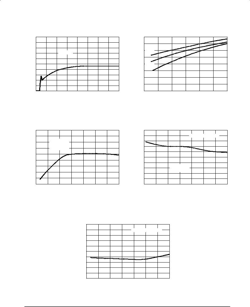
Figure 2. Normalized Output Voltage |
Figure 3. Line Regulation |
|
1.0 |
|
|
|
|
|
|
|
(%) |
0.8 |
Vin = 20 V |
|
|
|
|
|
|
CHANGE |
0.6 |
ILoad = 500 mA |
|
|
|
|
|
|
Normalized at TJ = 25°C |
|
|
|
|
||||
0.4 |
|
|
|
|
||||
|
|
|
|
|
|
|
||
VOLTAGE |
0.2 |
|
|
|
|
|
|
|
0 |
|
|
|
|
|
|
|
|
±0.2 |
|
|
|
|
|
|
|
|
, OUTPUT |
|
|
|
|
|
|
|
|
±0.4 |
|
|
|
|
|
|
|
|
±0.6 |
|
|
|
|
|
|
|
|
out |
±0.8 |
|
|
|
|
|
|
|
V |
|
|
|
|
|
|
|
|
|
±1.0 |
±25 |
0 |
25 |
50 |
75 |
100 |
125 |
|
±50 |
|||||||
|
|
|
TJ, JUNCTION TEMPERATURE (°C) |
|
|
|||
|
1.4 |
|
|
|
|
|
|
|
|
(%) |
1.2 |
ILoad = 500 mA |
|
|
|
|
|
|
|
CHANGE |
|
|
|
|
|
|
|
||
1.0 |
TJ = 25°C |
|
|
|
|
|
|
|
|
0.8 |
|
|
|
|
|
|
|
|
|
|
|
3.3 V, 5.0 V and ADJ |
|
|
|
|
|||
VOLTAGE |
0.6 |
|
|
|
|
|
|||
0.4 |
|
|
|
|
|
|
|
|
|
0.2 |
|
|
|
|
|
|
|
|
|
OUTPUT |
|
|
|
|
|
12 V and 15 V |
|
|
|
0 |
|
|
|
|
|
|
|
||
|
|
|
|
|
|
|
|
||
±0.2 |
|
|
|
|
|
|
|
|
|
, |
|
|
|
|
|
|
|
|
|
|
|
|
|
|
|
|
|
|
|
out |
±0.4 |
|
|
|
|
|
|
|
|
V |
|
|
|
|
|
|
|
|
|
|
|
|
|
|
|
|
|
|
|
|
±0.6 |
5.0 |
10 |
15 |
20 |
25 |
30 |
35 |
40 |
|
0 |
||||||||
|
|
|
|
Vin, INPUT VOLTAGE (V) |
|
|
|||
Figure 4. Dropout Voltage |
Figure 5. Current Limit |
|
2.0 |
|
|
|
|
|
|
|
(V) |
|
ILoad = 3.0 A |
|
|
|
|
||
DIFFERENTIAL |
|
|
|
|
|
|||
1.5 |
|
|
|
|
|
|
|
|
1.0 |
|
|
|
|
|
|
|
|
± OUTPUT |
|
|
|
|
|
|
|
|
|
|
|
ILoad = 500 mA |
|
|
|
|
|
0.5 |
|
|
|
|
|
|
|
|
INPUT |
|
|
|
|
|
|
|
|
|
|
|
|
|
|
L1 = 150 μH |
||
|
|
|
|
|
|
Rind = 0.1 |
Ω |
|
|
|
|
|
|
|
|
||
|
0 |
±25 |
0 |
25 |
50 |
75 |
100 |
125 |
|
±50 |
|||||||
|
|
|
TJ, JUNCTION TEMPERATURE (°C) |
|
||||
|
6.5 |
|
|
|
|
|
|
|
(A) |
6.0 |
|
|
|
|
|
Vin = 25 V |
|
|
|
|
|
|
|
|
||
CURRENT |
5.5 |
|
|
|
|
|
|
|
|
|
|
|
|
|
|
|
|
, OUTPUT |
5.0 |
|
|
|
|
|
|
|
|
|
|
|
|
|
|
|
|
O |
4.5 |
|
|
|
|
|
|
|
I |
|
|
|
|
|
|
|
|
|
|
|
|
|
|
|
|
|
|
4.0 |
|
|
|
|
|
|
|
|
±50 |
±25 |
0 |
25 |
50 |
75 |
100 |
125 |
|
|
|
TJ, JUNCTION TEMPERATURE (°C) |
|
|
|||
Figure 6. Quiescent Current |
Figure 7. Standby Quiescent Current |
|
20 |
|
|
|
|
|
|
|
A) |
|
|
|
|
|
|
|
Vout = 5.0 V |
(μ |
|
QUIESCENTCURRENT (mA) |
18 |
|
|
|
|
|
QUIESCENT CURRENT |
||
|
|
|
|
|
|
Measured at |
|||
16 |
|
|
|
|
|
Ground Pin |
|||
14 |
|
|
|
|
|
TJ = 25°C |
|
||
|
|
|
|
|
|
|
|||
12 |
|
|
|
ILoad = 3.0 A |
|
|
|||
|
|
|
|
|
|
|
|||
10 |
|
|
|
|
|
|
|
||
8.0 |
|
ILoad = 200 mA |
|
|
|
|
|||
, |
|
|
|
|
|
|
|
|
STANDBY, |
Q |
|
|
|
|
|
|
|
|
|
I |
6.0 |
|
|
|
|
|
|
|
|
|
4.0 |
|
|
|
|
|
|
|
stby |
|
5.0 |
10 |
15 |
20 |
25 |
30 |
35 |
I |
|
|
0 |
40 |
|||||||
|
|
|
|
Vin, INPUT VOLTAGE (V) |
|
|
|
||
200 |
|
|
|
|
|
|
|
180 |
VON/OFF = 5.0 V |
|
|
|
|
|
|
160 |
|
|
|
|
|
|
|
140 |
|
|
|
|
|
|
|
120 |
|
Vin = 40 V |
|
|
|
|
|
100 |
|
|
|
|
|
|
|
80 |
|
|
|
|
|
|
|
60 |
|
Vin = 12 V |
|
|
|
|
|
40 |
|
|
|
|
|
|
|
20 |
|
|
|
|
|
|
|
0 |
|
|
|
|
|
|
|
±50 |
±25 |
0 |
25 |
50 |
75 |
100 |
125 |
|
|
TJ, JUNCTION TEMPERATURE (°C) |
|
|
|||
MOTOROLA ANALOG IC DEVICE DATA |
5 |
|
LM2576
TYPICAL PERFORMANCE CHARACTERISTICS (Circuit of Figure 15)
Figure 8. Standby Quiescent Current
A) |
200 |
|
|
|
|
|
|
|
|
(μ |
180 |
|
|
|
|
|
|
|
|
CURRENT |
|
|
|
|
|
|
|
|
|
160 |
|
|
|
|
|
|
|
|
|
140 |
|
|
TJ = 25°C |
|
|
|
|
|
|
QUIESCENT |
120 |
|
|
|
|
|
|
|
|
100 |
|
|
|
|
|
|
|
|
|
80 |
|
|
|
|
|
|
|
|
|
, STANDBY |
60 |
|
|
|
|
|
|
|
|
40 |
|
|
|
|
|
|
|
|
|
20 |
|
|
|
|
|
|
|
|
|
stby |
|
|
|
|
|
|
|
|
|
0 |
|
|
|
|
|
|
|
|
|
I |
5 |
10 |
15 |
20 |
25 |
30 |
35 |
40 |
|
|
0 |
||||||||
|
|
|
|
Vin, INPUT VOLTAGE (V) |
|
|
|
||
Figure 10. Oscillator Frequency
|
8.0 |
|
|
|
|
|
|
|
(%) |
6.0 |
|
|
|
|
|
|
|
4.0 |
Vin = 12 V |
|
|
|
|
|
||
FREQUENCY |
|
|
|
|
|
|||
|
Normalized at |
|
|
|
|
|
||
2.0 |
25°C |
|
|
|
|
|
||
0 |
|
|
|
|
|
|
|
|
|
|
|
|
|
|
|
|
|
NORMALIZED |
±2.0 |
|
|
|
|
|
|
|
±4.0 |
|
|
|
|
|
|
|
|
±6.0 |
|
|
|
|
|
|
|
|
±8.0 |
|
|
|
|
|
|
|
|
|
|
|
|
|
|
|
|
|
|
±10 |
±25 |
0 |
25 |
50 |
75 |
100 |
125 |
|
±50 |
|||||||
|
|
|
TJ, JUNCTION TEMPERATURE (°C) |
|
|
|||
Figure 9. Switch Saturation Voltage
|
1.6 |
|
|
|
|
|
|
(V) |
1.4 |
|
|
|
|
|
|
VOLTAGE |
1.2 |
±40°C |
|
|
|
|
|
1.0 |
|
|
|
|
|
|
|
, SATURATION |
0.8 |
25°C |
|
|
|
|
|
0.6 |
125°C |
|
|
|
|
|
|
|
|
|
|
|
|
||
0.4 |
|
|
|
|
|
|
|
sat |
|
|
|
|
|
|
|
|
|
|
|
|
|
|
|
V |
0.2 |
|
|
|
|
|
|
|
|
|
|
|
|
|
|
|
0 |
|
|
|
|
2.5 |
|
|
0 |
0.5 |
1.0 |
1.5 |
2.0 |
3.0 |
SWITCH CURRENT (A)
Figure 11. Minimum Operating Voltage
|
5.0 |
|
|
|
|
|
|
|
|
4.5 |
|
|
|
Adjustable Version Only |
|
||
(V) |
4.0 |
|
|
|
|
|
|
|
3.5 |
|
|
|
|
|
|
|
|
VOLTAGE |
|
|
|
|
|
|
|
|
3.0 |
|
|
|
|
|
|
|
|
2.5 |
|
|
|
|
|
|
|
|
, INPUT |
|
|
|
|
|
|
|
|
2.0 |
|
|
|
|
|
|
|
|
1.5 |
|
|
Vout ' 1.23 V |
|
|
|
|
|
in |
|
|
|
ILoad = 500 mA |
|
|
|
|
V |
1.0 |
|
|
|
|
|
|
|
|
|
|
|
|
|
|
|
|
|
0.5 |
|
|
|
|
|
|
|
|
0 |
±25 |
0 |
25 |
50 |
75 |
100 |
125 |
|
±50 |
|||||||
|
|
|
TJ, JUNCTION TEMPERATURE (°C) |
|
|
|||
Figure 12. Feedback Pin Current
|
100 |
|
|
|
|
|
|
|
(nA) |
80 |
|
|
|
Adjustable Version Only |
|
||
60 |
|
|
|
|
|
|
|
|
CURRENT |
|
|
|
|
|
|
|
|
40 |
|
|
|
|
|
|
|
|
20 |
|
|
|
|
|
|
|
|
PIN |
0 |
|
|
|
|
|
|
|
,FEEDBACK |
±20 |
|
|
|
|
|
|
|
±40 |
|
|
|
|
|
|
|
|
±60 |
|
|
|
|
|
|
|
|
b |
|
|
|
|
|
|
|
|
I |
±80 |
|
|
|
|
|
|
|
|
|
|
|
|
|
|
|
|
|
±100 |
±25 |
0 |
25 |
50 |
75 |
100 |
125 |
|
±50 |
|||||||
|
|
|
TJ, JUNCTION TEMPERATURE (°C) |
|
|
|||
6 |
MOTOROLA ANALOG IC DEVICE DATA |
LM2576
TYPICAL PERFORMANCE CHARACTERISTICS (Circuit of Figure 15)
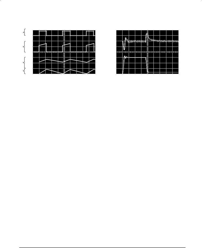
Figure 13. Switching Waveforms
A |
50 V |
|
|
|
0 |
|
4.0 A |
B |
2.0 A |
|
0 |
|
4.0 A |
C |
2.0 A |
|
|
D |
0 |
|
|
|
5 μs/DIV |
Vout = 15 V
A:Output Pin Voltage, 10 V/DIV
B:Inductor Current, 2.0 A/DIV
C:Inductor Current, 2.0 A/DIV, AC±Coupled
D:Output Ripple Voltage, 50mV/dDIV, AC±Coupled
Horizontal Time Base: 5 μs/DIV
Figure 14. Load Transient Response
100 mV |
|
Output |
0 |
Voltage |
|
Change |
|
± 100 mV |
|
|
3.0 A |
Load |
2.0 A |
Current |
|
|
1.0 A |
|
0 |
|
100 μs/DIV |
MOTOROLA ANALOG IC DEVICE DATA |
7 |
|
LM2576
Figure 15. Typical Test Circuit
Fixed Output Voltage Versions
|
|
|
|
|
Feedback |
|
|
|
|
|
|
|
Vin |
LM2576 |
4 |
|
|
|
|
|
|
|
|
|
L1 |
|
|
|
|
|||
|
|
1 |
Fixed Output |
Output |
100 μH |
|
|
|
Vout |
|
|
|
|
|
|
|
|
|
|
||
|
|
|
|
|
2 |
|
|
|
|
|
|
|
3 |
Gnd |
5 |
ON/OFF |
|
|
|
|
|
7.0 V ± 40 V |
Cin |
μF |
|
|
|
D1 |
C |
μ |
|
|
Unregulated |
100 |
|
|
|
out |
F |
|
|||
DC Input |
|
|
|
|
|
MBR360 |
1000 |
|
Load |
|
|
|
|
|
|
|
|
|
|||
|
|
|
|
|
|
|
|
|
|
|
Cin |
± |
100 μF, 75 V, Aluminium Electrolytic |
Cout ± |
1000 μF, 25 V, Aluminium Electrolytic |
|
D1 |
± |
Schottky, MBR360 |
L1 |
± |
100 μH, Pulse Eng. PE±92108 |
R1 |
± |
2.0 k, 0.1% |
R2 |
± |
6.12 k, 0.1% |
Adjustable Output Voltage Versions
|
|
|
|
|
Feedback |
|
|
|
|
|
|
|
|
|
Vin |
LM2576 |
4 |
|
|
|
|
|
|
|
|
|
|
|
|
|
L1 |
|
|
Vout |
||||
|
|
1 |
Adjustable |
|
100 μH |
|
|
|||||
|
|
|
|
|
Output |
|
|
|
|
|
5,000 V |
|
|
|
|
|
|
2 |
|
|
|
|
|
|
|
7.0 V ± 40 V |
|
3 |
Gnd |
5 |
ON/OFF |
|
|
|
|
|
|
|
Cin |
|
|
|
|
|
|
|
Cout |
|
|
R2 |
|
Unregulated |
μF |
|
|
|
|
D1 |
μ |
|
||||
100 |
|
|
|
|
F |
|
||||||
DC Input |
|
|
|
|
|
|
|
|
1000 |
|
Load |
|
|
|
|
|
|
|
MBR360 |
|
|
||||
|
|
|
|
|
|
|
|
|
|
|||
|
|
|
|
|
|
|
|
|
|
|
|
R1 |
|
|
|
|
|
Vout + Vref 1.0 ) |
R2 |
|
|
|
|
||
|
|
|
|
|
R1 |
|
|
|
|
|||
|
|
|
|
|
|
|
|
|
|
|
|
|
|
|
|
|
|
R2 + R1 |
Vout |
± 1.0 |
|
|
|
||
|
|
|
|
|
Vref |
|
|
|
||||
|
|
|
|
|
|
|
|
|
|
|
|
|
|
|
|
|
|
Where Vref = 1.23 V, R1 |
|
|
|
|
|||
|
|
|
|
|
between 1.0 k and 5.0 k |
|
|
|
|
|||
PCB LAYOUT GUIDELINES
As in any switching regulator, the layout of the printed circuit board is very important. Rapidly switching currents associated with wiring inductance, stray capacitance and parasitic inductance of the printed circuit board traces can generate voltage transients which can generate electromagnetic interferences (EMI) and affect the desired operation. As indicated in the Figure 15, to minimize inductance and ground loops, the length of the leads indicated by heavy lines should be kept as short as possible.
For best results, single±point grounding (as indicated) or ground plane construction should be used.
On the other hand, the PCB area connected to the Pin 2 (emitter of the internal switch) of the LM2576 should be kept to a minimum in order to minimize coupling to sensitive circuitry.
Another sensitive part of the circuit is the feedback. It is important to keep the sensitive feedback wiring short. To assure this, physically locate the programming resistors near to the regulator, when using the adjustable version of the LM2576 regulator.
8 |
MOTOROLA ANALOG IC DEVICE DATA |
|
|
|
|
LM2576 |
|
|
|
|
PIN FUNCTION DESCRIPTION |
|
|
|
|
|
Pin |
|
|
Symbol |
Description (Refer to Figure 1) |
|
|
|
|
|
1 |
Vin |
This pin is the positive input supply for the LM2576 step±down switching regulator. In order to minimize |
||
|
|
|
|
voltage transients and to supply the switching currents needed by the regulator, a suitable input bypass |
|
|
|
|
capacitor must be present (Cin in Figure 1). |
2 |
Output |
This is the emitter of the internal switch. The saturation voltage Vsat of this output switch is typically 1.5 V. |
||
|
|
|
|
It should be kept in mind that the PCB area connected to this pin should be kept to a minimum in order to |
|
|
|
|
minimize coupling to sensitive circuitry. |
|
|
|
|
|
3 |
Gnd |
Circuit ground pin. See the information about the printed circuit board layout. |
||
|
|
|
|
|
4 |
Feedback |
This pin senses regulated output voltage to complete the feedback loop. The signal is divided by the |
||
|
|
|
|
internal resistor divider network R2, R1 and applied to the non±inverting input of the internal error amplifier. |
|
|
|
|
In the Adjustable version of the LM2576 switching regulator this pin is the direct input of the error amplifier |
|
|
|
|
and the resistor network R2, R1 is connected externally to allow programming of the output voltage. |
|
|
|
|
|
5 |
|
|
|
It allows the switching regulator circuit to be shut down using logic level signals, thus dropping the total |
ON/OFF |
||||
|
|
|
|
input supply current to approximately 80 μA. The threshold voltage is typically 1.4 V. Applying a voltage |
|
|
|
|
above this value (up to +Vin) shuts the regulator off. If the voltage applied to this pin is lower than 1.4 V or |
|
|
|
|
if this pin is left open, the regulator will be in the ªonº condition. |
|
|
|
|
|
|
|
|
|
DESIGN PROCEDURE |
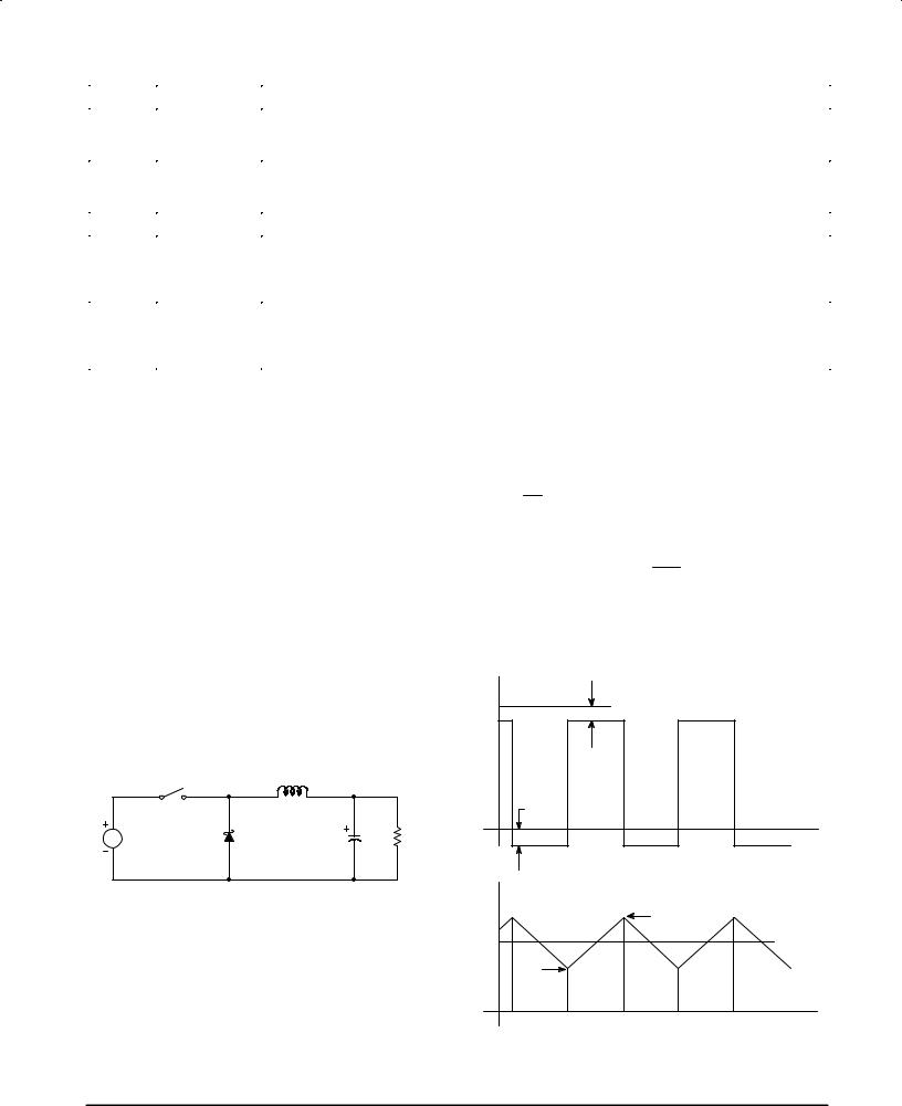
Buck Converter Basics
The LM2576 is a ªBuckº or Step±Down Converter which is the most elementary forward±mode converter. Its basic schematic can be seen in Figure 16.
The operation of this regulator topology has two distinct time periods. The first one occurs when the series switch is on, the input voltage is connected to the input of the inductor.
The output of the inductor is the output voltage, and the rectifier (or catch diode) is reverse biased. During this period, since there is a constant voltage source connected across the inductor, the inductor current begins to linearly ramp upwards, as described by the following equation:
IL(on) + |
Vin ± Vout ton |
|
L |
|
|
During this ªonº period, energy is stored within the core material in the form of magnetic flux. If the inductor is properly designed, there is sufficient energy stored to carry the requirements of the load during the ªoffº period.
|
Figure 16. Basic Buck Converter |
|
|
|
Power |
L |
|
|
Switch |
|
|
|
|
|
|
V |
D |
Cout |
R |
in |
|
|
Load |
The next period is the ªoffº period of the power switch. When the power switch turns off, the voltage across the inductor reverses its polarity and is clamped at one diode voltage drop below ground by the catch diode. The current now flows through the catch diode thus maintaining the load current loop. This removes the stored energy from the inductor. The inductor current during this time is:
IL(off) + |
Vout ± VD toff |
|
L |
|
|
This period ends when the power switch is once again turned on. Regulation of the converter is accomplished by varying the duty cycle of the power switch. It is possible to describe the duty cycle as follows:
d + tonT , where T is the period of switching.
For the buck converter with ideal components, the duty cycle can also be described as:
d + Vout Vin
Figure 17 shows the buck converter, idealized waveforms of the catch diode voltage and the inductor current.
Figure 17. Buck Converter Idealized Waveforms
Von(SW)
Voltage |
Power |
Power |
Power |
Power |
|
Switch |
Switch |
Switch |
Switch |
||
Diode |
|||||
Off |
On |
Off |
On |
||
VD(FWD) |
|
|
|
||
|
|
|
|
||
|
|
|
|
Time |
|
|
|
Ipk |
|
|
Current |
|
|
|
ILoad(AV) |
|
|
|
|
|
||
Inductor |
Imin |
Power |
|
Power |
|
Diode |
Diode |
||||
Switch |
Switch |
||||
|
|
|
|
Time |
MOTOROLA ANALOG IC DEVICE DATA |
9 |
|
 Loading...