


Order this document by LM2935/D
Low Dropout
Dual Voltage Regulator
The LM2935 is a dual positive 5.0 V low dropout voltage regulator, designed for standby power systems. The main output is capable of supplying 750 mA for microprocessor power, and can be turned ªonº and ªoffº by the switch/reset input. The other output is dedicated for standby operation of volatile memory, and is capable of supplying up to 10 mA loads. The total device features a low quiescent current of 3.0 mA or less when supplying 10 mA from the standby output.
This part was designed for harsh automotive environments and is therefore immune to many input supply voltage problems such as reverse battery (±12 V), double battery (+24 V), and load dump transients (+60 V).
•Two Regulated 5.0 V Outputs
•Main Output Current in Excess of 750 mA
•On/Off Control of Main Output
•Standby Output Current in Excess of 10 mA
•Low Input/Output Differential of Less than 0.6 V at 500 mA
•Short Circuit Current Limiting
•Internal Thermal Shutdown
•Low Voltage Indicator Output
•Designed for Automotive Environment Including
•Reverse Battery Protection
•Double Battery Protection
•Load Dump Protection
•Reverse Transient Protection
•Economical 5±Lead TO±220 Package with Two Optional Leadforms
•Also Available in Surface Mount D2PAK Package
ORDERING INFORMATION
|
Operating |
|
|
Device |
Temperature Range |
Package |
|
|
|
|
|
LM2935D2T |
|
Surface Mount |
|
|
|
|
|
LM2935T |
TJ = ±40° to +125°C |
Plastic Power |
|
|
|
||
LM2935TH |
Horizontal Mount |
||
|
|||
|
|
|
|
LM2935TV |
|
Vertical Mount |
|
|
|
|
LM2935
LOW DROPOUT
DUAL VOLTAGE REGULATOR
SEMICONDUCTOR
TECHNICAL DATA
TH SUFFIX
PLASTIC PACKAGE
CASE 314A
|
1 |
|
5 |
|
TV SUFFIX |
1 |
PLASTIC PACKAGE |
|
CASE 314B |
|
5 |
Heatsink surface connected to Pin 3.
T SUFFIX
PLASTIC PACKAGE
CASE 314D
1 

5
Pin 1. Input Voltage/VCC
2.Main Output
3.Ground
4.Switch/Reset
5.Standby/Output
|
D2T SUFFIX |
|
PLASTIC PACKAGE |
|
CASE 936A |
1 |
(D2PAK) |
|
|
|
5 |
Heatsink surface (shown as terminal 6
in case outline drawing) is connected to Pin 3.
Motorola, Inc. 1996 |
Rev 1 |
LM2935
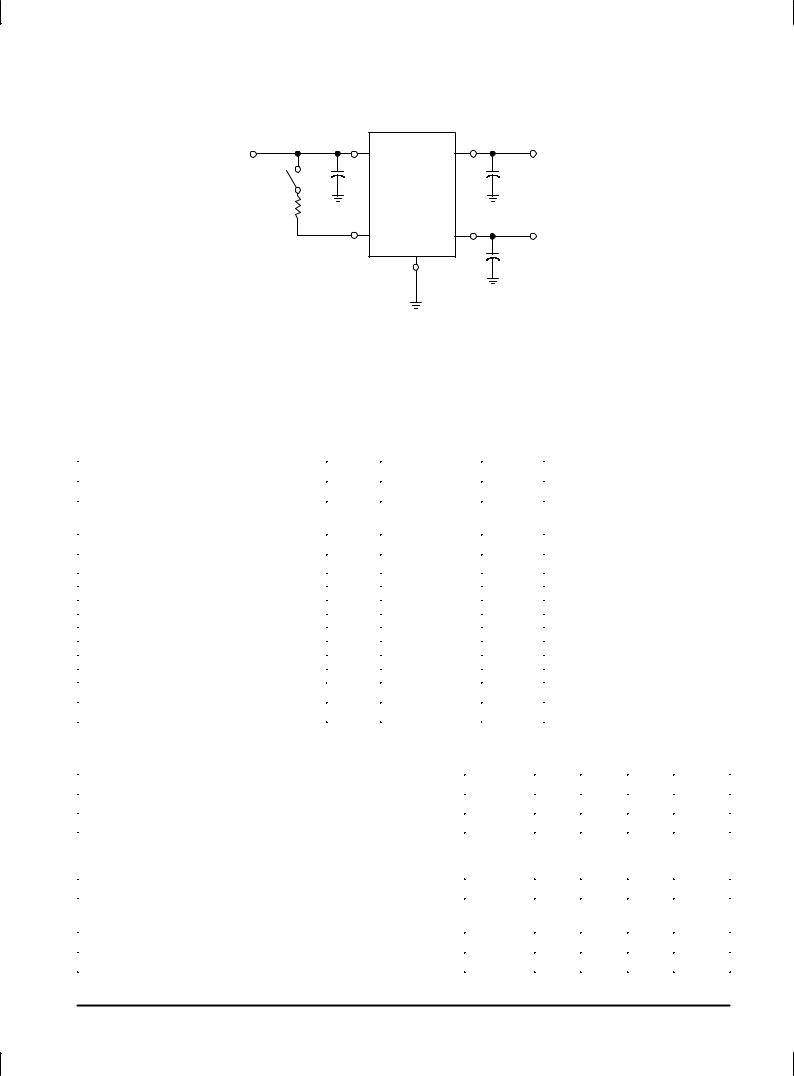
Typical Application Circuit
|
|
|
Main |
|
Input |
|
Output |
Vin |
|
|
|
1 |
2 |
5.0 V/750 mA |
|
|
0.1 |
|
+ |
S1* |
|
10 |
|
|
|
|
|
*The main output |
|
LM2935 |
|
20 k |
|
|
|
is ªOffº with switch |
|
|
|
S1 open. |
|
|
Standby |
|
4 |
5 |
5.0 V/10 mA |
|
Switch/ |
3 |
+ |
|
Reset |
Gnd |
10 |
|
|
|
An input bypass capacitor is recommended if the regulator is located more than 4″ from the supply input filter. The LM2935 is not internally compensated and thus requires an external output capacitor for stability. A minimum capacitance of 10 mF is recommended. The actual capacitance value is dependent upon load current, temperature, and the capacitor's equivalent series resistance (ESR). The least stable condition is encountered at maximum load current and minimum ambient temperature.
This device contains 29 active transistors.
MAXIMUM RATINGS
Rating |
Symbol |
Value |
Unit |
|
|
|
|
Input Voltage Continuous |
VI |
60 |
Vdc |
Transient Reverse Polarity Input Voltage |
±VI(t) |
± 50 |
Vpk |
1.0% Duty Cycle, t ≤ 100 ms |
|
|
|
|
|
|
|
Switch/Reset Input Current |
Iin |
5.0 |
mA |
Power Dissipation |
|
|
|
Case 314A, 314B and 314D (TO±220 Type) |
|
|
|
TA = 25°C |
PD |
Internally Limited |
W |
Thermal Resistance, Junction±to±Ambient |
RqJA |
65 |
°C/W |
Thermal Resistance, Junction±to±Case |
RqJC |
5.0 |
°C/W |
Case 936A (D2PAK) |
|
|
|
TA = 25°C |
PD |
Internally Limited |
W |
Thermal Resistance, Junction±to±Ambient |
RqJA |
Per Figure 1 |
°C/W |
Thermal Resistance, Junction±to±Case |
RqJC |
5.0 |
°C/W |
Operating Junction Temperature Range |
TJ |
± 40 to +150 |
°C |
Storage Temperature Range |
Tstg |
± 65 to +150 |
°C |
ELECTRICAL CHARACTERISTICS (Vin = 14 V, IO = 500 mA, Istby = 0 mA, CO = 10 mF, Cstby = 10 mF, TJ = 25°C [Note 1].)
Characteristic |
Symbol |
Min |
Typ |
Max |
Unit |
|
|
|
|
|
|
MAIN OUTPUT |
|
|
|
|
|
|
|
|
|
|
|
Output Voltage (Vin = 6.0 V to 26 V, IO = 5.0 mA to 500 mA, TJ = ± 40 to +125°C) |
VO |
4.75 |
5.0 |
5.25 |
V |
Line Regulation |
Regline |
|
|
|
mV |
Vin = 9.0 V to 16 V, IO = 5.0 mA |
|
± |
4.0 |
25 |
|
Vin = 6.0 V to 26 V, IO = 5.0 mA |
|
± |
10 |
50 |
|
Load Regulation (IO = 5.0 mA to 500 mA) |
Regload |
± |
10 |
50 |
mV |
Output Impedance |
ZO |
|
|
|
mW |
IO = 500 mAdc and 10 mArms, f = 100 Hz to 10 kHz |
|
± |
200 |
± |
|
Output Noise Voltage (f = 10 Hz to 100 kHz) |
Vn |
± |
100 |
± |
mVrms |
Long Term Stability |
S |
± |
20 |
± |
mV/kHR |
|
|
|
|
|
|
2 |
MOTOROLA ANALOG IC DEVICE DATA |

LM2935
ELECTRICAL CHARACTERISTICS (Vin = 14 V, IO = 500 mA, Istby = 0 mA, CO = 10 μF, Cstby = 10 μF, TJ = 25°C [Note 1].)
Characteristic |
Symbol |
Min |
Typ |
Max |
Unit |
|
|
|
|
|
|
MAIN OUTPUT (continued) |
|
|
|
|
|
|
|
|
|
|
|
Ripple Rejection (f = 120 Hz) |
RR |
± |
66 |
± |
dB |
|
|
|
|
|
|
Dropout Voltage |
VI±VO |
|
|
|
V |
IO = 500 mA |
|
± |
0.45 |
0.6 |
|
IO = 750 mA |
|
± |
0.82 |
± |
|
Short Circuit Current Limit |
ISC |
0.75 |
1.2 |
± |
A |
Over±Voltage Shutdown Threshold |
Vth(OV) |
26 |
31 |
± |
V |
SWITCH/RESET |
|
|
|
|
|
|
|
|
|
|
|
Output Sink Current (VOL = 1.2 V) |
ISink |
± |
5.0 |
± |
mA |
Output Voltage (Ron/off = 20 kΩ) |
|
|
|
|
V |
Low State, Vin = 4.0 V |
VOL |
± |
0.9 |
1.2 |
|
High State, Vin = 14 V |
VOH |
4.5 |
5.0 |
6.0 |
|
Output Pull±Up Resistor, ªOnº/ªOffº (Note 2) |
Ron/off |
± |
20 |
30 |
kΩ |
Output Voltage with Reverse Polarity Input (Vin = ±15 V, RL = 10 Ω) |
±VO |
± 0.6 |
0 |
± |
V |
ELECTRICAL CHARACTERISTICS (Vin = 14 V, IO = 0 mA, Istby = 10 mA, CO = 10 μF, Cstby = 10 μF, TJ = 25°C [Note 1].) |
|
||||
Characteristic |
Symbol |
Min |
Typ |
Max |
Unit |
|
|
|
|
|
|
STANDBY OUTPUT |
|
|
|
|
|
|
|
|
|
|
|
Output Voltage (Vin = 6.0 V to 26 V, Istby = 1.0 mA to 10 mA, TJ = ±40 to +125°C) |
VO(stby) |
4.75 |
5.0 |
5.25 |
V |
Tracking Voltage |
VO±VO(stby) |
± 200 |
0 |
200 |
mV |
Line Regulation (Vin = 6.0 V to 26 V) |
Regline |
± |
4.0 |
50 |
mV |
Load Regulation (Istby = 1.0 mA to 10 mA) |
Regload |
± |
10 |
50 |
mV |
Output Impedance |
ZO(stby) |
|
|
|
Ω |
I(stby) = 10 mAdc and 1.0 mArms, f = 100 Hz to 10 kHz |
|
± |
1.0 |
± |
|
Output Noise Voltage (f = 10 Hz to 100 kHz) |
Vn |
± |
300 |
± |
μVrms |
Long Term Stability |
S |
± |
20 |
± |
mV/kHR |
|
|
|
|
|
|
Ripple Rejection (f = 120 Hz) |
RR |
± |
66 |
± |
dB |
|
|
|
|
|
|
Dropout Voltage (Istby = 10 mA) |
VI±VO(stby) |
± |
0.55 |
0.7 |
V |
Short Circuit Current Limit |
ISC |
25 |
70 |
± |
mA |
Output Voltage with Reverse Polarity Input |
±VO |
|
|
|
V |
Vin = ±15 V, RL = 510 Ω |
|
± 0.3 |
0 |
± |
|
Output Voltage with Maximum Positive Input |
VO(max) |
|
|
|
V |
Vin = 60 V, RL = 510 Ω |
|
± |
5.0 |
6.0 |
|
TOTAL DEVICE |
|
|
|
|
|
|
|
|
|
|
|
Bias Current |
IB |
|
|
|
mA |
IO = 10 mA, Istby = 0 mA |
|
± |
3.0 |
± |
|
IO = 500 mA, Istby = 0 mA |
|
± |
40 |
100 |
|
IO = 750 mA, Istby = 0 mA |
|
± |
90 |
± |
|
Main Output ªOffº, I = 10 mA |
|
± |
2.0 |
3.0 |
|
stby |
|
|
|
|
|
NOTES: 1. Low duty cycle pulse techniques are used during test to maintain junction temperature as close to ambient as possible. 2. The maximum switch/reset current must not exceed 5.0 mA.
MOTOROLA ANALOG IC DEVICE DATA |
3 |
|
 Loading...