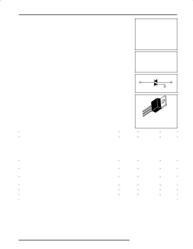
Motorola MAC228-6, MAC228-4, MAC228-10, MAC228A8, MAC228A4 Datasheet
...
MOTOROLA
SEMICONDUCTOR TECHNICAL DATA
Order this document by MAC228/D
Triacs
Silicon Bidirectional Triode Thyristors
. . . designed primarily for industrial and consumer applications for full wave control of ac loads such as appliance controls, heater controls, motor controls, and other power switching applications.
•Sensitive Gate Triggering in 3 Modes for AC Triggering on Sinking Current Sources (MAC228 Series)
•Four Mode Triggering for Drive Circuits that Source Current (MAC228A Series)
•All Diffused and Glass-Passivated Junctions for Parameter Uniformity and Stability
•Small, Rugged, Thermowatt Construction for Low Thermal resistance and High Heat Dissipation
•Center Gate Geometry for Uniform Current Spreading
MAXIMUM RATINGS (TJ = 25°C unless otherwise noted.)
MAC228
Series
MAC228A
Series
TRIACs
8 AMPERES RMS
200 thru 800 VOLTS
MT2 |
MT1 |
|
G |
CASE 221A-04 (TO-220AB)
STYLE 4
Rating |
Symbol |
Value |
Unit |
|
|
|
|
Peak Repetitive Off-State Voltage(1) |
VDRM |
|
Volts |
(TJ = ±40 to 110°C |
|
|
|
1/2 Sine Wave 50 to 60 Hz, Gate Open) |
|
|
|
MAC228-4, MAC228A4 |
|
200 |
|
MAC228-6, MAC228A6 |
|
400 |
|
MAC228-8, MAC228A8 |
|
600 |
|
MAC228-10, MAC228A10 |
|
800 |
|
|
|
|
|
On-State RMS Current (TC = 80°C) |
IT(RMS) |
8 |
Amps |
Full Cycle Sine Wave 50 to 60 Hz |
|
|
|
|
|
|
|
Peak Non-repetitive Surge Current |
ITSM |
80 |
Amps |
(One Full Cycle 60 Hz, TJ = 110°C) |
|
|
|
Circuit Fusing |
I2t |
26 |
A2s |
(t = 8.3 ms) |
|
|
|
|
|
|
|
Peak Gate Current (t p 2 μs) |
IGM |
±2 |
Amps |
Peak Gate Voltage (t p 2 μs) |
VGM |
±10 |
Volts |
Peak Gate Power (t p 2 μs) |
PGM |
20 |
Watts |
1. VDRM for all types can be applied on a continuous basis. Blocking voltages shall not be tested with a constant current |
(continued) |
||
source such that the voltage ratings of the devices are exceeded. |
|
|
|
Motorola, Inc. 1995

MAC228 Series MAC228A Series
MAXIMUM RATINGS Ð continued
Rating |
Symbol |
Value |
Unit |
|
|
|
|
Average Gate Power (TC = 80°C, t p 8.3 ms) |
PG(AV) |
0.5 |
Watts |
Operating Junction Temperature Range |
TJ |
±40 to 110 |
°C |
Storage Temperature Range |
Tstg |
±40 to 150 |
°C |
Mounting Torque |
|
8 |
in. lb. |
|
|
|
|
THERMAL CHARACTERISTICS |
|
|
|
|
Characteristic |
|
|
Symbol |
|
Max |
|
|
Unit |
||
|
|
|
|
|
|
|
|
|
|
|
|
Thermal Resistance, Junction to Case |
|
|
RθJC |
2.2 |
|
|
°C/W |
||||
Thermal Resistance, Junction to Ambient |
|
|
RθJA |
60 |
|
|
°C/W |
||||
ELECTRICAL CHARACTERISTICS (TC = 25°C and either polarity of MT2 to MT1 voltage unless otherwise noted.) |
|
|
|
|
|||||||
|
Characteristic |
Symbol |
|
Min |
|
Typ |
Max |
|
Unit |
||
|
|
|
|
|
|
|
|
|
|
|
|
Peak Blocking Current |
TJ = 25°C |
IDRM |
|
Ð |
|
Ð |
10 |
|
μA |
||
(VD = Rated VDRM) |
|
|
|
|
|
||||||
|
TJ = 110°C |
|
|
|
Ð |
|
Ð |
2 |
|
mA |
|
Peak On-State Voltage |
|
VTM |
|
Ð |
|
Ð |
1.8 |
|
Volts |
||
(ITM = 11 A Peak, Pulse Width p 2 ms, Duty Cycle p 2%) |
|
|
|
|
|
|
|
|
|
|
|
Gate Trigger Current (Continuous dc) |
IGT |
|
|
|
|
|
|
|
mA |
||
(VD = 12 V, RL = 100 Ω) |
|
|
|
|
|
|
|
|
|
|
|
MT2(+), G(+); MT2(+), G(±); MT2(±), G(±) |
|
|
|
Ð |
|
Ð |
5 |
|
|
||
MT2(±), G(+) ªAº Suffix Only |
|
|
|
Ð |
|
Ð |
10 |
|
|
||
|
|
|
|
|
|
|
|
|
|
||
Gate Trigger Voltage (Continuous dc) |
VGT |
|
|
|
|
|
|
|
Volts |
||
(VD = 12 V, RL = 100 Ω) |
|
|
|
|
|
|
|
|
|
|
|
MT2(+), G(+); MT2(+), G(±); MT2(±), G(±) |
|
|
|
Ð |
|
Ð |
2 |
|
|
||
MT2(±), G(+) ªAº Suffix Only |
|
|
|
Ð |
|
Ð |
2.5 |
|
|
||
(VD = Rated VDRM, TC = 110°C, RL = 10 k) |
|
|
|
|
|
|
|
|
|
|
|
MT2(+), G(+); MT2(+), G(±); MT2(±), G(±) |
|
|
|
0.2 |
|
Ð |
Ð |
|
|
||
MT2(±), G(+) ªAº Suffix Only |
|
|
|
0.2 |
|
Ð |
Ð |
|
|
||
|
|
|
|
|
|
|
|
|
|
||
Holding Current |
|
IH |
|
Ð |
|
Ð |
15 |
|
mA |
||
(VD = 12 Vdc, ITM = 200 mA, Gate Open) |
|
|
|
|
|
|
|
|
|
|
|
Gate-Controlled Turn-On Time |
tgt |
|
Ð |
|
1.5 |
Ð |
|
μs |
|||
(VD = Rated VDRM, ITM = 16 A Peak, IG = 30 mA) |
|
|
|
|
|
|
|
|
|
|
|
Critical Rate of Rise of Off-State Voltage |
dv/dt |
|
Ð |
|
25 |
Ð |
|
V/μs |
|||
(VD = Rated VDRM, Exponential Waveform, TC = 110°C) |
|
|
|
|
|
|
|
|
|
|
|
Critical Rate of Rise of Commutation Voltage |
dv/dt(c) |
|
Ð |
|
5 |
Ð |
|
V/μs |
|||
(VD = Rated VDRM, ITM = 11.3 A, |
|
|
|
|
|
|
|
|
|
|
|
Commutating di/dt = 4.1 A/ms, Gate Unenergized, TC = 80°C) |
|
|
|
|
|
|
|
|
|
|
|
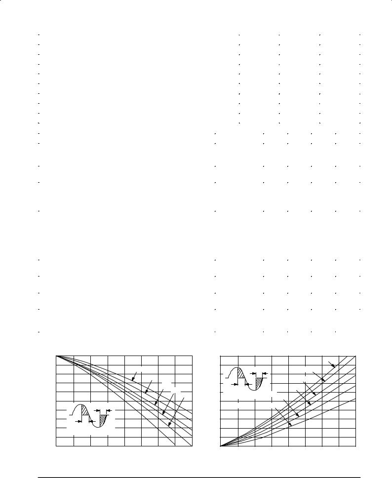
FIGURE 1 ± RMS CURRENT DERATING
|
110 |
|
|
|
|
|
|
|
|
°C) |
104 |
|
|
|
|
α = 30° |
|
|
|
|
|
|
|
|
60° |
|
|
||
( |
|
|
|
|
|
|
|
||
TEMPERATURE |
|
|
|
|
|
|
|
|
|
|
|
|
|
|
|
90° |
120° |
|
|
98 |
|
|
|
|
|
|
180° |
||
|
|
|
|
|
|
|
|||
|
|
|
|
|
|
|
|
||
92 |
|
|
α |
|
|
|
|
|
|
CASE |
|
|
|
|
|
|
|
||
|
|
α |
|
|
|
|
|
|
|
, |
|
|
|
|
|
|
|
|
|
C |
86 |
|
|
|
|
|
|
|
|
T |
α = CONDUCTION ANGLE |
|
|
dc |
|
|
|||
|
|
|
|
|
|
||||
|
80 |
|
2.0 |
3.0 |
4.0 |
|
6.0 |
7.0 |
8.0 |
|
0 |
1.0 |
5.0 |
||||||
|
|
|
IT(RMS), RMS ON-STATE CURRENT (AMP) |
|
|
||||
FIGURE 2 ± ON-STATE POWER DISSIPATION
|
10 |
|
|
|
|
|
dc |
|
|
|
|
|
|
|
|
|
|
|
|
(WATTS) |
8.0 |
|
α |
|
|
α = 180° |
|
|
|
|
|
|
120° |
|
|
|
|||
|
α |
|
|
|
|
|
|
||
|
|
|
|
|
|
|
|
||
POWER |
|
|
|
|
90° |
|
|
|
|
6.0 |
α = CONDUCTION ANGLE 60° |
|
|
|
|||||
|
|
|
|
||||||
|
|
|
|
|
|||||
|
|
|
|
|
|
|
|
|
|
, AVERAGE |
4.0 |
TJ ≈ 110°C |
|
30° |
|
|
|
|
|
|
|
|
|
|
|
|
|
||
|
|
|
|
|
|
|
|
|
|
(AV) |
2.0 |
|
|
|
|
|
|
|
|
|
|
|
|
|
|
|
|
|
|
P |
|
|
|
|
|
|
|
|
|
|
0 |
|
|
|
|
|
|
|
|
|
0 |
1.0 |
2.0 |
3.0 |
4.0 |
5.0 |
6.0 |
7.0 |
8.0 |
|
|
IT(RMS), RMS ON-STATE CURRENT (AMP) |
|
|
|||||
2 |
Motorola Thyristor Device Data |
 Loading...