


LM393
现货库存、技术资料、百科信息、热点资讯,精彩尽在鼎好!
Order this document by LM393/D
The LM393 series are dual independent precision voltage comparators
capable of single or split supply operation. These devices are designed to
permit a common mode range–to–ground level with single supply operation.
Input offset voltage specifications as low as 2.0 mV make this device an
excellent selection for many applications in consumer automotive, and
industrial electronics.
• Wide Single–Supply Range: 2.0 Vdc to 36 Vdc
• Split–Supply Range: ±1.0 Vdc to ±18 Vdc
• Very Low Current Drain Independent of Supply Voltage: 0.4 mA
• Low Input Bias Current: 25 nA
• Low Input Offset Current: 5.0 nA
• Low Input Offset V oltage: 2.0 mV (max) LM393A
5.0 mV (max) LM293/393
• Input Common Mode Range to Ground Level
• Differential Input V oltage Range Equal to Power Supply Voltage
• Output Voltage Compatible with DTL, ECL, TTL, MOS, and CMOS Logic
Levels
• ESD Clamps on the Inputs Increase the Ruggedness of the Device
without Affecting Performance
SINGLE SUPPLY, LOW POWER
DUAL COMPARATORS
SEMICONDUCTOR
TECHNICAL DATA
8
1
N SUFFIX
PLASTIC PACKAGE
CASE 626
8
1
D SUFFIX
PLASTIC PACKAGE
CASE 751
(SO–8)
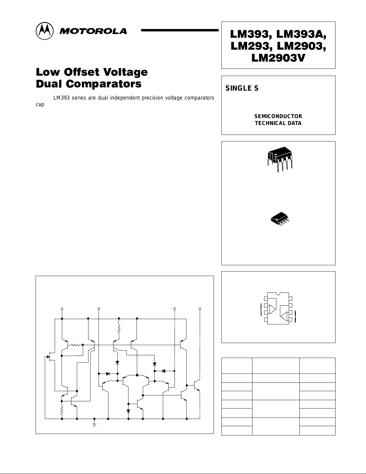
Representative Schematic Diagram
(Diagram shown is for 1 comparator)
F1
R1
4.6 k
V
CC
R4
Q3
2.0 k
Q1
+ Input – Input Output
R2
2.1 k
Q4
Q5
Q8
Q2
Q9
MOTOROLA ANALOG IC DEVICE DATA
Q6
Q10
Q11
Q12
Q15
Q14
Q16
PIN CONNECTIONS
–
+
8
V
CC
7
Output B
6
5
Inputs B
Output A
Inputs A
Gnd
1
2
–
+
3
4
(Top View)
ORDERING INFORMATION
Operating
Device
LM293D
LM393D
LM393AN,N
LM2903D
LM2903N
LM2903VD
LM2903VN
Motorola, Inc. 1996 Rev 1
Temperature Range
TA = –25° to +85°C
TA = 0° to +70°C
TA = –40° to +105°C
TA = –40° to +105°C
Package
SO–8
SO–8
Plastic DIP
SO–8
Plastic DIP
SO–8
Plastic DIP
1
LM393, LM393A, LM293, LM2903, LM2903V
MAXIMUM RATINGS
Rating Symbol Value Unit
Power Supply Voltage V
Input Differential Voltage Range V
Input Common Mode Voltage Range V
Output Short Circuit–to–Ground I
Output Sink Current (Note 1) I
Power Dissipation @ TA = 25°C P
Derate above 25°C 1/R
Operating Ambient Temperature Range T
CC
IDR
ICR
SC
Sink
D
θJA
A
LM293 –25 to +85
LM393, 393A 0 to +70
LM2903 –40 to +105
LM2903V –40 to +125
Maximum Operating Junction Temperature T
J(max)
LM393, 393A, 2903, LM2903V 125
LM293 150
Storage Temperature Range T
stg
+36 or ±18 Vdc
–0.3 to +36 Vdc
Continuous mA
–65 to +150 °C
36 Vdc
20
570 mW
5.7 mW/°C
°C
°C
ELECTRICAL CHARACTERISTICS (V
= 5.0 Vdc, T
CC
≤ TA ≤ T
low
,* unless otherwise noted.)
high
LM393A
Characteristic Symbol
Input Offset Voltage (Note 2) V
IO
Min Typ Max
TA = 25°C – ±1.0 ±2.0
T
≤ TA ≤ T
low
high
Input Offset Current I
IO
– – 4.0
TA = 25°C – ±50 ±50
T
≤ TA ≤ T
low
high
Input Bias Current (Note 3) I
IB
– – ±150
TA = 25°C – 25 250
T
≤ TA ≤ T
low
high
Input Common Mode Voltage Range (Note 4) V
ICR
– – 400
TA = 25°C 0 – VCC –1.5
T
≤ TA ≤ T
low
high
Voltage Gain RL ≥ 15 kΩ, VCC = 15 Vdc, TA = 25°C A
VOL
0 – VCC –2.0
50 200 – V/mV
Large Signal Response Time – – 300 – ns
Vin = TTL Logic Swing, V
= 1.4 Vdc
ref
VRL = 5.0 Vdc, RL = 5.1 kΩ, TA = 25°C
Response Time (Note 5) VRL = 5.0 Vdc, RL = 5.1 kΩ, TA = 25°C t
Input Differential Voltage (Note 6)
All Vin ≥ Gnd or V– Supply (if used)
Output Sink Current
Vin ≥ 1.0 Vdc, V
= 0 Vdc, VO ≤ 1.5 Vdc, TA = 25°C
in+
Output Saturation Voltage V
Vin ≥ 1.0 Vdc, V
T
≤ TA ≤ T
low
*T
= 0°C, T
low
NOTES: 1. The maximum output current may be as high as 20 mA, independent of the magnitude of VCC, output short circuits to VCC can cause excessive
high
heating and eventual destruction.
2.At output switch point, VO]
3.Due to the PNP transistor inputs, bias current will flow out of the inputs. This current is essentially constant, independent of the output state, there
fore, no loading changes will exist on the input lines.
4.Input common mode of either input should not be permitted to go more than 0.3 V negative of ground or minus supply. The upper limit of common
mode range is VCC –1.5 V.
5.Response time is specified with a 100 mV step and 5.0 mV of overdrive. With larger magnitudes of overdrive faster response times are obtainable.
6.The comparator will exhibit proper output state if one of the inputs becomes greater than VCC, the other input must remain within the common mode
range. The low input state must not be less than –0.3 V of ground or minus supply.
= 0 Vdc, I
in+
Sink
high
= +70°C for LM393/393A
1.4 Vdc, RS = 0 Ω with VCC from 5.0 Vdc to 30 Vdc, and over the full input common mode range (0 V to VCC = –1.5 V).
≤ 4.0 mA, TA = 25°C – 150 400
TLH
V
I
Sink
ID
OL
– 1.3 – µs
– – V
CC
6.0 16 – mA
– – 700
Unit
mV
nA
nA
V
V
mV
2
MOTOROLA ANALOG IC DEVICE DATA
 Loading...